EP0097166B1 - Digital loop transceiver for interfacing a digital pabx to a digital subscriber set via a subscriber line - Google Patents
Digital loop transceiver for interfacing a digital pabx to a digital subscriber set via a subscriber line Download PDFInfo
- Publication number
- EP0097166B1 EP0097166B1 EP82903416A EP82903416A EP0097166B1 EP 0097166 B1 EP0097166 B1 EP 0097166B1 EP 82903416 A EP82903416 A EP 82903416A EP 82903416 A EP82903416 A EP 82903416A EP 0097166 B1 EP0097166 B1 EP 0097166B1
- Authority
- EP
- European Patent Office
- Prior art keywords
- digital
- digital data
- signalling bit
- subscriber line
- data words
- Prior art date
- Legal status (The legal status is an assumption and is not a legal conclusion. Google has not performed a legal analysis and makes no representation as to the accuracy of the status listed.)
- Expired
Links
Images


Classifications
-
- H—ELECTRICITY
- H04—ELECTRIC COMMUNICATION TECHNIQUE
- H04Q—SELECTING
- H04Q11/00—Selecting arrangements for multiplex systems
- H04Q11/04—Selecting arrangements for multiplex systems for time-division multiplexing
- H04Q11/0428—Integrated services digital network, i.e. systems for transmission of different types of digitised signals, e.g. speech, data, telecentral, television signals
Definitions
- This invention relates generally to digital telephone systems and, more particularly, to a digital loop transceiver for use in a digital telephone system comprising a digital PABX and a plurality of digital subscriber sets.
- Becker et al. teach in EP-A-0 036 622, U.S. Patent 4,397,030, a digital communication system utilizing eight speech bits, a synchroniza- tion/signalling bit and a data bit in a thirty-two word format.
- the system receives data in frame format comprising thirty-two ten bit words. Each ten bit word has eight data bits, a synchroniza- tion/signalling bit and an additional data bit.
- the system also transmits data in the same frame format.
- the system taught by Becker et al. does not fully utilize the bandwith capacity of the signalling channel for useful data. Additional circuitry is also required in the frame oriented system of Becker et al. to implement a pattern search and recognition algorithm required to obtain data synchronization.
- a digital loop transceiver circuit which provides duplex communication of digital data words on either a single or on first and second channels and a signalling bit associated with at least one of the channels. Communication is between a duplex subscriber line and a digital I/O port.
- the circuit has a receiver for successively receiving a first and a second of the digital data words and the signalling bit in synchronization with a receive data clock.
- the first digital data word and the signalling bit are received from the digital 1/0 port in response to a first channel receive enable signal.
- the second digital data word is received from the digital I/0 port in response to a second channel receive enable signal.
- the circuit also has a transmitter for transmitting third and fourth digital data words and the signalling bit in synchronization with a transmit data clock.
- the third digital data word is transmitted to the digital I/O port in response to a first channel transmit enable signal.
- the fourth digital data word is transmitted to the digital data port in response to a second channel transmit enable signal.
- the circuit is characterized by modulation means for serially modulating the first and second digital data words and the respective signalling bit for transmission via a first portion of the subscriber line, the first and second data words and the respective signalling bit being received from the digital I/O port in response to at least one receive enable signal (RE1); sync detection means for providing a valid sync signal to synchronize the digital loop transceiver circuit in response to detecting the energy of a differential phase shift keyed signal having a predetermined frame length on a second portion of said subscriber line, said modulated signal comprising a third and a fourth digital data word and respective signalling bit; and demodulation means for serially demodulating data in response to said valid sync signal, said demodulation means demodulating the third and fourth digital data words and said signalling bit received via the second portion of the subscriber line.
- modulation means for serially modulating the first and second digital data words and the respective signalling bit for transmission via a first portion of the subscriber line, the first and second data words and the respective signalling
- a conventional private automatic branch exchange (PABX) 10 comprised generally of a main call processor 12 having associated memory 14, a time slot interchange circuit 16, a set of call processing microprocessors 18-18', each having an associated memory 20-20', and a plurality of conventional analog line cards 22.
- the PABX 10 also includes at least two digital line cards 22' constructed in accordance with the present invention.
- the main call processor 12 coordinates, via a system bus 24, the call processing activities of each of the several call processing microprocessors 18-18'.
- each of the call processing microprocessors 18-18' controls, via respective control buses 26-26', the communication of digital PCM voice data words via respective data buses 28-28' between the several line cards 22 assigned to such microprocessor 18-18'.
- each of the analog line cards 22 comprises a time slot assignment and control circuit (TSAC) 30 for selectively enabling a codec/ filter 32 to digitally encode an analog voice input signal received via a subscriber line interface circuit (SLIC) 34 from a conventional single channel subscriber set (not shown) coupled to tip and ring conductors for output as a digital pulse code modulation (PCM) voice data word on the respective data bus 28-28', and to decode a digital PCM voice data word received on the data bus 28-28' for output as an analog voice output signal to the subscriber set (not shown) via the SLIC 34.
- Shown in Figure 2 is a circuit schematic for such a conventional analog line card 22, using components commercially available from Motorola.
- the various control and data signals which are provided to or by the line card 22 are generally referred to as the "backplane" of the PABX 10.
- the TSAC 30 on the source line card 22 initially detects via the associated SLIC 34 that the source subscriber set is off hook, and routes the call routing information to the call processing microprocessor 18 for transfer to the main call processor 12. If the destination line card 22 is not indicated in the memory 14 as being busy, the main call processor 12 then requests the call processing microprocessor 18' to notify the destination line card 22 of the call.
- the call processing microprocessor 18' advises the main call processor 12 that the requested connection has been established.
- the TSAC 30 on the source line card 22 enables the associated codec/filter 32 to encode the analog voice signal then being received from the source subscriber set via the SLIC 34 for output as a digital PCM voice data word onto the data bus 28.
- the main call processor 12 has enabled the time slot interchange circuit 16 to couple the data bus 28 to the data bus 28' to facilitate the requested intra-exchange communication of the digital PCM voice data word.
- the TSAC 30 on the destination line card 22 enables the associated codec/filter 32 to decode the digital PCM voice data word on the data bus 28' for output as an analog voice signal to the destination subscriber set via the SLIC 34.
- the destination line card 22 is allowed to encode the analog voice signal received from the destination subscriber set for transmission as a digital PCM voice data word via data bus 28', interchange circuit 16 and data bus 28' to the source line card 22 for decoding and output to the source subscriber set. If this exchange of digital PCM voice data words occurs at a sufficiently high frame rate, say of the order of 8 kHz, then it will appear to each of the subscribers that there is a direct analog link between their respective subscriber sets.
- each of the digital line cards 22' comprises a time slot assignment and control circuit (TSAC) 30' for selectively enabling a digital loop transceiver (DLT) 36 (see Figure 5) to receive digital data words via a subscriber line interface network 38 from a dual channel, digital subscriber set, such as that shown in Figure 4, which is coupled to respective receive and transmit pairs of tip and ring conductors, for direct output on the respective data bus 28-28' in the same manner as the digital PCM voice data words are output by the codec/filter 32 in the analog line cards 22; and to receive digital data words on the data bus 28-28' for direct output to the subscriber set via the subscriber line interface network 38.
- TSAC time slot assignment and control circuit
- DLT digital loop transceiver
- FIG. 3 Shown in Figure 3 is a circuit schematic for the digital line card 22', wherein: the TSAC 30' comprises a pair of the Motorola time slot assignment circuits (TSACs), one for each of the two digital communication channels the digital line card 22' is capable of simultaneously supporting; the DLT 36 comprises an integrated circuit constructed in accordance with Figure 5; and the subscriber line interface network 38 comprises a transit isolation transformer 40 coupled to the tip and ring conductors which comprise the receive pair of the subscriber line and a receive isolation transformer 42 coupled to the tip and ring conductors which comprise the transmit pair of the subscriber line. As illustrated in Figure 3, the digital line card 22' responds to and provides the same control and data signals which are provided to or by the analog line card 22 via the backplane of the PABX 10.
- TSACs Motorola time slot assignment circuits
- the subscriber set 44 comprises a digital loop transceiver (DLT) 36' (see Figure 5) for receiving digital data words from the digital line card 22' (see Figure 3) via a subscriber line interface network 38' coupled to respective receive and transmit pairs of tip and ring conductors, for output, if digital PCM voice data words, to a conventional codec/filter 32' for subsequent decoding and output as an analog voice output via a voice I/O network 46, or, if digital data words, to a subscriber data processor (not shown) via a data port 48; and for transmitting digital data words provided either by the codec/filter 32' in the form of digital PCM voice data words of by the subscriber data processor in the form of digital data words, to the digital line card 22' via the subscriber line interface network 38'.
- DLT digital loop transceiver
- the voice I/O network 46 includes a voice input portion 50, and a voice output portion 52;
- the DLT 36' comprises an integrated circuit constructed in accordance with Figure 5;
- the subscriber line interface network 38' comprises a transmit isolation transformer 40' coupled to the tip and ring conductors which comprise the transmit pair of the subscriber line and a receive isolation transformer 42' coupled to the tip and ring conductors which comprise the receive pair of the subscriber line.
- a conventional tone generator 54 such as the Mostek MK5087, interacts with a dial keypad 56 and the voice 1/O network 46 to provide the call routing information required to establish each of the two communication channels, while a conventional hook switch 58 provides call initiation signalling intormation to the DLT 36'.
- An audible indication of an incoming call is provided via a ringing transducer 60.
- a subscriber set power supply 62 derives operating power for the several components of the subscriber set 44 from the subscriber line in a conventional manner.
- the DLT 36 comprises a digital interface portion 64 for interfacing with the PABX 10 in a master operating mode and with the codec/filter 32 and subscriber data processor in a slave operating mode, a modulator/demodulator portion 66 for transmitting and receiving digital data words via the subscriber line, and a sequencer and control portion 68 for controlling the sequence of operations performed by the digital interface and modulator/demodulator portions 64 and 66, respectively.
- a receive (RX) control circuit 70 responds to either of two channel receive enable signals, RE1 and RE2, by enabling a receive (RX) register 72 of the shift register type to serially receive digital data bits via a receive (RX) terminal in synchronization with a receive data clock (RDC) on a CLK/RDC terminal.
- RRC receive data clock
- the sequencer and control portion 68 enables the RX register 72 to transfer the "transmit" frame of data in parallel into a transmitter (XMIT) register 74 in the modulator/demodulator portion 66.
- the then-current states of the two channel signalling bits on respective S11 and S21 terminals are latched and inserted into the frame of data in the XMIT register 74.
- the sequencer and control portion 68 enables a transmit (TX) register 76 to receive a "receive" frame of data in parallel from a receiver (RCV) register 78 in the modulator/demodulator portion 66.
- the two channel signalling bits in the receive frame of data are latched and outputted on respective S10 and S20 terminals.
- a transmit (TX) control circuit 80 enables the TX register 76 to serially transmit the receive frame of data via a TX terminal in synchronization with a transmit data clock (TDC) on an X1/TDC terminal.
- TDC transmit data clock
- a digital to analog converter (DAC) control circuit 82 periodically enables a digital to analog converter (DAC) 84 to transmit the transmit frame of data in the XMIT register 74 to the transmit transformer 40 in the subscriber line interface network 38 using a differential pair of output drivers 86 and 88 coupled to respective line output terminals L01 and L02.
- the DAC 84 utilizes a burst differential phase shift keyed (DPSK) modulation technique at a carrier frequency of 265 kHz.
- DPSK differential phase shift keyed
- an input buffer 90 of the differential to single ended output type in the modulation/ demodulation portion 66 couples the signal received from the receive transformer 42 in the subscriber line interface network 38 via line input terminals LI1 and LI2 to a sync detector 92 via a window detector 94 and to a correlator 96 via a comparator 98.
- the correlator 96 As phase shifts of the proper form are decoded by the correlator 96, the "decoded" bits are shifted into a shift register portion thereof which maintains the most recently received set of data bits which might constitute a frame.
- the sync detector 92 When the energy of a DPSK signal of the proper frame length is detected, the sync detector 92 provides a valid sync signal to enable the correlator 96 to transfer the receive frame of data bits being maintained therein, in parallel to the RCV register 78.
- a switched capacitor bandgap reference 100 similar to that shown and described in WO-A-82/02806 provides a precision reference voltage to the DAC 84, the window detector 94, and the comparator 98. Periodically, the offsets of the input buffer 90, the window detector 94, the comparator 98, and the bandgap reference 100 are zeroed by an auto-zero circuit 102 in a manner similar to that shown and described in WO-A-82/02804.
- the DLT 36 provides duplex communication of digital data words on a pair of independent channels and a signalling bit associated with each of the channels, between the duplex subscriber line and a digital data port.
- the RX register 72 successively receives a digital data word for each of the channels in synchronization with the receive data clock, with the digital data word for the first of the channels being received from the digital I/0 port via the RX terminal in response to the first of the channel receive enable signals, RE1, and the digital data word for the second of the channels being received from the digital I/O port via the RX terminal in response to the second of the channel receive enable signals, RE2.
- both data words are transferred to the XMIT register 74, and the then-current states of the respective channel signalling bits on the S11 and S21 terminals added to complete the frame.
- the DAC control circuit 82 actuates the DAC 84 to serially modulate the first and second digital data words and the respective channel signalling bits in the frame, for transmission via the transmit transformer 40 to one of the pairs of wires in the subscriber line.
- the sync detector 92 monitors the signal received via the receive transformer 42 on the other pair of wires in the subscriber line, and provides a valid sync signal in response to detecting the energy of a DPSK modulated signal of the proper frame length. Meanwhile, the correlator 96 has been serially demodulating the sequentially received bits which might constitute a frame containing a digital data word for each of the channels and the respective channel signalling bits. In response to the valid sync signal, indicating that a valid frame has indeed been received, the correlator 96 transfers the frame to the RCVR register 78.
- the frame is then transferred from the RCVR register 78 to the TX register 76 and the respective channel signalling bits latched for output on the S10 and S20 terminals.
- the TX register 76 then sequentially transmits the digital data words in synchronization with the transmit data clock, with the digital data word for the first channel being transmitted to the digital I/O port via the TX terminal in response to the first of the channel transmit enable signals, TE1, and the digital data word for the second channel being transmitted to the digital I/O port via the TX terminal in response to the second of the channel transmit enable signals, TE2.
- FIG. 6 Shown in Figure 6 is a schematic representation of a 4-wire or duplex subscriber line which has been coupled at the exchange end thereof to the DLT 36 in the digital line card 22' via the transmit and receive transformers 40 and 42, respectively, and the subscriber end thereof to the DLT 36' in the digital subscriber set 44 via the transmit and receive transformers 40' and 42', respectively.
- a frame of data comprises an 8-bit digital data word for the first channel, an 8-bit digital data word for the second channel, and the signalling bits for the first and second channels.
- the frame also includes a parity bit, either even or odd, as desired.
- a suitable frame format is illustrated in Figure 6.
- the DLT 36 is placed in the master mode of operation by a logic high signal on a master/slave (M/S) terminal.
- M/S master/slave
- the DLT 36 emulates the codec/filter 32 with respect to the backplane by receiving/transmitting the digital data words just like the codec/filter 32, and by responding to the various control signals just like the codec/filter 32.
- the RX register 72 successively receives a digital data word for each of the channels in synchronization with the data clock provided by the PABX 10 via the backplane, with the data word for the first channel being received from the backplane via the RX terminal in response to the RE1 signal provided by a respective one of the TSACs 30 during the receive time slot assigned to the first channel, and the data word for the second channel being received from the backplane via the RX terminal in response to the RE2 signal provided by the other TSAC 30 during the receive time slot assigned to the second channel.
- both digital data words are transferred to the XMIT register 74, and the then-current states of the respective channel signalling bits provided via the S11 and S21 terminals by the TSACs 30, respectively, added to complete the frame.
- the DAC control circuit 82 actuates the DAC 84 to serially modulate the first and second digital data words and the respective channel signalling bits in the frame, for transmission via the transmit transformer 40 to the receive pair of wires in the subscriber line.
- the sync detector 92 monitors the signal received via the receive transformer 42 on the transmit pair of wires in the subscriber line, and provides the valid sync signal in response to detecting the energy of a DPSK modulated signal of the proper frame length.
- the correlator 96 has been serially demodulating the sequentially received bits which might constitute a frame containing a digital data word for each of the channels and the respective channel signalling bits.
- the correlator 96 transfers the frame to the RCVR register 78.
- the frame is then transferred from the RCVR register 78 to the TX register 76 and the respective channel signalling bits latched for output on the S10 and S20 terminals.
- the TX register 76 then sequentially transmits the digital data words in synchronization with the transmit data clock provided by the PABX 10 via the backplane, with the digital data word for the first channel being transmitted to the backplane via the TX terminal in response to the TE1 signal provided by the first one of the TSACs 30 during the transmit time slot assigned to the first channel, and the digital data word for the second data channel being transmitted to the backplane via the TX terminal in response to the TE2 signal provided by the other TSAC 30 during the transmit time slot assigned to the second channel.
- a typical sequential interaction of the DLT 36 with the TSACs 30, and with the PABX 10 is illustrated by way of example in the timing diagram of Figure 7.
- the DLT 36' is placed in the slave mode of operation by a logic low on the master/slave (M/S) terminal.
- the DLT 36' emulates the functions of the TSAC 30 and the backplane with respect to the codec/filter 32' by providing the digital PCM voice data words and control signals necessary for the codec/filter 32' to operate, and by receiving the digital PCM voice data words provided by the codec/filter 32' just like the backplane.
- the sync detector 92 monitors the signal received via the receive transformer 42' on the receive pair of wires in the subscriber line, and provides the valid sync signal in response to detecting the energy of a DPSK modulated signal of the proper frame length.
- the correlator 96 has been serially demodulating the sequentially received bits which might constitute a frame containing a digital data word for each of the channels and the respective channel signalling bits.
- the correlator 96 transfers the frame to the RCVR register 78.
- the frame is then promptly transferred from the RCVR register 78 to the TX register 76 and the respective channel signalling bits latched for output on the S10 and S20 terminals.
- the TX register 76 then sequentially transmits the digital data words in synchronization with a transmit data clock generated by a prescaler and oscillator 104 using a crystal coupled between the X1/TDC and X2/MSI terminals, with the digital data word for the first channel being transmitted to the codec/filter 32' via the TX terminal in synchronization with a TE1 signal generated by the TX control 80 relative to the last valid sync signal, and the digital data word for the second data channel being transmitted to the data port 48 via the TX terminal in synchronization with a TE2 signal generated by the TX control 80 relative to the last valid sync signal.
- the RX register 72 In response to each of the valid sync signals provided by the sync detector 92, the RX register 72 successively receives a digital data word for each of the channels in synchronization with a receive data clock generated by the sequencer and control 68, with the digital PCM voice data word for the first channel being received from the codec/filter 32' via the RX terminal in synchronization with an RE1 signal generated by the RX control 70 relative to the last valid sync signal, and the digital data word for the second channel being received from the data port 48 via the RX terminal in response to an RE2 signal generated by the RX control 70 relative to the last valid sync signal.
- both digital data words are transferred to the XMIT register 74 and the then-current states of the respective channel signalling bits provided via the S11 and S21 terminals by the hook switch 58 and, if appropriate, the subscriber data processor, respectively, are added to complete the frame.
- the DAC control circuit 82 actuates the DAC 84 to serially modulate the first and second digital data words and the respective channel signalling bits in the frame, for transmission via the transmit transformer 40' to the transmit pair of wires in the subscriber line.
- a typical sequential interaction of the DLT 36' with the codec/filter 32' and the subscriber data processor is illustrated by way of example in the timing diagram of Figure 8.
- the DLT 36 may be operated in an exchange which has only one pair of wires in each subscriber line by applying a logic high to a format (FOR) terminal thereof.
- FOR format
- the half duplex subscriber line is coupled at the exchange end thereof to the DLT 36 in the digital line card 22' via a transmit/receive isolation transformer 106, and at the subscriber end thereof to the DLT 36' in the digital subscriber set 44 via a transmit/receive isolation transformer 106'.
- a frame of data comprises an 8-bit digital data word for the first channel, the signalling bit for the first channel, and a second signalling bit for use by the subscriber data processor as a digital data bit.
- the frame also includes a parity bit, either even or odd, as desired.
- a suitable frame format is illustrated in Figure 9. Since only a single digital data bit may be transferred in each frame, the effective data bit transmission rate is only 8 kHz rather than the 64 kHz of the duplex system. However, this reduced data rate may be acceptable in situations where the cost to install the second pair of wires in the subscriber line outweighs the benefits of higher transmission rate.
Description
- This invention relates generally to digital telephone systems and, more particularly, to a digital loop transceiver for use in a digital telephone system comprising a digital PABX and a plurality of digital subscriber sets.
- When a voice call is made using a conventional analog subscriber set, only a small portion of the frequency spectrum available on the typical subscriber line is utilized. During the development of distributed data processing systems, an effort was made to utilize the existing subscriber line network to facilitate communication of the digital data used by such systems. Various types of modulator/demodulator (modem) devices have been developed to take advantage of the latent capability of the subscriber line network to support digital data communication at data rates significantly greater than that required for analog voice communication. For example, synchronous modems are commercially available which utilize the differential phase shift keyed (DPSK) modulation/demod- ulation technique to provide data communication at rates up to 9600 baud. However, even in the digital private automatic branch exchanges (PABXs) which support intra-exchange communication of voice information in the form of digital PCM voice data words, the response characteristics of the several analog components of the typical analog card used therein generally prevent reliable communication at higher rates.
- Several techniques have been proposed for providing higher speed digital data communication between subscribers through such PABXs. An example of a digital conventional PABX and an analog line circuit using dedicated digital integrated circuits is taught by N. Wellenstein on pages 131-136 of Electrical Design News, June 10, 1981. However, previous techniques typically require the installation of additional pairs of subscriber lines to subscribers requiring the service and/or redesign/modification of the particular PABX to provide the capability to process the pure digital data words in a manner different from the digital PCM voice data words. Another example of use of integrated circuits in a digital telephone is taught by A. Boleda et al. in the February 14, 1980 IEEE International Solid-State Circuits Conference, pages 176-177. Boleda et al. teach a line interface circuit which uses BPRZ format. Becker et al. teach in EP-A-0 036 622, U.S. Patent 4,397,030, a digital communication system utilizing eight speech bits, a synchroniza- tion/signalling bit and a data bit in a thirty-two word format. The system receives data in frame format comprising thirty-two ten bit words. Each ten bit word has eight data bits, a synchroniza- tion/signalling bit and an additional data bit. The system also transmits data in the same frame format. However, the system taught by Becker et al. does not fully utilize the bandwith capacity of the signalling channel for useful data. Additional circuitry is also required in the frame oriented system of Becker et al. to implement a pattern search and recognition algorithm required to obtain data synchronization.
- Accordingly, it is an object of the present invention to enable digital data words to be communicated at significantly higher speeds and for greater distances over an existing, installed base of subscriber lines, without any redesign or modification of the conventional digital PABX.
- In accordance with the present invention, there is provided a digital loop transceiver circuit which provides duplex communication of digital data words on either a single or on first and second channels and a signalling bit associated with at least one of the channels. Communication is between a duplex subscriber line and a digital I/O port. The circuit has a receiver for successively receiving a first and a second of the digital data words and the signalling bit in synchronization with a receive data clock. The first digital data word and the signalling bit are received from the digital 1/0 port in response to a first channel receive enable signal. The second digital data word is received from the digital I/0 port in response to a second channel receive enable signal. The circuit also has a transmitter for transmitting third and fourth digital data words and the signalling bit in synchronization with a transmit data clock. The third digital data word is transmitted to the digital I/O port in response to a first channel transmit enable signal. The fourth digital data word is transmitted to the digital data port in response to a second channel transmit enable signal. The circuit is characterized by modulation means for serially modulating the first and second digital data words and the respective signalling bit for transmission via a first portion of the subscriber line, the first and second data words and the respective signalling bit being received from the digital I/O port in response to at least one receive enable signal (RE1); sync detection means for providing a valid sync signal to synchronize the digital loop transceiver circuit in response to detecting the energy of a differential phase shift keyed signal having a predetermined frame length on a second portion of said subscriber line, said modulated signal comprising a third and a fourth digital data word and respective signalling bit; and demodulation means for serially demodulating data in response to said valid sync signal, said demodulation means demodulating the third and fourth digital data words and said signalling bit received via the second portion of the subscriber line.
-
- Figure 1 is a block representation of a private automatic branch exchange (PABX) adapted in accordance with the present invention.
- Figure 2 is a schematic diagram of an analog line card for use in the PABX of Figure 1.
- Figure 3 is a digital line card constructed in accordance with the present invention for use in the PABX of Figure 1.
- Figure 4 is a digital subscriber set constructed in accordance with the present invention to communicate over a subscriber line with the digital line card of Figure 3.
- Figure 5 is a digital loop transceiver (DLT) constructed in accordance with the present invention for use in the digital line card of Figure 3 and the digital subscriber set of Figure 4.
- Figure 6 is a schematic representation of a 4- wire communication system between the DLT in the digital line card of Figure 3 and the DLT in the digital subscriber set of Figure 4.
- Figure 7 is a timing diagram illustrating a typical exchange between the DLT in the digital line card of Figure 3 and the PABX of Figure 1.
- Figure 8 is a timing diagram illustrating a typical exchange between the DLT in the subscriber set of Figure 4 and the codec/filter therein.
- Figure 9 is a schematic representation of a 2- wire communication system between the DLT in the digital line card of Figure 3 and the DLT in the digital subscriber set of Figure 4.
- Shown in Figure 1 is a conventional private automatic branch exchange (PABX) 10 comprised generally of a
main call processor 12 having associatedmemory 14, a timeslot interchange circuit 16, a set of call processing microprocessors 18-18', each having an associated memory 20-20', and a plurality of conventionalanalog line cards 22. In the illustrated form, the PABX 10 also includes at least two digital line cards 22' constructed in accordance with the present invention. - In a typical digital telephone switching system such as the PABX 10, the
main call processor 12 coordinates, via asystem bus 24, the call processing activities of each of the several call processing microprocessors 18-18'. In turn, each of the call processing microprocessors 18-18' controls, via respective control buses 26-26', the communication of digital PCM voice data words via respective data buses 28-28' between theseveral line cards 22 assigned to such microprocessor 18-18'. - In general, each of the
analog line cards 22 comprises a time slot assignment and control circuit (TSAC) 30 for selectively enabling a codec/filter 32 to digitally encode an analog voice input signal received via a subscriber line interface circuit (SLIC) 34 from a conventional single channel subscriber set (not shown) coupled to tip and ring conductors for output as a digital pulse code modulation (PCM) voice data word on the respective data bus 28-28', and to decode a digital PCM voice data word received on the data bus 28-28' for output as an analog voice output signal to the subscriber set (not shown) via the SLIC 34. Shown in Figure 2 is a circuit schematic for such a conventionalanalog line card 22, using components commercially available from Motorola. The various control and data signals which are provided to or by theline card 22 are generally referred to as the "backplane" of the PABX 10. - In a typical telephone call initiated by a subscriber served by a "source"
line card 22 controlled by, say, thecall processing microprocessor 18 to a subscriber served by a "destination"line card 22 controlled by, for example, the call processing microprocessor 18', the TSAC 30 on thesource line card 22 initially detects via the associated SLIC 34 that the source subscriber set is off hook, and routes the call routing information to thecall processing microprocessor 18 for transfer to themain call processor 12. If thedestination line card 22 is not indicated in thememory 14 as being busy, themain call processor 12 then requests the call processing microprocessor 18' to notify thedestination line card 22 of the call. If, upon providing the system-generated ring signal to the destination subscriber set via the respective SLIC 34, the associated TSAC 30 advises the call processor 18' that the destination subscriber set has been taken off hook, the call processing microprocessor 18' advises themain call processor 12 that the requested connection has been established. During a particular transmit time slot assigned by themain call processor 12, the TSAC 30 on thesource line card 22 enables the associated codec/filter 32 to encode the analog voice signal then being received from the source subscriber set via the SLIC 34 for output as a digital PCM voice data word onto thedata bus 28. Meanwhile, themain call processor 12 has enabled the timeslot interchange circuit 16 to couple thedata bus 28 to the data bus 28' to facilitate the requested intra-exchange communication of the digital PCM voice data word. Simultaneously, the TSAC 30 on thedestination line card 22 enables the associated codec/filter 32 to decode the digital PCM voice data word on the data bus 28' for output as an analog voice signal to the destination subscriber set via the SLIC 34. In a similar manner, but during a different receive time slot assigned by themain call processor 12, thedestination line card 22 is allowed to encode the analog voice signal received from the destination subscriber set for transmission as a digital PCM voice data word via data bus 28',interchange circuit 16 and data bus 28' to thesource line card 22 for decoding and output to the source subscriber set. If this exchange of digital PCM voice data words occurs at a sufficiently high frame rate, say of the order of 8 kHz, then it will appear to each of the subscribers that there is a direct analog link between their respective subscriber sets. - In the general form shown in Figure 1, each of the digital line cards 22' comprises a time slot assignment and control circuit (TSAC) 30' for selectively enabling a digital loop transceiver (DLT) 36 (see Figure 5) to receive digital data words via a subscriber
line interface network 38 from a dual channel, digital subscriber set, such as that shown in Figure 4, which is coupled to respective receive and transmit pairs of tip and ring conductors, for direct output on the respective data bus 28-28' in the same manner as the digital PCM voice data words are output by the codec/filter 32 in theanalog line cards 22; and to receive digital data words on the data bus 28-28' for direct output to the subscriber set via the subscriberline interface network 38. Shown in Figure 3 is a circuit schematic for the digital line card 22', wherein: the TSAC 30' comprises a pair of the Motorola time slot assignment circuits (TSACs), one for each of the two digital communication channels the digital line card 22' is capable of simultaneously supporting; theDLT 36 comprises an integrated circuit constructed in accordance with Figure 5; and the subscriberline interface network 38 comprises atransit isolation transformer 40 coupled to the tip and ring conductors which comprise the receive pair of the subscriber line and a receiveisolation transformer 42 coupled to the tip and ring conductors which comprise the transmit pair of the subscriber line. As illustrated in Figure 3, the digital line card 22' responds to and provides the same control and data signals which are provided to or by theanalog line card 22 via the backplane of the PABX 10. - Shown in Figure 4 is a dual channel, digital subscriber set 44 constructed in accordance with the present invention. In general, the subscriber set 44 comprises a digital loop transceiver (DLT) 36' (see Figure 5) for receiving digital data words from the digital line card 22' (see Figure 3) via a subscriber line interface network 38' coupled to respective receive and transmit pairs of tip and ring conductors, for output, if digital PCM voice data words, to a conventional codec/filter 32' for subsequent decoding and output as an analog voice output via a voice I/
O network 46, or, if digital data words, to a subscriber data processor (not shown) via adata port 48; and for transmitting digital data words provided either by the codec/filter 32' in the form of digital PCM voice data words of by the subscriber data processor in the form of digital data words, to the digital line card 22' via the subscriber line interface network 38'. In the preferred form, the voice I/O network 46 includes avoice input portion 50, and avoice output portion 52; the DLT 36' comprises an integrated circuit constructed in accordance with Figure 5; and the subscriber line interface network 38' comprises a transmit isolation transformer 40' coupled to the tip and ring conductors which comprise the transmit pair of the subscriber line and a receive isolation transformer 42' coupled to the tip and ring conductors which comprise the receive pair of the subscriber line. In the illustrated form, aconventional tone generator 54, such as the Mostek MK5087, interacts with adial keypad 56 and thevoice 1/O network 46 to provide the call routing information required to establish each of the two communication channels, while aconventional hook switch 58 provides call initiation signalling intormation to the DLT 36'. An audible indication of an incoming call is provided via aringing transducer 60. A subscriber setpower supply 62 derives operating power for the several components of the subscriber set 44 from the subscriber line in a conventional manner. - Shown in Figure 5 is a block diagram of the digital loop transceiver (DLT) 36, constructed in accordance with the present invention. In general, the
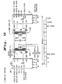
DLT 36 comprises adigital interface portion 64 for interfacing with thePABX 10 in a master operating mode and with the codec/filter 32 and subscriber data processor in a slave operating mode, a modulator/demodulator portion 66 for transmitting and receiving digital data words via the subscriber line, and a sequencer andcontrol portion 68 for controlling the sequence of operations performed by the digital interface and modulator/demodulator portions - In the
digital interface portion 64, a receive (RX)control circuit 70 responds to either of two channel receive enable signals, RE1 and RE2, by enabling a receive (RX) register 72 of the shift register type to serially receive digital data bits via a receive (RX) terminal in synchronization with a receive data clock (RDC) on a CLK/RDC terminal. When a predetermined "frame" of data (see discussion below) has been received, the sequencer andcontrol portion 68 enables theRX register 72 to transfer the "transmit" frame of data in parallel into a transmitter (XMIT) register 74 in the modulator/demodulator portion 66. Simultaneously, the then-current states of the two channel signalling bits on respective S11 and S21 terminals are latched and inserted into the frame of data in theXMIT register 74. Substantially independently, the sequencer andcontrol portion 68 enables a transmit (TX) register 76 to receive a "receive" frame of data in parallel from a receiver (RCV) register 78 in the modulator/demodulator portion 66. Simultaneously, the two channel signalling bits in the receive frame of data are latched and outputted on respective S10 and S20 terminals. In response to either of two channel transmit enable signals, TE1 and TE2, a transmit (TX)control circuit 80 enables the TX register 76 to serially transmit the receive frame of data via a TX terminal in synchronization with a transmit data clock (TDC) on an X1/TDC terminal. - In the modulator/
demodulator portion 66, a digital to analog converter (DAC)control circuit 82 periodically enables a digital to analog converter (DAC) 84 to transmit the transmit frame of data in the XMIT register 74 to the transmittransformer 40 in the subscriberline interface network 38 using a differential pair ofoutput drivers 86 and 88 coupled to respective line output terminals L01 and L02. In the preferred embodiment, theDAC 84 utilizes a burst differential phase shift keyed (DPSK) modulation technique at a carrier frequency of 265 kHz. Substantially independently, aninput buffer 90 of the differential to single ended output type in the modulation/demodulation portion 66 couples the signal received from the receivetransformer 42 in the subscriberline interface network 38 via line input terminals LI1 and LI2 to async detector 92 via awindow detector 94 and to acorrelator 96 via acomparator 98. As phase shifts of the proper form are decoded by thecorrelator 96, the "decoded" bits are shifted into a shift register portion thereof which maintains the most recently received set of data bits which might constitute a frame. When the energy of a DPSK signal of the proper frame length is detected, thesync detector 92 provides a valid sync signal to enable thecorrelator 96 to transfer the receive frame of data bits being maintained therein, in parallel to theRCV register 78. A switchedcapacitor bandgap reference 100 similar to that shown and described in WO-A-82/02806 provides a precision reference voltage to theDAC 84, thewindow detector 94, and thecomparator 98. Periodically, the offsets of theinput buffer 90, thewindow detector 94, thecomparator 98, and thebandgap reference 100 are zeroed by an auto-zerocircuit 102 in a manner similar to that shown and described in WO-A-82/02804. - In operation, the
DLT 36 provides duplex communication of digital data words on a pair of independent channels and a signalling bit associated with each of the channels, between the duplex subscriber line and a digital data port. In a typical line transmission operation, theRX register 72 successively receives a digital data word for each of the channels in synchronization with the receive data clock, with the digital data word for the first of the channels being received from the digital I/0 port via the RX terminal in response to the first of the channel receive enable signals, RE1, and the digital data word for the second of the channels being received from the digital I/O port via the RX terminal in response to the second of the channel receive enable signals, RE2. After the last data bit of the frame has been clocked into theRX register 72, both data words are transferred to theXMIT register 74, and the then-current states of the respective channel signalling bits on the S11 and S21 terminals added to complete the frame. As soon as the frame has been assembled, theDAC control circuit 82 actuates theDAC 84 to serially modulate the first and second digital data words and the respective channel signalling bits in the frame, for transmission via the transmittransformer 40 to one of the pairs of wires in the subscriber line. - In a typical line reception operation, the
sync detector 92 monitors the signal received via the receivetransformer 42 on the other pair of wires in the subscriber line, and provides a valid sync signal in response to detecting the energy of a DPSK modulated signal of the proper frame length. Meanwhile, thecorrelator 96 has been serially demodulating the sequentially received bits which might constitute a frame containing a digital data word for each of the channels and the respective channel signalling bits. In response to the valid sync signal, indicating that a valid frame has indeed been received, thecorrelator 96 transfers the frame to theRCVR register 78. At an appropriate time depending upon the mode of operation, the frame is then transferred from theRCVR register 78 to theTX register 76 and the respective channel signalling bits latched for output on the S10 and S20 terminals. The TX register 76 then sequentially transmits the digital data words in synchronization with the transmit data clock, with the digital data word for the first channel being transmitted to the digital I/O port via the TX terminal in response to the first of the channel transmit enable signals, TE1, and the digital data word for the second channel being transmitted to the digital I/O port via the TX terminal in response to the second of the channel transmit enable signals, TE2. - Shown in Figure 6 is a schematic representation of a 4-wire or duplex subscriber line which has been coupled at the exchange end thereof to the
DLT 36 in the digital line card 22' via the transmit and receivetransformers - In the digital line card 22' shown in Figure 3, the
DLT 36 is placed in the master mode of operation by a logic high signal on a master/slave (M/S) terminal. In the master mode, theDLT 36 emulates the codec/filter 32 with respect to the backplane by receiving/transmitting the digital data words just like the codec/filter 32, and by responding to the various control signals just like the codec/filter 32. In particular, theRX register 72 successively receives a digital data word for each of the channels in synchronization with the data clock provided by thePABX 10 via the backplane, with the data word for the first channel being received from the backplane via the RX terminal in response to the RE1 signal provided by a respective one of theTSACs 30 during the receive time slot assigned to the first channel, and the data word for the second channel being received from the backplane via the RX terminal in response to the RE2 signal provided by theother TSAC 30 during the receive time slot assigned to the second channel. In response to the next master sync input (MSI) received via an X2/MSI terminal after the last data bit of the frame has been clocked into theRX register 72, both digital data words are transferred to theXMIT register 74, and the then-current states of the respective channel signalling bits provided via the S11 and S21 terminals by theTSACs 30, respectively, added to complete the frame. As soon as the frame has been assembled, theDAC control circuit 82 actuates theDAC 84 to serially modulate the first and second digital data words and the respective channel signalling bits in the frame, for transmission via the transmittransformer 40 to the receive pair of wires in the subscriber line. - Simultaneously, the
sync detector 92 monitors the signal received via the receivetransformer 42 on the transmit pair of wires in the subscriber line, and provides the valid sync signal in response to detecting the energy of a DPSK modulated signal of the proper frame length. Meanwhile, thecorrelator 96 has been serially demodulating the sequentially received bits which might constitute a frame containing a digital data word for each of the channels and the respective channel signalling bits. In response to the valid sync signal, indicating that a valid frame has indeed been received, thecorrelator 96 transfers the frame to theRCVR register 78. In response to the next MSI, the frame is then transferred from theRCVR register 78 to theTX register 76 and the respective channel signalling bits latched for output on the S10 and S20 terminals. The TX register 76 then sequentially transmits the digital data words in synchronization with the transmit data clock provided by thePABX 10 via the backplane, with the digital data word for the first channel being transmitted to the backplane via the TX terminal in response to the TE1 signal provided by the first one of theTSACs 30 during the transmit time slot assigned to the first channel, and the digital data word for the second data channel being transmitted to the backplane via the TX terminal in response to the TE2 signal provided by theother TSAC 30 during the transmit time slot assigned to the second channel. A typical sequential interaction of theDLT 36 with theTSACs 30, and with thePABX 10 is illustrated by way of example in the timing diagram of Figure 7. - In the subscriber set 44 shown in Figure 4, the DLT 36' is placed in the slave mode of operation by a logic low on the master/slave (M/S) terminal. In the slave mode, the DLT 36' emulates the functions of the
TSAC 30 and the backplane with respect to the codec/filter 32' by providing the digital PCM voice data words and control signals necessary for the codec/filter 32' to operate, and by receiving the digital PCM voice data words provided by the codec/filter 32' just like the backplane. In this mode, thesync detector 92 monitors the signal received via the receive transformer 42' on the receive pair of wires in the subscriber line, and provides the valid sync signal in response to detecting the energy of a DPSK modulated signal of the proper frame length. Meanwhile, thecorrelator 96 has been serially demodulating the sequentially received bits which might constitute a frame containing a digital data word for each of the channels and the respective channel signalling bits. In response to the valid sync signal, indicating that a valid frame has indeed been received, thecorrelator 96 transfers the frame to theRCVR register 78. The frame is then promptly transferred from theRCVR register 78 to theTX register 76 and the respective channel signalling bits latched for output on the S10 and S20 terminals. The TX register 76 then sequentially transmits the digital data words in synchronization with a transmit data clock generated by a prescaler andoscillator 104 using a crystal coupled between the X1/TDC and X2/MSI terminals, with the digital data word for the first channel being transmitted to the codec/filter 32' via the TX terminal in synchronization with a TE1 signal generated by theTX control 80 relative to the last valid sync signal, and the digital data word for the second data channel being transmitted to thedata port 48 via the TX terminal in synchronization with a TE2 signal generated by theTX control 80 relative to the last valid sync signal. - In response to each of the valid sync signals provided by the
sync detector 92, theRX register 72 successively receives a digital data word for each of the channels in synchronization with a receive data clock generated by the sequencer andcontrol 68, with the digital PCM voice data word for the first channel being received from the codec/filter 32' via the RX terminal in synchronization with an RE1 signal generated by theRX control 70 relative to the last valid sync signal, and the digital data word for the second channel being received from thedata port 48 via the RX terminal in response to an RE2 signal generated by theRX control 70 relative to the last valid sync signal. In response to the next valid sync signal provided by thesync detector 92, both digital data words are transferred to theXMIT register 74 and the then-current states of the respective channel signalling bits provided via the S11 and S21 terminals by thehook switch 58 and, if appropriate, the subscriber data processor, respectively, are added to complete the frame. As soon as the frame has been assembled, theDAC control circuit 82 actuates theDAC 84 to serially modulate the first and second digital data words and the respective channel signalling bits in the frame, for transmission via the transmit transformer 40' to the transmit pair of wires in the subscriber line. A typical sequential interaction of the DLT 36' with the codec/filter 32' and the subscriber data processor is illustrated by way of example in the timing diagram of Figure 8. - Although the
DLT 36 is designed to operate primarily in the dual-channel mode over a duplex subscriber line, theDLT 36 may be operated in an exchange which has only one pair of wires in each subscriber line by applying a logic high to a format (FOR) terminal thereof. In the illustrated form of such a 2-wire system shown in Figure 9, the half duplex subscriber line is coupled at the exchange end thereof to theDLT 36 in the digital line card 22' via a transmit/receiveisolation transformer 106, and at the subscriber end thereof to the DLT 36' in the digital subscriber set 44 via a transmit/receive isolation transformer 106'. In the dual-channel form of the half duplex system, a frame of data comprises an 8-bit digital data word for the first channel, the signalling bit for the first channel, and a second signalling bit for use by the subscriber data processor as a digital data bit. Preferably, the frame also includes a parity bit, either even or odd, as desired. A suitable frame format is illustrated in Figure 9. Since only a single digital data bit may be transferred in each frame, the effective data bit transmission rate is only 8 kHz rather than the 64 kHz of the duplex system. However, this reduced data rate may be acceptable in situations where the cost to install the second pair of wires in the subscriber line outweighs the benefits of higher transmission rate.
Claims (3)
Applications Claiming Priority (2)
| Application Number | Priority Date | Filing Date | Title |
|---|---|---|---|
| US06/334,412 US4432089A (en) | 1981-12-24 | 1981-12-24 | Digital loop transceiver for interfacing a digital PABX to a digital subscriber set via a subscriber line |
| US334412 | 1981-12-24 |
Publications (3)
| Publication Number | Publication Date |
|---|---|
| EP0097166A1 EP0097166A1 (en) | 1984-01-04 |
| EP0097166A4 EP0097166A4 (en) | 1984-05-29 |
| EP0097166B1 true EP0097166B1 (en) | 1988-01-27 |
Family
ID=23307090
Family Applications (1)
| Application Number | Title | Priority Date | Filing Date |
|---|---|---|---|
| EP82903416A Expired EP0097166B1 (en) | 1981-12-24 | 1982-10-04 | Digital loop transceiver for interfacing a digital pabx to a digital subscriber set via a subscriber line |
Country Status (7)
| Country | Link |
|---|---|
| US (1) | US4432089A (en) |
| EP (1) | EP0097166B1 (en) |
| JP (1) | JPS59500037A (en) |
| CA (1) | CA1187969A (en) |
| DE (1) | DE3278065D1 (en) |
| HK (1) | HK65290A (en) |
| WO (1) | WO1983002379A1 (en) |
Families Citing this family (39)
| Publication number | Priority date | Publication date | Assignee | Title |
|---|---|---|---|---|
| EP0103324A3 (en) * | 1982-09-10 | 1984-07-18 | Motorola, Inc. | Simultaneous voice and data transmission circuit having a digital loop transceiver |
| US4510596A (en) * | 1982-10-12 | 1985-04-09 | At&T Bell Labs | Time slot assignment facilities |
| US4535453A (en) * | 1982-12-27 | 1985-08-13 | Siemens Corporate Research & Support, Inc. | Signaling input/output processing module for a telecommunication system |
| JPH0667019B2 (en) * | 1983-08-12 | 1994-08-24 | 株式会社東芝 | Switch control system |
| US4569062A (en) * | 1984-06-28 | 1986-02-04 | Dellande Brian W | Interface circuit for interfacing between asynchronous data in start/stop format and synchronous data |
| GB8430003D0 (en) * | 1984-11-28 | 1985-01-09 | Plessey Co Plc | Subscriber line interface modem |
| US4646288A (en) * | 1985-01-31 | 1987-02-24 | Denro Laboratories, Inc. | Multi-line accumulator/multiplexer |
| JPH0652896B2 (en) * | 1986-03-20 | 1994-07-06 | 沖電気工業株式会社 | Start control method |
| US4813066A (en) * | 1987-07-13 | 1989-03-14 | American Telephone And Telegraph Company, At&T Information Systems | Battery feed circuit for a telephone system |
| NL8800124A (en) * | 1988-01-20 | 1989-08-16 | Philips Nv | METHOD FOR ASYNCHRONOUS DUPLEX DATA COMMUNICATION BETWEEN TWO STATIONS CONCERNING CERTAIN SERVICES AND STATION TO BE IMPLEMENTED THROUGH A COMMON COMMUNICATION CHANNEL FOR CARRYING OUT THIS METHOD. |
| US5022047A (en) * | 1989-08-07 | 1991-06-04 | Omnipoint Data Corporation | Spread spectrum correlator |
| US5016255A (en) * | 1989-08-07 | 1991-05-14 | Omnipoint Data Company, Incorporated | Asymmetric spread spectrum correlator |
| US5499265A (en) * | 1989-08-07 | 1996-03-12 | Omnipoint Data Company, Incorporated | Spread spectrum correlator |
| JPH05509213A (en) * | 1990-07-23 | 1993-12-16 | オムニポイント・コーポレイション | SAWC phase detection method and device |
| US5081642A (en) * | 1990-08-06 | 1992-01-14 | Omnipoint Data Company, Incorporated | Reciprocal saw correlator method and apparatus |
| WO1992007434A1 (en) * | 1990-10-23 | 1992-04-30 | Omnipoint Corporation | Method and apparatus for establishing spread spectrum communications |
| US5283827A (en) * | 1990-11-19 | 1994-02-01 | Ag Communication Systems Corporation | Digital line card for interfacing a remotely located digital telephone to a central office system |
| US5402413A (en) * | 1991-04-08 | 1995-03-28 | Omnipoint Corporation | Three-cell wireless communication system |
| US5790587A (en) * | 1991-05-13 | 1998-08-04 | Omnipoint Corporation | Multi-band, multi-mode spread-spectrum communication system |
| US5796772A (en) * | 1991-05-13 | 1998-08-18 | Omnipoint Corporation | Multi-band, multi-mode spread-spectrum communication system |
| US5887020A (en) * | 1991-05-13 | 1999-03-23 | Omnipoint Corporation | Multi-band, multi-mode spread-spectrum communication system |
| US5815525A (en) * | 1991-05-13 | 1998-09-29 | Omnipoint Corporation | Multi-band, multi-mode spread-spectrum communication system |
| US5694414A (en) * | 1991-05-13 | 1997-12-02 | Omnipoint Corporation | Multi-band, multi-mode spread-spectrum communication system |
| WO1992021195A1 (en) * | 1991-05-13 | 1992-11-26 | Omnipoint Corporation | Dual mode transmitter and receiver |
| US5285469A (en) * | 1991-06-03 | 1994-02-08 | Omnipoint Data Corporation | Spread spectrum wireless telephone system |
| JP3766434B2 (en) * | 1991-12-16 | 2006-04-12 | ザーカム ワイヤレス, インコーポレイテッド | Spread spectrum data transmission system |
| US5355389A (en) * | 1993-01-13 | 1994-10-11 | Omnipoint Corporation | Reciprocal mode saw correlator method and apparatus |
| US6005856A (en) * | 1993-11-01 | 1999-12-21 | Omnipoint Corporation | Communication protocol for spread spectrum wireless communication system |
| US6094575A (en) * | 1993-11-01 | 2000-07-25 | Omnipoint Corporation | Communication system and method |
| US6088590A (en) * | 1993-11-01 | 2000-07-11 | Omnipoint Corporation | Method and system for mobile controlled handoff and link maintenance in spread spectrum communication |
| US5689502A (en) * | 1995-06-05 | 1997-11-18 | Omnipoint Corporation | Efficient frequency division duplex communication system with interleaved format and timing adjustment control |
| US5745484A (en) * | 1995-06-05 | 1998-04-28 | Omnipoint Corporation | Efficient communication system using time division multiplexing and timing adjustment control |
| US6356607B1 (en) | 1995-06-05 | 2002-03-12 | Omnipoint Corporation | Preamble code structure and detection method and apparatus |
| US5959980A (en) * | 1995-06-05 | 1999-09-28 | Omnipoint Corporation | Timing adjustment control for efficient time division duplex communication |
| US5802046A (en) * | 1995-06-05 | 1998-09-01 | Omnipoint Corporation | Efficient time division duplex communication system with interleaved format and timing adjustment control |
| US6041046A (en) * | 1995-07-14 | 2000-03-21 | Omnipoint Corporation | Cyclic time hopping in time division multiple access communication system |
| US6141373A (en) | 1996-11-15 | 2000-10-31 | Omnipoint Corporation | Preamble code structure and detection method and apparatus |
| US6947469B2 (en) | 1999-05-07 | 2005-09-20 | Intel Corporation | Method and Apparatus for wireless spread spectrum communication with preamble processing period |
| JP3821740B2 (en) * | 2002-03-22 | 2006-09-13 | Necインフロンティア株式会社 | Audio data transmitter / receiver |
Citations (1)
| Publication number | Priority date | Publication date | Assignee | Title |
|---|---|---|---|---|
| US3665328A (en) * | 1969-07-02 | 1972-05-23 | Ericsson Telefon Ab L M | Synchronizing signal generator for use with a differentially multiphase modulated signal receiver |
Family Cites Families (7)
| Publication number | Priority date | Publication date | Assignee | Title |
|---|---|---|---|---|
| US3924077A (en) * | 1973-07-05 | 1975-12-02 | Thomas R Blakeslee | Pulse code modulation time division multiplex telephone system |
| GB1479009A (en) * | 1974-07-12 | 1977-07-06 | Sarma B | Telecommunication switching system |
| DE2643687C2 (en) * | 1976-09-28 | 1983-09-29 | Siemens AG, 1000 Berlin und 8000 München | Circuit arrangement for the transmission of digital signals between subscriber stations of a time division multiplex telecommunications network, in particular PCM time division multiplex telecommunications network |
| DE2819119C3 (en) * | 1978-04-29 | 1980-10-30 | Telefonbau Und Normalzeit Gmbh, 6000 Frankfurt | Circuit arrangement for time-division multiplex digitally switching telecommunication systems, in particular telephone switching systems |
| CA1123102A (en) * | 1979-07-27 | 1982-05-04 | Harold H. Harris | Line interface unit for voice and wide band signal coupling |
| DE3010702C2 (en) * | 1980-03-20 | 1982-11-04 | Standard Elektrik Lorenz Ag, 7000 Stuttgart | Digital messaging system |
| US4450556A (en) * | 1980-10-17 | 1984-05-22 | Northern Telecom Limited | Digital signal subscriber loop and interface circuit |
-
1981
- 1981-12-24 US US06/334,412 patent/US4432089A/en not_active Expired - Lifetime
-
1982
- 1982-10-04 JP JP82503422A patent/JPS59500037A/en active Pending
- 1982-10-04 WO PCT/US1982/001435 patent/WO1983002379A1/en active IP Right Grant
- 1982-10-04 DE DE8282903416T patent/DE3278065D1/en not_active Expired
- 1982-10-04 EP EP82903416A patent/EP0097166B1/en not_active Expired
- 1982-10-25 CA CA000414134A patent/CA1187969A/en not_active Expired
-
1990
- 1990-08-23 HK HK652/90A patent/HK65290A/en not_active IP Right Cessation
Patent Citations (1)
| Publication number | Priority date | Publication date | Assignee | Title |
|---|---|---|---|---|
| US3665328A (en) * | 1969-07-02 | 1972-05-23 | Ericsson Telefon Ab L M | Synchronizing signal generator for use with a differentially multiphase modulated signal receiver |
Non-Patent Citations (5)
| Title |
|---|
| ELECTRICAL DESIGN NEWS, June 10, 1981, DENVER (US)N.WELLENSTEIN: "Digital ICs switch analog phones for high performance, low cost"", pages 131-136 * |
| ELECTRONICS INTERNATIONAL, vol. 55, no. 19, September 22, 1982, NEW YORK (US) H. WURZBURG et al.: "C-MOS chip set gives new life to twisted pairs for local networks", pages 125-130 * |
| IEEE INTERNATIONAL SOLID-STATE CIRCUITS CONFERENCE, February 14, 1980, NEW YORK (US) A. BOLEDA: "A monolothic digital line interface circuit", pages 176-177 * |
| INTERNATIONAL SWITCHING SYMPOSIUM, session 41C, pager 5, September 21-25, 1981, MONTREAL (CA) WONG et al.: "Switched multi-channel access to the integrated services digital network", pages 1-7 * |
| Patent Abstracts of Japan, Vol. 5, Number 86 (E-60), (758), June 05, 1981; English abstract of JP-A-56-32847 * |
Also Published As
| Publication number | Publication date |
|---|---|
| JPS59500037A (en) | 1984-01-05 |
| DE3278065D1 (en) | 1988-03-03 |
| WO1983002379A1 (en) | 1983-07-07 |
| EP0097166A1 (en) | 1984-01-04 |
| HK65290A (en) | 1990-08-31 |
| EP0097166A4 (en) | 1984-05-29 |
| CA1187969A (en) | 1985-05-28 |
| US4432089A (en) | 1984-02-14 |
Similar Documents
| Publication | Publication Date | Title |
|---|---|---|
| EP0097166B1 (en) | Digital loop transceiver for interfacing a digital pabx to a digital subscriber set via a subscriber line | |
| US4484028A (en) | Digital loop transceiver having a power up/down circuit | |
| US4593389A (en) | Simultaneous voice and asynchronous data telephone | |
| US4423507A (en) | Communications system for interconnecting a plurality of asynchronous data processing terminals | |
| EP0161300B1 (en) | Multimode data communication system | |
| EP0607250B1 (en) | Digital wireless interface | |
| US4779262A (en) | Connection of subscriber communication network base station to external information network | |
| CA2055828C (en) | Arbitrary selecting of a terminal to be called in key telephone systems | |
| CA2037557A1 (en) | Method for in-house voice and data communication through the in-house power supply | |
| EP0103324A2 (en) | Simultaneous voice and data transmission circuit having a digital loop transceiver | |
| EP0741950A1 (en) | Ct2 telephone system | |
| JPS59115699A (en) | Digital exchange | |
| JP3451052B2 (en) | Communication system using data signal multiplexing system | |
| JPH0210713Y2 (en) | ||
| KR0128170B1 (en) | Method and connection device for telephone | |
| WO1995005719A1 (en) | Method and equipment for adapting ct2 calls for an isdn subscriber line | |
| JP2547126B2 (en) | TDMA mobile communication terminal | |
| JPS62157442A (en) | Composite terminal equipment for isdn | |
| JPH0965408A (en) | Personal handy phone system using catv network and its communication method | |
| KR100251584B1 (en) | Data transmission apparatus for a dect radio communication system | |
| KR960013266B1 (en) | Modem data communication | |
| KR100284319B1 (en) | Time Switch Stabilization Circuit of Aerial Network Matching Device in Satellite Communication System | |
| JPS6128252A (en) | Transmitter possible for extension transfer | |
| KR19980053444A (en) | Transmission distance extension device of S interface in premises NISDN service | |
| JPH05252311A (en) | Switched network modulator/demodulator with multi-address function |
Legal Events
| Date | Code | Title | Description |
|---|---|---|---|
| PUAI | Public reference made under article 153(3) epc to a published international application that has entered the european phase |
Free format text: ORIGINAL CODE: 0009012 |
|
| 17P | Request for examination filed |
Effective date: 19830825 |
|
| AK | Designated contracting states |
Designated state(s): DE FR GB NL SE |
|
| GRAA | (expected) grant |
Free format text: ORIGINAL CODE: 0009210 |
|
| AK | Designated contracting states |
Kind code of ref document: B1 Designated state(s): DE FR GB NL SE |
|
| PG25 | Lapsed in a contracting state [announced via postgrant information from national office to epo] |
Ref country code: NL Effective date: 19880127 |
|
| PG25 | Lapsed in a contracting state [announced via postgrant information from national office to epo] |
Ref country code: SE Effective date: 19880131 |
|
| REF | Corresponds to: |
Ref document number: 3278065 Country of ref document: DE Date of ref document: 19880303 |
|
| ET | Fr: translation filed | ||
| NLV1 | Nl: lapsed or annulled due to failure to fulfill the requirements of art. 29p and 29m of the patents act | ||
| PLBE | No opposition filed within time limit |
Free format text: ORIGINAL CODE: 0009261 |
|
| STAA | Information on the status of an ep patent application or granted ep patent |
Free format text: STATUS: NO OPPOSITION FILED WITHIN TIME LIMIT |
|
| 26N | No opposition filed | ||
| PGFP | Annual fee paid to national office [announced via postgrant information from national office to epo] |
Ref country code: GB Payment date: 19970930 Year of fee payment: 16 |
|
| PGFP | Annual fee paid to national office [announced via postgrant information from national office to epo] |
Ref country code: FR Payment date: 19971015 Year of fee payment: 16 |
|
| PGFP | Annual fee paid to national office [announced via postgrant information from national office to epo] |
Ref country code: DE Payment date: 19971023 Year of fee payment: 16 |
|
| PG25 | Lapsed in a contracting state [announced via postgrant information from national office to epo] |
Ref country code: GB Free format text: LAPSE BECAUSE OF NON-PAYMENT OF DUE FEES Effective date: 19981004 |
|
| GBPC | Gb: european patent ceased through non-payment of renewal fee |
Effective date: 19981004 |
|
| PG25 | Lapsed in a contracting state [announced via postgrant information from national office to epo] |
Ref country code: FR Free format text: LAPSE BECAUSE OF NON-PAYMENT OF DUE FEES Effective date: 19990630 |
|
| REG | Reference to a national code |
Ref country code: FR Ref legal event code: ST |
|
| PG25 | Lapsed in a contracting state [announced via postgrant information from national office to epo] |
Ref country code: DE Free format text: LAPSE BECAUSE OF NON-PAYMENT OF DUE FEES Effective date: 19990803 |