EP0162349A2 - A data recording medium - Google Patents
A data recording medium Download PDFInfo
- Publication number
- EP0162349A2 EP0162349A2 EP85105240A EP85105240A EP0162349A2 EP 0162349 A2 EP0162349 A2 EP 0162349A2 EP 85105240 A EP85105240 A EP 85105240A EP 85105240 A EP85105240 A EP 85105240A EP 0162349 A2 EP0162349 A2 EP 0162349A2
- Authority
- EP
- European Patent Office
- Prior art keywords
- layer
- magnetic recording
- disk
- patterned
- accordance
- Prior art date
- Legal status (The legal status is an assumption and is not a legal conclusion. Google has not performed a legal analysis and makes no representation as to the accuracy of the status listed.)
- Withdrawn
Links
- 230000005291 magnetic effect Effects 0.000 claims abstract description 139
- 239000011241 protective layer Substances 0.000 claims abstract description 55
- 239000000463 material Substances 0.000 claims abstract description 40
- 229910052751 metal Inorganic materials 0.000 claims abstract description 20
- 239000002184 metal Substances 0.000 claims abstract description 20
- 229910052782 aluminium Inorganic materials 0.000 claims abstract description 18
- 229910052710 silicon Inorganic materials 0.000 claims abstract description 11
- 239000010409 thin film Substances 0.000 claims abstract description 8
- 230000008021 deposition Effects 0.000 claims abstract description 5
- 239000010410 layer Substances 0.000 claims description 154
- 239000000758 substrate Substances 0.000 claims description 19
- 239000011651 chromium Substances 0.000 claims description 16
- 238000005530 etching Methods 0.000 claims description 16
- 229910052804 chromium Inorganic materials 0.000 claims description 13
- VYPSYNLAJGMNEJ-UHFFFAOYSA-N Silicium dioxide Chemical compound O=[Si]=O VYPSYNLAJGMNEJ-UHFFFAOYSA-N 0.000 claims description 11
- XAGFODPZIPBFFR-UHFFFAOYSA-N aluminium Chemical compound [Al] XAGFODPZIPBFFR-UHFFFAOYSA-N 0.000 claims description 11
- VYZAMTAEIAYCRO-UHFFFAOYSA-N Chromium Chemical compound [Cr] VYZAMTAEIAYCRO-UHFFFAOYSA-N 0.000 claims description 6
- 239000000377 silicon dioxide Substances 0.000 claims description 5
- 235000012239 silicon dioxide Nutrition 0.000 claims description 5
- TWNQGVIAIRXVLR-UHFFFAOYSA-N oxo(oxoalumanyloxy)alumane Chemical compound O=[Al]O[Al]=O TWNQGVIAIRXVLR-UHFFFAOYSA-N 0.000 claims description 4
- 229910052715 tantalum Inorganic materials 0.000 claims description 4
- 229910052719 titanium Inorganic materials 0.000 claims description 2
- GWEVSGVZZGPLCZ-UHFFFAOYSA-N Titan oxide Chemical compound O=[Ti]=O GWEVSGVZZGPLCZ-UHFFFAOYSA-N 0.000 claims 2
- 230000001050 lubricating effect Effects 0.000 claims 2
- 239000007769 metal material Substances 0.000 claims 2
- 239000010703 silicon Substances 0.000 claims 2
- GUVRBAGPIYLISA-UHFFFAOYSA-N tantalum atom Chemical compound [Ta] GUVRBAGPIYLISA-UHFFFAOYSA-N 0.000 claims 2
- RTAQQCXQSZGOHL-UHFFFAOYSA-N Titanium Chemical compound [Ti] RTAQQCXQSZGOHL-UHFFFAOYSA-N 0.000 claims 1
- 229940090961 chromium dioxide Drugs 0.000 claims 1
- IAQWMWUKBQPOIY-UHFFFAOYSA-N chromium(4+);oxygen(2-) Chemical compound [O-2].[O-2].[Cr+4] IAQWMWUKBQPOIY-UHFFFAOYSA-N 0.000 claims 1
- AYTAKQFHWFYBMA-UHFFFAOYSA-N chromium(IV) oxide Inorganic materials O=[Cr]=O AYTAKQFHWFYBMA-UHFFFAOYSA-N 0.000 claims 1
- 239000003989 dielectric material Substances 0.000 claims 1
- NQKXFODBPINZFK-UHFFFAOYSA-N dioxotantalum Chemical compound O=[Ta]=O NQKXFODBPINZFK-UHFFFAOYSA-N 0.000 claims 1
- 239000010936 titanium Substances 0.000 claims 1
- 239000004408 titanium dioxide Substances 0.000 claims 1
- 238000000034 method Methods 0.000 abstract description 37
- 238000007254 oxidation reaction Methods 0.000 abstract description 18
- 230000003647 oxidation Effects 0.000 abstract description 17
- 230000003287 optical effect Effects 0.000 abstract description 12
- 238000003860 storage Methods 0.000 abstract description 6
- 238000000992 sputter etching Methods 0.000 abstract description 3
- 150000002739 metals Chemical class 0.000 abstract description 2
- 238000005121 nitriding Methods 0.000 abstract description 2
- 238000001228 spectrum Methods 0.000 abstract description 2
- 230000007547 defect Effects 0.000 description 11
- 239000010408 film Substances 0.000 description 11
- 239000000314 lubricant Substances 0.000 description 11
- 238000012986 modification Methods 0.000 description 7
- 230000004048 modification Effects 0.000 description 7
- 239000002344 surface layer Substances 0.000 description 7
- OKTJSMMVPCPJKN-UHFFFAOYSA-N Carbon Chemical compound [C] OKTJSMMVPCPJKN-UHFFFAOYSA-N 0.000 description 6
- 238000002048 anodisation reaction Methods 0.000 description 6
- 229910052799 carbon Inorganic materials 0.000 description 6
- 229920002120 photoresistant polymer Polymers 0.000 description 6
- 229910000684 Cobalt-chrome Inorganic materials 0.000 description 5
- 239000010952 cobalt-chrome Substances 0.000 description 5
- 230000000873 masking effect Effects 0.000 description 5
- UQSXHKLRYXJYBZ-UHFFFAOYSA-N Iron oxide Chemical compound [Fe]=O UQSXHKLRYXJYBZ-UHFFFAOYSA-N 0.000 description 4
- 238000013500 data storage Methods 0.000 description 4
- MUBZPKHOEPUJKR-UHFFFAOYSA-N Oxalic acid Chemical compound OC(=O)C(O)=O MUBZPKHOEPUJKR-UHFFFAOYSA-N 0.000 description 3
- 239000004642 Polyimide Substances 0.000 description 3
- HEMHJVSKTPXQMS-UHFFFAOYSA-M Sodium hydroxide Chemical compound [OH-].[Na+] HEMHJVSKTPXQMS-UHFFFAOYSA-M 0.000 description 3
- 229910045601 alloy Inorganic materials 0.000 description 3
- 239000000956 alloy Substances 0.000 description 3
- 239000007864 aqueous solution Substances 0.000 description 3
- 239000011248 coating agent Substances 0.000 description 3
- 238000000576 coating method Methods 0.000 description 3
- 230000007797 corrosion Effects 0.000 description 3
- 238000005260 corrosion Methods 0.000 description 3
- 238000000151 deposition Methods 0.000 description 3
- NBVXSUQYWXRMNV-UHFFFAOYSA-N fluoromethane Chemical compound FC NBVXSUQYWXRMNV-UHFFFAOYSA-N 0.000 description 3
- 229920001721 polyimide Polymers 0.000 description 3
- 239000000243 solution Substances 0.000 description 3
- 239000002904 solvent Substances 0.000 description 3
- CSCPPACGZOOCGX-UHFFFAOYSA-N Acetone Chemical compound CC(C)=O CSCPPACGZOOCGX-UHFFFAOYSA-N 0.000 description 2
- 229910052581 Si3N4 Inorganic materials 0.000 description 2
- 230000002411 adverse Effects 0.000 description 2
- 125000004429 atom Chemical group 0.000 description 2
- QVGXLLKOCUKJST-UHFFFAOYSA-N atomic oxygen Chemical compound [O] QVGXLLKOCUKJST-UHFFFAOYSA-N 0.000 description 2
- 150000001540 azides Chemical class 0.000 description 2
- 230000015572 biosynthetic process Effects 0.000 description 2
- 238000003486 chemical etching Methods 0.000 description 2
- 230000000694 effects Effects 0.000 description 2
- 238000010894 electron beam technology Methods 0.000 description 2
- 230000008020 evaporation Effects 0.000 description 2
- 238000001704 evaporation Methods 0.000 description 2
- 229910052741 iridium Inorganic materials 0.000 description 2
- 229910052762 osmium Inorganic materials 0.000 description 2
- 229910052760 oxygen Inorganic materials 0.000 description 2
- 239000001301 oxygen Substances 0.000 description 2
- 229920000642 polymer Polymers 0.000 description 2
- 238000012545 processing Methods 0.000 description 2
- 230000002441 reversible effect Effects 0.000 description 2
- 239000010948 rhodium Substances 0.000 description 2
- 239000007787 solid Substances 0.000 description 2
- 238000004544 sputter deposition Methods 0.000 description 2
- 239000000126 substance Substances 0.000 description 2
- 230000003746 surface roughness Effects 0.000 description 2
- 238000012876 topography Methods 0.000 description 2
- IVRMZWNICZWHMI-UHFFFAOYSA-N Azide Chemical compound [N-]=[N+]=[N-] IVRMZWNICZWHMI-UHFFFAOYSA-N 0.000 description 1
- 229910018979 CoPt Inorganic materials 0.000 description 1
- 238000005033 Fourier transform infrared spectroscopy Methods 0.000 description 1
- 229910007277 Si3 N4 Inorganic materials 0.000 description 1
- 229910020489 SiO3 Inorganic materials 0.000 description 1
- 238000004833 X-ray photoelectron spectroscopy Methods 0.000 description 1
- 238000010521 absorption reaction Methods 0.000 description 1
- 239000000654 additive Substances 0.000 description 1
- 230000000996 additive effect Effects 0.000 description 1
- 238000012993 chemical processing Methods 0.000 description 1
- 229910052681 coesite Inorganic materials 0.000 description 1
- 238000010276 construction Methods 0.000 description 1
- 229910052906 cristobalite Inorganic materials 0.000 description 1
- 230000007423 decrease Effects 0.000 description 1
- 230000002939 deleterious effect Effects 0.000 description 1
- 238000005137 deposition process Methods 0.000 description 1
- 238000001514 detection method Methods 0.000 description 1
- 239000011521 glass Substances 0.000 description 1
- 238000009499 grossing Methods 0.000 description 1
- 229910052735 hafnium Inorganic materials 0.000 description 1
- 229910052736 halogen Inorganic materials 0.000 description 1
- 150000002367 halogens Chemical class 0.000 description 1
- 229930195733 hydrocarbon Natural products 0.000 description 1
- 150000002430 hydrocarbons Chemical class 0.000 description 1
- 238000010348 incorporation Methods 0.000 description 1
- XEEYBQQBJWHFJM-UHFFFAOYSA-N iron Substances [Fe] XEEYBQQBJWHFJM-UHFFFAOYSA-N 0.000 description 1
- 238000001459 lithography Methods 0.000 description 1
- 239000010687 lubricating oil Substances 0.000 description 1
- 229910052749 magnesium Inorganic materials 0.000 description 1
- 239000000696 magnetic material Substances 0.000 description 1
- 238000004519 manufacturing process Methods 0.000 description 1
- 238000005259 measurement Methods 0.000 description 1
- 229910044991 metal oxide Inorganic materials 0.000 description 1
- 150000004706 metal oxides Chemical class 0.000 description 1
- 238000001465 metallisation Methods 0.000 description 1
- 229910052750 molybdenum Inorganic materials 0.000 description 1
- 229910052759 nickel Inorganic materials 0.000 description 1
- 235000006408 oxalic acid Nutrition 0.000 description 1
- 230000001590 oxidative effect Effects 0.000 description 1
- NDLPOXTZKUMGOV-UHFFFAOYSA-N oxo(oxoferriooxy)iron hydrate Chemical compound O.O=[Fe]O[Fe]=O NDLPOXTZKUMGOV-UHFFFAOYSA-N 0.000 description 1
- 125000004430 oxygen atom Chemical group O* 0.000 description 1
- 230000036961 partial effect Effects 0.000 description 1
- 239000002245 particle Substances 0.000 description 1
- 238000000059 patterning Methods 0.000 description 1
- 229920003229 poly(methyl methacrylate) Polymers 0.000 description 1
- 239000004926 polymethyl methacrylate Substances 0.000 description 1
- 230000001681 protective effect Effects 0.000 description 1
- 239000010453 quartz Substances 0.000 description 1
- 230000002829 reductive effect Effects 0.000 description 1
- 229910052703 rhodium Inorganic materials 0.000 description 1
- MHOVAHRLVXNVSD-UHFFFAOYSA-N rhodium atom Chemical compound [Rh] MHOVAHRLVXNVSD-UHFFFAOYSA-N 0.000 description 1
- 238000001878 scanning electron micrograph Methods 0.000 description 1
- HQVNEWCFYHHQES-UHFFFAOYSA-N silicon nitride Chemical compound N12[Si]34N5[Si]62N3[Si]51N64 HQVNEWCFYHHQES-UHFFFAOYSA-N 0.000 description 1
- 229910052682 stishovite Inorganic materials 0.000 description 1
- 229910052905 tridymite Inorganic materials 0.000 description 1
- 229910052721 tungsten Inorganic materials 0.000 description 1
- 229910052720 vanadium Inorganic materials 0.000 description 1
- 238000003631 wet chemical etching Methods 0.000 description 1
- 238000001039 wet etching Methods 0.000 description 1
- 229910052726 zirconium Inorganic materials 0.000 description 1
Images


Classifications
-
- G—PHYSICS
- G11—INFORMATION STORAGE
- G11B—INFORMATION STORAGE BASED ON RELATIVE MOVEMENT BETWEEN RECORD CARRIER AND TRANSDUCER
- G11B7/00—Recording or reproducing by optical means, e.g. recording using a thermal beam of optical radiation by modifying optical properties or the physical structure, reproducing using an optical beam at lower power by sensing optical properties; Record carriers therefor
- G11B7/08—Disposition or mounting of heads or light sources relatively to record carriers
- G11B7/09—Disposition or mounting of heads or light sources relatively to record carriers with provision for moving the light beam or focus plane for the purpose of maintaining alignment of the light beam relative to the record carrier during transducing operation, e.g. to compensate for surface irregularities of the latter or for track following
- G11B7/0938—Disposition or mounting of heads or light sources relatively to record carriers with provision for moving the light beam or focus plane for the purpose of maintaining alignment of the light beam relative to the record carrier during transducing operation, e.g. to compensate for surface irregularities of the latter or for track following servo format, e.g. guide tracks, pilot signals
-
- G—PHYSICS
- G11—INFORMATION STORAGE
- G11B—INFORMATION STORAGE BASED ON RELATIVE MOVEMENT BETWEEN RECORD CARRIER AND TRANSDUCER
- G11B23/00—Record carriers not specific to the method of recording or reproducing; Accessories, e.g. containers, specially adapted for co-operation with the recording or reproducing apparatus ; Intermediate mediums; Apparatus or processes specially adapted for their manufacture
- G11B23/30—Record carriers not specific to the method of recording or reproducing; Accessories, e.g. containers, specially adapted for co-operation with the recording or reproducing apparatus ; Intermediate mediums; Apparatus or processes specially adapted for their manufacture with provision for auxiliary signals
-
- G—PHYSICS
- G11—INFORMATION STORAGE
- G11B—INFORMATION STORAGE BASED ON RELATIVE MOVEMENT BETWEEN RECORD CARRIER AND TRANSDUCER
- G11B5/00—Recording by magnetisation or demagnetisation of a record carrier; Reproducing by magnetic means; Record carriers therefor
- G11B5/48—Disposition or mounting of heads or head supports relative to record carriers ; arrangements of heads, e.g. for scanning the record carrier to increase the relative speed
- G11B5/58—Disposition or mounting of heads or head supports relative to record carriers ; arrangements of heads, e.g. for scanning the record carrier to increase the relative speed with provision for moving the head for the purpose of maintaining alignment of the head relative to the record carrier during transducing operation, e.g. to compensate for surface irregularities of the latter or for track following
- G11B5/596—Disposition or mounting of heads or head supports relative to record carriers ; arrangements of heads, e.g. for scanning the record carrier to increase the relative speed with provision for moving the head for the purpose of maintaining alignment of the head relative to the record carrier during transducing operation, e.g. to compensate for surface irregularities of the latter or for track following for track following on disks
-
- G—PHYSICS
- G11—INFORMATION STORAGE
- G11B—INFORMATION STORAGE BASED ON RELATIVE MOVEMENT BETWEEN RECORD CARRIER AND TRANSDUCER
- G11B5/00—Recording by magnetisation or demagnetisation of a record carrier; Reproducing by magnetic means; Record carriers therefor
- G11B5/74—Record carriers characterised by the form, e.g. sheet shaped to wrap around a drum
- G11B5/82—Disk carriers
-
- G—PHYSICS
- G11—INFORMATION STORAGE
- G11B—INFORMATION STORAGE BASED ON RELATIVE MOVEMENT BETWEEN RECORD CARRIER AND TRANSDUCER
- G11B7/00—Recording or reproducing by optical means, e.g. recording using a thermal beam of optical radiation by modifying optical properties or the physical structure, reproducing using an optical beam at lower power by sensing optical properties; Record carriers therefor
- G11B7/24—Record carriers characterised by shape, structure or physical properties, or by the selection of the material
Definitions
- the present invention relates to data storage media and more particularly to patterning such media to provide servo control information on the media concurrently with maximum storage density and optimal accuracy of the servo system utilized to position the magnetic recording heads which read the data on the media.
- magnetic recording disk files have incorporated tracks for providing positioning information to a servo system which guides and controls the position of magnetic recording heads above the disk files as they search for the location where the data to be read is located.
- the servo system receives signals from a servo data sensor as it follows any selected one of a plurality of concentric magnetic recording tracks on the disk. Then the servo holds the head centered above such a selected recording track which contains data stored in the form of magnetic records on the disk files.
- Some magnetic disk files use a separate portion of the disk surface and a separate head (the servo head) on that surface for magnetically storing positioning information which provides the track location information followed by the servo system.
- the servo head On that surface, all other recording heads are mechanically ganged to the servo head so that when the electronic servo system holds the servo head centered above a servo track, all other recording heads are approximately centered above their respective data tracks.
- Another system of storing servo information on the magnetic disk is the "sector servo" system in which the servo information on the disk indicating track locations is stored in sectors of the disk file which are interspersed (i.e. inserted at spatial intervals along a circular track on the disk) around the surface of the disk. The servo information is stored between sectors in which data is stored.
- the advantage of the sector servo system is that the servo information is stored at the same track radius from the center of the disk as the data tracks containing the information to be read or which will contain the information to be stored by the head which is being controlled by the servo system.
- the track and the servo data are equal radial distances from the center of the disk, "spacing away" errors described above are eliminated.
- a disadvantage of the sector servo system is that like the concentric track system above, it uses up an area of. the magnetic disk surface for the storage of the servo control information which then cannot be used to store data. Thus it reduces the amount of space on the magnetic surface of the disk which can be employed to store data magnetically.
- a second disadvantage to the sector servo system is that mechanical vibrations at frequencies above one-half the rate at which the sectors pass the head are not controlled effectively by the servo system.
- Capacitive servo techniques offer some advantages in implementation and detection, but embedded capacitive servo schemes are generally limited to dielectric magnetic media such as sputtered gamma Fe 2 0 3 because metallic magnetic films shield a capacitive sensor from a capacitive servo pattern lying beneath the magnetic layer. Because of increasing interest in media such as thin magnetic films for higher density horizontal as well as vertical recording, a new servo system is needed.
- Capacitive position signal schemes require a method of placing a pattern on a disk or tape which can be sensed capacitively. Such a scheme must be compatible with the magnetic media and must not affect flying or stop/start performance adversely.
- An alternate process is to remove the metallic medium in patterns in the form of dots, guard bands, a spiral or spirals, or other shapes so that the physical pattern of the medium itself can be sensed.
- a problem with this is that magnetic data cannot be recorded on the portions of the disk where the medium has been removed, so the data recording density is reduced when this technique is employed.
- the system of this invention provides a disk file with servo information stored by an extremely thin variable thickness layer providing a variable electromagnetic property such as variable capacitance which produces a contrast indicative of position.
- Signals in the form of changes in capacitive value are built into conductive metallic media for magnetic disks and tapes by a small amount of modulation of the thickness of the protective layer above the magnetic recording medium.
- Servo control systems for magnetic recording head drives require a method of placing a pattern on disk or tape units which can be sensed by means of a transducer such as a capacitive transducer.
- the pattern must be built into the units in a way which is compatible with the magnetic recording medium employed.
- a thin film metallic protective layer 0.07 micrometers thick can be patterned with about 0.02 micrometers of the protective layer.
- the top 0.02 micrometers of the protective layer can be patterned.
- the pattern of the capacitive data can be formed subtractively by sputter etching, or additively formed by a lift-off process or by deposition through a mask. Alternatively, it can be done by anodization of a readily anodizable metal.
- the effective magnetic flying height can be increased very slightly.
- This system achieves capacitive contrast for markings indicative of the position on the disk or other medium providing signals on conductive metallic media for magnetic disks and tapes.
- the markings comprise very small amounts of modulation of the thickness of the protective layer above the magnetic recording medium.
- the capacitive contrast pattern can be stored in the protective layer above the magnetic media by a planar film.
- the planar film is composed of at least two materials with different dielectric constants or resistivities.
- a variety of electromagnetic sensors can be employed to detect the contrast patterns described below. Variations in height provide a phase contrast to an electromagnetic sensor, while variations in resistivity or dielectric constant provide changes in attenuation and impedance.
- the electromagnetic sensors include sensors adapted to detect eddy current infrared, optical and microwave electromagnetic energy, although a capacitive sensor is preferred in general because of the ease of incorporation of the sensing element-a thin metallic film in the construction of a magnetic read/write system.
- a structure provides variable electromagnetic impedance (variable resistance, capacitive, or other variable electromagnetic or impedance value) contrast on the surface marking servo tracks on data storage medis.
- Such media include magnetic or optical storage disks and tapes.
- the media can be conductive metallic or nonmetallic and can be composed for example of poorly conductive media; dielectric media, or semiconductive media.
- the variable electromagnetic impedance can vary in the optical, electrical or other portions of the electromagnetic spectrum. A very small variation of the thickness of the protective layer above the magnetic recording medium is employed to mark the servo track information of the medium.
- Information to be detected by means of a capacitive sensor can be recorded in the protective layer above or below the magnetic re- cordin'g or optical storage medium.
- a thin film metallic protective layer 0.07 micrometers thick can be patterned with about 0.02 micrometers of the protective layer.
- the top 0.02 micrometers of the protective layer can be patterned.
- a pattern for providing a variable impedance for representing data can be formed subtractively by sputter etching, or additively formed by a lift-off process or by deposition through a mask, or by the oxidation of or nitriding of materials such as Al, Si or valve metals.
- variable electromagnetic value such as variable capacitive reactance or other variable impedance contrast for position signals on conductive metallic media for magnetic disks and tapes by means of a very small amount of modulation of the thickness of the protective layer above the magnetic recording medium.
- the protective layer may be planarized by subsequent oxidation, or the use of an additional layer.
- a disk is formed by means of a series of additive and subtractive process steps. Further, the process may be improved such that the planarized combination of the protective layers and overcoat are formed from one deposition stop. Such a process is described below:
- the patterned surface topography provides a capacitive signal for position measurement.
- the surface provides an optically sensed signal through phase contrast.
- step (5) One could perform step (5) immediately after step (3). However, in that case, one would not achieve planarization.
- the masking material is removed (optional) by means of an appropriate solvent for the resist used in the operation (acetone when using azide (AZ) type resist, and an appropriate solvent when using PMA or other resists.)
- an appropriate solvent for the resist used in the operation acetone when using azide (AZ) type resist, and an appropriate solvent when using PMA or other resists.
- the entire surface may be uniformly oxidized to provide an (optional) uniform surface. Capacitive contrast is achieved by the variations in resistivity and dielectric constant in different regions which occur through the patterned selective etching and oxidation process.
- the pattern may be detected optically as the material properties of resistivity and dielectric constant in the optical range are more commonly known as optical absorption and index of refraction.
- a magnetic recording-disk 9 of the conventional sort is shown in FIG. 1, ready for processing of a servo track onto disk 9 in accordance with this invention.
- the substrate 10 which is composed of AlMg alloy is coated with an undercoat layer 11 composed of an NiP alloy.
- the undercoat supports the magnetic recording medium layer 12 composed of CoCr, CoPt, CoP, or CoNiP, which is applied in accordance with process step (1) above.
- the disk 9 of FIG. 1 is coated with a protective layer 13 is deposited onto magnetic media layer 12 of disk 9, in accordance with process step (2) above.
- Layer 13 is composed of one of several materials (such as Si, Al or a valve metal) selected from the group consisting of Ni, V, Ta, Ti, Zr, Hf, Cr, Mo, W, Mg, Si, Al, Rh, Ir, Os, or alloys thereof.
- This layer protects magnetic media layer 12 from corrosion and wear. This is important because the magnetic film is extremely thin and would be strongly affected by loss of material to corrosion and wear. Also, a magnetic recording head reads and writes data when it is in close proximity to the media and the surface of the head would be deleteriously affected by wear products.
- the protective layer 13 allows alternate choices for protection from wear and corrosion than the limited materials available for layer 12, which are chosen for magnetic properties.
- FIG. 3 shows the disk 9 of FIG. 2 with a mask layer 14 composed of a resist such as photoresist, x-ray resist, or electron beam resist which is patterned in accordance with the pattern of the ultimate capacitive structure to be etched into the disk 9, in accordance with step (3) above.
- the mask layer 14 is applied selectively to provide the desired capacitive pattern to be formed by etching of the protective layer 14.
- the photoresist is composed of AZ Shipley resist or PMMA, preferably.
- Mask 14 includes grooves or openings 17 through which protective layer 13 is partially etched in step (4) above.
- FIG. 4 shows the disk 9 of FIG. 3 after the protective layer 13 has been partially etched from above along the z axis down into the layer 13 by etching through the openings 17 in the mask 14, as described in process step (4) above.
- process step (5) the surfaces of layer 13 which are not protected by mask 14 (i.e. in grooves or openings 17 in mask 14) are exposed to oxidization by an atmosphere of oxygen plasma, by aqueous solution or by an organic anodization solution.
- oxidized layer 40 which increases the volume at the exposed openings 17 of layer 13, as it converts metal in layer 13 to a metal oxide as this process increases the distance between the metal atoms by inserting oxygen atoms in between metal atoms.
- FIG. 5 shows the disk 9 of FIG. 4 after the resist mask 14 has been removed from the protective layer 13 as in process step (6) above, exposing the encoded markings 16 formed by the remaining portions of protective layer 13, which along with the grooves 17 between markings 16 provide variations in dielectric constant with dimensions along the z axis on the order of 0.02 micrometers. Oxidation provides better protection and may produce a smoother surface.
- FIG. 6 shows the disk 9 of FIG.5 after disk 9 has been treated by further oxidizing of the material of the protective layer 13 (with oxidation occurring through layer 40 where it exists) to form an oxidized, uniform-surface layer 15, as described in process step (7) above. This is done because the oxidized layer 15 provides the actual wear surface of the layer 13.
- Layer 40 and layer 15 are composed of the same material, but the thickness of the layer 40 plus the layer 15 is greater than the thickness of layer 15, where layer 40 is absent. Layer 40 is formed only in the openings in mask 14.
- the process can be performed in much the same way with the difference that the etching step is controlled by a stop layer.
- the magnetic media should not be etched. Etching or oxidation of the magnetic media may lead to variation in the magnetic recording properties of the media. In effect, the capacitive contrast pattern may be sensed magnetically, with deleterious effects on the magnetic read-write system. Although such a system may still function, it is preferable that the magnetic layer should neither be etched nor oxidized to produce a capacitive servo pattern thereon.
- the protective layer 13 of Si, a metal such as Al, or a valve metal is not fully etched or an additional layer, called the "stop layer” is deposited prior to the protective layer 13.
- the purpose of the "stop” layer is to prevent etching or oxidation of the magnetic media.
- a second reason for the stop layer is to reduce the generation of defects in the magnetic media layer 12 from defects in protective layer 13. All deposition processes produce some defects. These defects are to be minimized. Defects which have the nature of missing material (pinholes), for example, missing small portions of protective layer 13, may cause defects in the magnetic media upon subsequent etching or oxidation.
- the application of the two separate layers, protective layer 13 and the etch-stop layer 19 in FIGS. 7-12 reduces such process-caused, magnetic defects because only defects which occur in both the protective layer 13 and the stop layer 19 at the same location will cause magnetic defects upon etching and oxidation.
- the protective layer 13 can be composed of materials such as Si, Cr, Al or a valve metal, as shown in FIGS. 7-12.
- Substrate 10, undercoat 11 and magnetic media can be the same as in FIGS. 1-6.
- perfluorinated hydrocarbons silicon dioxide, silicon nitride and aluminum oxide or inorganic or organic glasses can be used as "stop" layer 19 for pattern oxidation of a pattern layer of a material selected from the group of materials consisting of Hg, Nb, Ta, and Cr Si, when used with magnetic media 12 composed of a material selected from CrCo, CoP and CoNiP.
- the stop layer 19 will prevent oxidation of the magnetic media 12.
- the subsequent final oxidized uniform protection layer 35 in FIG.12 may totally planarize the disk surface. Variation in the electrical impedance due to changes in the relative thickness of the overcoat and protective layers will still provide a capacitive contrast for a servo position signal.
- the media layer 12 is also coated in process step 1 with an etch stop layer 19 which will prevent the subsequent etching step from reaching down to the media 12 so that the media will be protected from formation of any modifications which would tend to cause false or erroneous readings.
- the etch stop layer 19 is composed of a material such as those described above.
- FIG. 8 which is analogous to FIG. 2, shows the device of FIG.7 after the protective layer 13 composed of a material such as Si, a metal such as Cr or Al or a valve metal, has been deposited upon the etch stop layer 19.
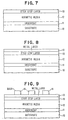
- FIG. 9 is analogous to FIG. 3, with the mask 14 formed on top of protective layer 13.
- FIG. 10 is analogous to FIG. 4 with the protective layer 13 being capable of being etched down to the etch stop layer 19 in grooves 17 without any danger of damage to the media layer 12 from the etching operation.
- FIG. 11 is analogous to FIG. 5 with the protective layer 13 exposed with the mask layer 14 removed.
- the encoded markings are separated by grooves 17.
- FIG. 12 is analogous to FIG. 6, with the optional uniformly oxidized surface layer 35, which is described in process step (7) above.
- the surface layer could be a material providing a protective layer such as a solid lubricant or a polymer.
- FIGS. 13-18 are analogous to FIGS. 1-6 with the exception that the magnetic media material 12 has been deposited upon the structure in the last step (FIG.18) with the capacitive pattern (26) formed below the magnetic media layer 12.
- a substrate 10 is show coated with an undercoat 11 as above.
- a dielectric layer 23 is deposited upon the undercoat 11.
- an ultra-thin (less than about 1,000 Angstroms thick) metallic layer 26 is deposited on dielectric layer 23. Then in a subsequent step, the metallic layer 26 has a patterned mask 14 formed on top of it.
- the metallic layer 26 has been formed into an ultra-thin pattern by etching to form coded pattern elements.
- the patterned metallic layer 26 is buried under an oxidized uniform surface layer 15, which in turn is coated with the magnetic media 12.
- the undercoat layer 11 is adapted to provide smoothing.
- Layer 23 is a nonmetallic dielectric layer.
- Layer 12, comprising the magnetic media can be metallic if thin enough to provide sufficient modulation in the surface of the disk to be detected. However, the surface roughness provided by the buried pattern elements 26 is slight enough to be almost undetectable with a profilometer.
- FIG. 19 shows another version of a buried metallic track 26 of FIGS. 7-12 (of coded pattern elements) under the magnetic media 12.
- Layers 12 and 26 are deposited upon a three layer structure comprising substrate 10, a metallic undercoat 11, and a dielectric layer 23.
- the relative thickness of magnetic media 12 to buried elements 26 is such that the surface roughness provided by buried elements 26 is almost undetectable by a profilometer, but still detectable by the capacitive servo sensor in the magnetic recording system.
- FIG. 20 is similar to FIG. 19 except that the thinness of the metallic magnetic media 22 on top of the disk is on the same order of magnitude as the ultra thin buried magnetic track 26 and since it is so thin, it has significant surface topography to be detected by the capacitive sensor in the magnetic recording system.
- a substrate 10 is coated with metallic undercoat 11, which is coated with dielectric layer 23, which in turn carries the metallic pattern elements 26 which provide servo patterns.
- the servo patterns 26 are coated with an ultra thin film of metallic magnetic media 22 (thinner than about 2000 Angstroms.)
- FIG. 21 is similar to FIG..6 or FIG. 12 except that planarization of the top surface is provided by a film of lubricant 27.
- Substrate 10 is coated with metallic undercoat 11 which is coated with magnetic layer 23 of CoCr.
- On top of layer 23 are chromium marking patterns 26 which are coated with lubricant 27.
- the lubricant 27 is planarized and thick enough to smooth over the encoded marking patterns 26.
- the lubricant 27 can be either viscous or solid.
- Suitable lubricant materials 27 include sputtered carbon, fluorocarbon layers, and materials such as those described in Linder et al, "ESCA Determination of Fluorocarbon Lubricant Film Thickness on Magnetic Disk Media" IEEE Transactions on Magnetics Vol.
- FIG. 22 shows a variation of the disk structure shown in FIG. 21, with the thick upper protection layer of chromium 26 being patterned in reverse with sputter-etched depressions 37, with no coating on top, with the very thin layer of chromium 26 not being planarized.
- a nonplanarized surface such as this provides better adhesion of a liquid lubricant, in that it reduces spin-off caused by inertial forces during rotation (centrifugal effect) and air shear forces.
- FIG. 23 shows a modification of FIG.22, with the substrate 10, metallic undercoat 11, magnetic layer 23, and a dielectric layer 36 of silicon dioxide, Si 3 N 4 , or sputtered carbon which is patterned by etched depressions 37, which can be only 200-400 Angstroms deep.
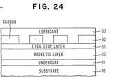
- FIG. 24 shows a modification of FIG.23, with the substrate 10, metallic undercoat 11, magnetic layer 23, and an etch stop layer 51 (composed of an etch stop material described above) covered by a pattern of coded indicia marked by sputtered carbon markings 52, which are covered by a lubricant layer 53 which planarizes the structure.
- the effective magnetic flying height is increased by the depth of modulation. That is, if 0.02 micrometers of additional patterned rhodium protective metal were added to the protective layer which is a continuous layer 700 Angstroms thick, the magnetic flying height is increased by perhaps 200 Angstroms , i.e. 0.02 micrometers. Smaller modulation depths can be sensed but are more prone to damage because of wear.
- Capacitive contrast caused by patterns buried beneath a protective layer are less susceptible to wear because the protective layer is worn, rather than the patterned layer and hence the capacitive signal will remain at the original contrast level.
- a 0.02 micrometer layer of Cr is deposited additively, using a lift-off technique on the Co Cr surface of the disk.
- the nonmagnetic thin layer of Cr, or nonmagnetic CoCr metallic film is sputter-etched or chemically-etched 0.02 or 0.03 micrometers deep into the metallic layer.
- the metallic pattern is overcoated by a thin lubrieant layer, and or by a thin dielectric layer of SiO 2 SiO 3 N 4 , A1 2 0 3 , Rh, and carbon, etc. or combinations thereof. When deposited by sputtering, this layer permits a small amount of levelling and decreases and protects the sharp edges of the metallic pattern.
- capacitive servo control data is stored on a metallic magnetic disk with minimal impact on the magnetic recording medium and the air bearing surfaces.
- the servo track is coated with a few hundred Angstroms of aluminum, to which resist is applied. Then the track pattern is exposed and developed. Next wet chemical etching is employed to etch the servo pattern in the aluminum. Alternatively if the aluminum is thin and the developing solution is strongly alkaline as in the case of a developer for azide type resist, it is possible to simultaneously develop the resist pattern and to etch the aluminum. Since the distension of the temporarily used pattern elements will be in the range of several hundred microns, wet etching will give acceptable results.
- Metallization can be deposited in an evaporator, but sputter deposition is preferable since the evaporation sources are prone to ejecting relatively large molten particles which would cause the formation of spikes or asperities on the disk surface which is clearly unacceptable.
- Aqueous or organic solution anodization of aluminum is useful for the purpose of forming planar structures in which case instead of removing the aluminum metal, aluminum is locally converted to aluminum oxide.
- a spinner was employed to apply photoresist to a 35,5 cm diameter disk with a special fixture adapted to minimize the risk of damage to the disk during processing.
- a vacuum frame was required to hold down the mask during exposure and a quartz halogen lamp was used for resist exposure.
- the etchant and the solvents used for wet chemical processing did not adversely affect the magnetic coating on the disk.
- the chemical used was an aqueous solution of KOH or NaOH.
- Aluminum pads about 50 micrometers by 15 micrometers in length and width and 600 Angstroms in thickness were fabricated by the lift-off process on 2,5 cm square coupons of AlMg disk coated with polyimide polymer or gamma-ferric oxide. Scanning electron micrographs show that the edges of the pads are more sharply defined by the lift-off process than by chemical etching.
- the surface of the Al pad on the magnetic material is rougher than that of polyimide, due to the roughness of the magnetic undercoating. This roughness however does not interfere with the level of capacitive signal or the S/N Ratio.
- Coupons of AlMg disk coated with polyimide or gamma ferric oxide were coated with 600 Angstroms of Al, which was then coated with resist.
- the coupons were then anodized in an 8% aqueous solution of oxalic acid until current ceased to flow.
- the resist was removed and the coupons were heated at 200 degrees C. to convert the anodic hydrated oxide to aluminum oxide.
Abstract
Description
- The present invention relates to data storage media and more particularly to patterning such media to provide servo control information on the media concurrently with maximum storage density and optimal accuracy of the servo system utilized to position the magnetic recording heads which read the data on the media.
- Heretofore, magnetic recording disk files have incorporated tracks for providing positioning information to a servo system which guides and controls the position of magnetic recording heads above the disk files as they search for the location where the data to be read is located. The servo system receives signals from a servo data sensor as it follows any selected one of a plurality of concentric magnetic recording tracks on the disk. Then the servo holds the head centered above such a selected recording track which contains data stored in the form of magnetic records on the disk files.
- Some magnetic disk files use a separate portion of the disk surface and a separate head (the servo head) on that surface for magnetically storing positioning information which provides the track location information followed by the servo system. In such files where there are a number of recording heads, all other recording heads are mechanically ganged to the servo head so that when the electronic servo system holds the servo head centered above a servo track, all other recording heads are approximately centered above their respective data tracks.
- Disadvantages of such dedicated magnetic servo tracks are, first, that each such track requires space on the magnetic disk, which precludes use of that space to store other data and secondly, that the track is "spaced away" from the data track. Thus, the mechanical alignment of the magnetic heads under servo control is less accurate than if the servo data were stored in alignment with the data track. Such "spacing away" introduces mechanical misalignments which yield errors in track following ability. This is a particular problem as economic trends dictate that magnetic disk files must have higher and higher track densities concomitantly with a requirement for higher performance servo systems.
- Another system of storing servo information on the magnetic disk is the "sector servo" system in which the servo information on the disk indicating track locations is stored in sectors of the disk file which are interspersed (i.e. inserted at spatial intervals along a circular track on the disk) around the surface of the disk. The servo information is stored between sectors in which data is stored.
- The advantage of the sector servo system is that the servo information is stored at the same track radius from the center of the disk as the data tracks containing the information to be read or which will contain the information to be stored by the head which is being controlled by the servo system. Thus since the track and the servo data are equal radial distances from the center of the disk, "spacing away" errors described above are eliminated.
- A disadvantage of the sector servo system is that like the concentric track system above, it uses up an area of. the magnetic disk surface for the storage of the servo control information which then cannot be used to store data. Thus it reduces the amount of space on the magnetic surface of the disk which can be employed to store data magnetically. A second disadvantage to the sector servo system is that mechanical vibrations at frequencies above one-half the rate at which the sectors pass the head are not controlled effectively by the servo system.
- Still another servo data storage system is the "buried servo" track in which the servo information is placed magnetically in the data disk, either in, below, or above the data containing layer - without reducing the data storage capacity of the data surface, usually by employing a recording medium other than a magnetic -me= dium to store the servo data.
- A number of such embedded servo systems have been proposed including magnetic, optical, and capacitive types. Capacitive servo techniques offer some advantages in implementation and detection, but embedded capacitive servo schemes are generally limited to dielectric magnetic media such as sputtered gamma Fe2 03because metallic magnetic films shield a capacitive sensor from a capacitive servo pattern lying beneath the magnetic layer. Because of increasing interest in media such as thin magnetic films for higher density horizontal as well as vertical recording, a new servo system is needed.
- Capacitive position signal schemes require a method of placing a pattern on a disk or tape which can be sensed capacitively. Such a scheme must be compatible with the magnetic media and must not affect flying or stop/start performance adversely.
- Copending U. S. patent application Ser. No. 06/494,743 filed May 16, 1983 of Krongelb, Romankiw, Scranton, and Thompson for a "Structure to Provide Optical and Capacitive Contrast on Magnetic Recording Disk" describes a method of placing a pattern with optical and capacitive contrast beneath a dielectric medium, such as a particulate medium or sputtered iron oxide. However that method is less advantageous with metallic conductive media which is both opaque to light and shields the capacitive sensor from the pattern capacitively.
- An alternate process is to remove the metallic medium in patterns in the form of dots, guard bands, a spiral or spirals, or other shapes so that the physical pattern of the medium itself can be sensed. Clearly, a problem with this is that magnetic data cannot be recorded on the portions of the disk where the medium has been removed, so the data recording density is reduced when this technique is employed.
- The invention as claimed is intended to remedy theabove mentioned drawbacks.
- The system of this invention provides a disk file with servo information stored by an extremely thin variable thickness layer providing a variable electromagnetic property such as variable capacitance which produces a contrast indicative of position. Signals in the form of changes in capacitive value are built into conductive metallic media for magnetic disks and tapes by a small amount of modulation of the thickness of the protective layer above the magnetic recording medium.
- Servo control systems for magnetic recording head drives require a method of placing a pattern on disk or tape units which can be sensed by means of a transducer such as a capacitive transducer. The pattern must be built into the units in a way which is compatible with the magnetic recording medium employed.
- Here the information to be detected by means of a capacitive sensor is recorded in the protective layer above the magnetic recording medium. For example, a thin film metallic protective layer 0.07 micrometers thick can be patterned with about 0.02 micrometers of the protective layer. -For a plated disk, the top 0.02 micrometers of the protective layer can be patterned.
- The pattern of the capacitive data can be formed subtractively by sputter etching, or additively formed by a lift-off process or by deposition through a mask. Alternatively, it can be done by anodization of a readily anodizable metal.
- In the worst case, the effective magnetic flying height can be increased very slightly.
- This system achieves capacitive contrast for markings indicative of the position on the disk or other medium providing signals on conductive metallic media for magnetic disks and tapes. The markings comprise very small amounts of modulation of the thickness of the protective layer above the magnetic recording medium.
- Alternatively, the capacitive contrast pattern can be stored in the protective layer above the magnetic media by a planar film. The planar film is composed of at least two materials with different dielectric constants or resistivities.
- A variety of electromagnetic sensors can be employed to detect the contrast patterns described below. Variations in height provide a phase contrast to an electromagnetic sensor, while variations in resistivity or dielectric constant provide changes in attenuation and impedance. The electromagnetic sensors include sensors adapted to detect eddy current infrared, optical and microwave electromagnetic energy, although a capacitive sensor is preferred in general because of the ease of incorporation of the sensing element-a thin metallic film in the construction of a magnetic read/write system.
- The foregoing and other objects, features and advantages of the invention, which is defined the attached claims, will be apparent from the more particular description of the preferred embodiments of the invention. as illustrated in the accompanying drawings, in which;
- FIG. 1 is a section of a magnetic recording disk to which a servo track is to be added as illustrated by FIGS. 2-6, in accordance with this invention.
- FIG.2 shows the disk of FIG. 1 after a protective layer has been added to the upper surface thereof.
- FIG. 3 shows the disk of FIG. 2 after it has been processed to add a temporary masking layer.
- FIG. 4 shows the disk of FIG. 3 after it has been processed by etching away some or all of the protective layer added in the process step associated with FIG. 2.
- FIG. 5 shows the disk after remaining masking material is removed, leaving the pattern etched in the protective layer during the process step associated with FIG. 4.
- FIG. 6 shows the result of adding of an oxidized uniform surface layer to the upper surface of the resulting structure of FIG. 5.
- FIG. 7 is a sectional view of the disk of FIG. 1 with the addition of an etch stop layer on top of the magnetic recording medium prior to addition of the servo track, as illustrated by FIGS. 8-12.
- FIG. 8 shows the disk of FIG. 7 after a protective layer has been added to the upper surface thereof.
- FIG. 9 shows the disk of FIG. 8 after it has been processed to add a temporary masking layer.
- FIG. 10 shows the disk 6f FIG. 9 after etching away some or all of the protective layer added in the process step associated with FIG. 8.
- FIG.11 shows the disk of FIG. 10 after remaining masking material is removed leaving the pattern etched in the protective layer.
- FIG. 12 shows the result of adding of an oxidized uniform surface layer to the upper surface of the resulting structure of FIG. 11.
- FIGS. 13-18 are analogous to FIGS. 1-6 where the magnetic media is applied to the upper surface of the structure at the end of the process rather than at the beginning.
- FIG. 19 is a modification of FIG. 18 with a buried metallic servo track with the magnetic media very thick with respect to the patterned metallic layer. Top surface height variations are detectable by capacitive sensors.
- FIG. 20 is a modification of FIG. 18, but as no oxidized uniform surface layer has been used. The height of the magnetic media is variable.
- FIG. 21 is similar to FIG. 6 or FIG. 12 except that the planarization of the top surface is provided by the disk lubricant.
- FIG. 22 shows a variation of the disk structure shown in FIG. 21, with a thick upper protection layer of chromium patterned in reverse with sputter-etched depressions with no coating on top.
- FIG. 23 shows a modification of FIG.22, with the substrate, metallic undercoat, magnetic layer, and a dielectric layer of silicon dioxide, Si3 N4, or sputtered carbon, patterned by very shallow etched depressions.
- FIG. 24 shows -a modification of FIG.23, with a layer of an etch stop material, covered by a pattern of coded indicia marked by sputtered carbon markings covered by a lubricant layer which planarizes the structure.
- In the drawings, like elements are designated with similar reference numbers, and identical elements in different specific embodiments are designated by identical reference numbers.
- A structure provides variable electromagnetic impedance (variable resistance, capacitive, or other variable electromagnetic or impedance value) contrast on the surface marking servo tracks on data storage medis. Such media include magnetic or optical storage disks and tapes. The media can be conductive metallic or nonmetallic and can be composed for example of poorly conductive media; dielectric media, or semiconductive media. The variable electromagnetic impedance can vary in the optical, electrical or other portions of the electromagnetic spectrum. A very small variation of the thickness of the protective layer above the magnetic recording medium is employed to mark the servo track information of the medium.
- Information to be detected by means of a capacitive sensor can be recorded in the protective layer above or below the magnetic re- cordin'g or optical storage medium. For example, a thin film metallic protective layer 0.07 micrometers thick can be patterned with about 0.02 micrometers of the protective layer. For a plated disk, the top 0.02 micrometers of the protective layer can be patterned.
- A pattern for providing a variable impedance for representing data can be formed subtractively by sputter etching, or additively formed by a lift-off process or by deposition through a mask, or by the oxidation of or nitriding of materials such as Al, Si or valve metals.
- This system provides a variable electromagnetic value such as variable capacitive reactance or other variable impedance contrast for position signals on conductive metallic media for magnetic disks and tapes by means of a very small amount of modulation of the thickness of the protective layer above the magnetic recording medium. Optionally, the protective layer may be planarized by subsequent oxidation, or the use of an additional layer.
- In accordance with this invention, a disk is formed by means of a series of additive and subtractive process steps. Further, the process may be improved such that the planarized combination of the protective layers and overcoat are formed from one deposition stop. Such a process is described below:
- 1) Deposit metallic magnetic medium on prepared substrate, as is well known in the state of the art listed as follows:
- a) K.Nakamura, Y.Ohta, A.Itoh, C. Hayashi, IEEE Trans. Mag., Vol 18, 1077-1079 (1982);
- T. Wielinga, J.C. Lodder, J. Worst, IEEE Trans Mag. Vol 18, 1107-1109(1982);
- Y. Suganuma, H. Tanaka, M. Yanagisawa, F. Goto, S. Hatano IEEE Trans. Mag. 'Vol. 18, 1215-1220 (1982).
- 2) Deposit a layer of Si, Cr, Al or of a valve metal;
- 3) Selectively mask predetermined portions of the layer of Si, Cr, Al or valve metal with photoresist with the photoresist having the desired capacitive servo pattern developed in it. The photoresist can be an X-ray or electron beam sensitive material as well.
- 4) Partially etch the layer of Si, Cr, Al, Rh, Ir, Os, or valve metal through the openings in the mask.
- One could stop at this point. The patterned surface topography provides a capacitive signal for position measurement. Correspondingly, the surface provides an optically sensed signal through phase contrast.
- 5) Oxidize the layer of Si, Cr, Al or valve metal through the openings in the mask. Oxidation may be aqueous, or organic anodic electrochemical, thermal or oxygen plasma assisted. The proper depth of partial etching, in combination with the increase in film thickness due to oxidation, will planarize the surface.
- One could perform step (5) immediately after step (3). However, in that case, one would not achieve planarization.
- 6) The masking material is removed (optional) by means of an appropriate solvent for the resist used in the operation (acetone when using azide (AZ) type resist, and an appropriate solvent when using PMA or other resists.)
- 7) The entire surface may be uniformly oxidized to provide an (optional) uniform surface. Capacitive contrast is achieved by the variations in resistivity and dielectric constant in different regions which occur through the patterned selective etching and oxidation process. The pattern may be detected optically as the material properties of resistivity and dielectric constant in the optical range are more commonly known as optical absorption and index of refraction.
- The following description relates to an implementation of the seven process steps listed above. A magnetic recording-
disk 9 of the conventional sort is shown in FIG. 1, ready for processing of a servo track ontodisk 9 in accordance with this invention. Thesubstrate 10 which is composed of AlMg alloy is coated with anundercoat layer 11 composed of an NiP alloy. The undercoat supports the magneticrecording medium layer 12 composed of CoCr, CoPt, CoP, or CoNiP, which is applied in accordance with process step (1) above. - In FIG. 2, the
disk 9 of FIG. 1 is coated with aprotective layer 13 is deposited ontomagnetic media layer 12 ofdisk 9, in accordance with process step (2) above.Layer 13 is composed of one of several materials (such as Si, Al or a valve metal) selected from the group consisting of Ni, V, Ta, Ti, Zr, Hf, Cr, Mo, W, Mg, Si, Al, Rh, Ir, Os, or alloys thereof. This layer protectsmagnetic media layer 12 from corrosion and wear. This is important because the magnetic film is extremely thin and would be strongly affected by loss of material to corrosion and wear. Also, a magnetic recording head reads and writes data when it is in close proximity to the media and the surface of the head would be deleteriously affected by wear products. Theprotective layer 13 allows alternate choices for protection from wear and corrosion than the limited materials available forlayer 12, which are chosen for magnetic properties. - FIG. 3 shows the
disk 9 of FIG. 2 with amask layer 14 composed of a resist such as photoresist, x-ray resist, or electron beam resist which is patterned in accordance with the pattern of the ultimate capacitive structure to be etched into thedisk 9, in accordance with step (3) above. Themask layer 14 is applied selectively to provide the desired capacitive pattern to be formed by etching of theprotective layer 14. The photoresist is composed of AZ Shipley resist or PMMA, preferably.Mask 14 includes grooves oropenings 17 through whichprotective layer 13 is partially etched in step (4) above. - FIG. 4 shows the
disk 9 of FIG. 3 after theprotective layer 13 has been partially etched from above along the z axis down into thelayer 13 by etching through theopenings 17 in themask 14, as described in process step (4) above. - Next in process step (5) the surfaces of
layer 13 which are not protected by mask 14 (i.e. in grooves oropenings 17 in mask 14) are exposed to oxidization by an atmosphere of oxygen plasma, by aqueous solution or by an organic anodization solution. - The oxidation results in oxidized
layer 40 which increases the volume at the exposedopenings 17 oflayer 13, as it converts metal inlayer 13 to a metal oxide as this process increases the distance between the metal atoms by inserting oxygen atoms in between metal atoms. - As an alternative in this step, one can oxidize partially. While it is possible to use the magnetic disk file as produced thus far, it is preferable to process it further as shown in connection with FIG. 5 for better performance characteristics.
- FIG. 5 shows the
disk 9 of FIG. 4 after the resistmask 14 has been removed from theprotective layer 13 as in process step (6) above, exposing the encodedmarkings 16 formed by the remaining portions ofprotective layer 13, which along with thegrooves 17 betweenmarkings 16 provide variations in dielectric constant with dimensions along the z axis on the order of 0.02 micrometers. Oxidation provides better protection and may produce a smoother surface. - FIG. 6 shows the
disk 9 of FIG.5 afterdisk 9 has been treated by further oxidizing of the material of the protective layer 13 (with oxidation occurring throughlayer 40 where it exists) to form an oxidized, uniform-surface layer 15, as described in process step (7) above. This is done because the oxidizedlayer 15 provides the actual wear surface of thelayer 13.Layer 40 andlayer 15 are composed of the same material, but the thickness of thelayer 40 plus thelayer 15 is greater than the thickness oflayer 15, wherelayer 40 is absent.Layer 40 is formed only in the openings inmask 14. - Alternatively, to the process of steps 1-6, the process can be performed in much the same way with the difference that the etching step is controlled by a stop layer.
- During the selective etching or oxidation of the patterned layer, it is highly desirable that the magnetic media should not be etched. Etching or oxidation of the magnetic media may lead to variation in the magnetic recording properties of the media. In effect, the capacitive contrast pattern may be sensed magnetically, with deleterious effects on the magnetic read-write system. Although such a system may still function, it is preferable that the magnetic layer should neither be etched nor oxidized to produce a capacitive servo pattern thereon.
- For this reason, either care is taken to assure that the
protective layer 13 of Si, a metal such as Al, or a valve metal is not fully etched or an additional layer, called the "stop layer" is deposited prior to theprotective layer 13. The purpose of the "stop" layer (see FIGS. 8-12 and 24) is to prevent etching or oxidation of the magnetic media. - A second reason for the stop layer is to reduce the generation of defects in the
magnetic media layer 12 from defects inprotective layer 13. All deposition processes produce some defects. These defects are to be minimized. Defects which have the nature of missing material (pinholes), for example, missing small portions ofprotective layer 13, may cause defects in the magnetic media upon subsequent etching or oxidation. The application of the two separate layers,protective layer 13 and the etch-stop layer 19 in FIGS. 7-12 reduces such process-caused, magnetic defects because only defects which occur in both theprotective layer 13 and thestop layer 19 at the same location will cause magnetic defects upon etching and oxidation. To the extent that the missing material defects are uncorrelated from layer to layer, the existence of missing material defects in both layers (protective layer 13 and stop layer 19) at the same location is statistically very unlikely. In this case theprotective layer 13 can be composed of materials such as Si, Cr, Al or a valve metal, as shown in FIGS. 7-12.Substrate 10,undercoat 11 and magnetic media can be the same as in FIGS. 1-6. - For example perfluorinated hydrocarbons, silicon dioxide, silicon nitride and aluminum oxide or inorganic or organic glasses can be used as "stop"
layer 19 for pattern oxidation of a pattern layer of a material selected from the group of materials consisting of Hg, Nb, Ta, and Cr Si, when used withmagnetic media 12 composed of a material selected from CrCo, CoP and CoNiP. - If due to process variation and tolerances, the pattern layer is fully oxidized before the oxidation process step is over, the
stop layer 19 will prevent oxidation of themagnetic media 12. - In fact the subsequent final oxidized
uniform protection layer 35 in FIG.12 may totally planarize the disk surface. Variation in the electrical impedance due to changes in the relative thickness of the overcoat and protective layers will still provide a capacitive contrast for a servo position signal. - As shown in FIG. 7 which is similar to FIG. 1 in terms of the
substrate 10,undercoat layer 11 andmagnetic media layer 12. - Themedia layer 12 is also coated in process step 1 with anetch stop layer 19 which will prevent the subsequent etching step from reaching down to themedia 12 so that the media will be protected from formation of any modifications which would tend to cause false or erroneous readings. Theetch stop layer 19 is composed of a material such as those described above. - FIG. 8 which is analogous to FIG. 2, shows the device of FIG.7 after the
protective layer 13 composed of a material such as Si, a metal such as Cr or Al or a valve metal, has been deposited upon theetch stop layer 19. - FIG. 9 is analogous to FIG. 3, with the
mask 14 formed on top ofprotective layer 13. - FIG. 10 is analogous to FIG. 4 with the
protective layer 13 being capable of being etched down to theetch stop layer 19 ingrooves 17 without any danger of damage to themedia layer 12 from the etching operation. - FIG. 11 is analogous to FIG. 5 with the
protective layer 13 exposed with themask layer 14 removed. The encoded markings are separated bygrooves 17. - FIG. 12 is analogous to FIG. 6, with the optional uniformly oxidized
surface layer 35, which is described in process step (7) above. The surface layer could be a material providing a protective layer such as a solid lubricant or a polymer. One could also deposit an oxide or form an oxidizedlayer 35. - FIGS. 13-18 are analogous to FIGS. 1-6 with the exception that the
magnetic media material 12 has been deposited upon the structure in the last step (FIG.18) with the capacitive pattern (26) formed below themagnetic media layer 12. - In FIG. 13, a
substrate 10 is show coated with anundercoat 11 as above. - In FIG. 14, a
dielectric layer 23 is deposited upon theundercoat 11. - In FIG. 15, an ultra-thin (less than about 1,000 Angstroms thick)
metallic layer 26 is deposited ondielectric layer 23. Then in a subsequent step, themetallic layer 26 has a patternedmask 14 formed on top of it. - In FIG. 16, the
metallic layer 26 has been formed into an ultra-thin pattern by etching to form coded pattern elements. - In FIG. 17, the
mask 14 is removed, leaving the coded pattern elements ofmetallic layer 26 exposed completely. - In FIG. 18, the patterned
metallic layer 26 is buried under an oxidizeduniform surface layer 15, which in turn is coated with themagnetic media 12. - Referring in particular to FIG. 18, -the
undercoat layer 11 is adapted to provide smoothing.Layer 23 is a nonmetallic dielectric layer.Layer 12, comprising the magnetic media can be metallic if thin enough to provide sufficient modulation in the surface of the disk to be detected. However, the surface roughness provided by the buriedpattern elements 26 is slight enough to be almost undetectable with a profilometer. - FIG. 19 shows another version of a buried
metallic track 26 of FIGS. 7-12 (of coded pattern elements) under themagnetic media 12.Layers structure comprising substrate 10, ametallic undercoat 11, and adielectric layer 23. The relative thickness ofmagnetic media 12 to buriedelements 26 is such that the surface roughness provided by buriedelements 26 is almost undetectable by a profilometer, but still detectable by the capacitive servo sensor in the magnetic recording system. - FIG. 20 is similar to FIG. 19 except that the thinness of the metallic
magnetic media 22 on top of the disk is on the same order of magnitude as the ultra thin buriedmagnetic track 26 and since it is so thin, it has significant surface topography to be detected by the capacitive sensor in the magnetic recording system. Asubstrate 10 is coated withmetallic undercoat 11, which is coated withdielectric layer 23, which in turn carries themetallic pattern elements 26 which provide servo patterns. Theservo patterns 26 are coated with an ultra thin film of metallic magnetic media 22 (thinner than about 2000 Angstroms.) - FIG. 21 is similar to FIG..6 or FIG. 12 except that planarization of the top surface is provided by a film of
lubricant 27.Substrate 10 is coated withmetallic undercoat 11 which is coated withmagnetic layer 23 of CoCr. On top oflayer 23 arechromium marking patterns 26 which are coated withlubricant 27. Thelubricant 27 is planarized and thick enough to smooth over the encoded markingpatterns 26. Thelubricant 27 can be either viscous or solid.Suitable lubricant materials 27 include sputtered carbon, fluorocarbon layers, and materials such as those described in Linder et al, "ESCA Determination of Fluorocarbon Lubricant Film Thickness on Magnetic Disk Media" IEEE Transactions on Magnetics Vol. MAG-18, No. 6, 1073-1076, (Nov. 1982); and V. Au-Yeung "FTIR Determination of Fluorocarbon Lubricant Film Thickness on Magnetic Disk Media", IEEE Transactions on Magnetics, Vol. MAG-19, No.5, 1662-1664) (Sep.1983). - FIG. 22 shows a variation of the disk structure shown in FIG. 21, with the thick upper protection layer of
chromium 26 being patterned in reverse with sputter-etcheddepressions 37, with no coating on top, with the very thin layer ofchromium 26 not being planarized. A nonplanarized surface such as this provides better adhesion of a liquid lubricant, in that it reduces spin-off caused by inertial forces during rotation (centrifugal effect) and air shear forces. - FIG. 23 shows a modification of FIG.22, with the
substrate 10,metallic undercoat 11,magnetic layer 23, and adielectric layer 36 of silicon dioxide, Si3N4, or sputtered carbon which is patterned by etcheddepressions 37, which can be only 200-400 Angstroms deep. - FIG. 24 shows a modification of FIG.23, with the
substrate 10,metallic undercoat 11,magnetic layer 23, and an etch stop layer 51 (composed of an etch stop material described above) covered by a pattern of coded indicia marked by sputteredcarbon markings 52, which are covered by alubricant layer 53 which planarizes the structure. - In the worst case, the effective magnetic flying height is increased by the depth of modulation. That is, if 0.02 micrometers of additional patterned rhodium protective metal were added to the protective layer which is a continuous layer 700 Angstroms thick, the magnetic flying height is increased by perhaps 200 Angstroms , i.e. 0.02 micrometers. Smaller modulation depths can be sensed but are more prone to damage because of wear.
- Capacitive contrast caused by patterns buried beneath a protective layer are less susceptible to wear because the protective layer is worn, rather than the patterned layer and hence the capacitive signal will remain at the original contrast level.
- We have detected capacitive signals from a 0.025 micrometers thick metallic servo pattern formed on a 0.5 micrometer thick dielectric particulate magnetic medium with a relative permitivity or dielectric constant (epsilon greater than 10) for the dielectric particulate medium with a 42 db Signal-to-Noise (S/N) ratio.
- Also, we have detected capacitive signals from a 0.025 micrometer aluminum pattern that was deposited by evaporation onto a CoCr magnetic medium on an NiP underlayer on an AlMg disk. The detected S/N ratio was 46 db.
- In the case of a CoCr disk, a 0.02 micrometer layer of Cr is deposited additively, using a lift-off technique on the Co Cr surface of the disk. Alternatively, the nonmagnetic thin layer of Cr, or nonmagnetic CoCr metallic film is sputter-etched or chemically-etched 0.02 or 0.03 micrometers deep into the metallic layer. To protect the metallic pattern from wear, the metallic pattern is overcoated by a thin lubrieant layer, and or by a thin dielectric layer of SiO2 SiO3N4, A1203, Rh, and carbon, etc. or combinations thereof. When deposited by sputtering, this layer permits a small amount of levelling and decreases and protects the sharp edges of the metallic pattern. In summary, capacitive servo control data is stored on a metallic magnetic disk with minimal impact on the magnetic recording medium and the air bearing surfaces.
- Several potential processes have been identified for fabrication of capacitive servo tracks with 200 to about 1000 Angstroms thick aluminum.
- They include
- 1. Chemical etching (acceptable only for very thin films and large geometry with a suitably selective chemical etchant which does not attack the layer underneath chemically;)
- 2. Lift-off (acceptable for small geometry but with lithography being more demanding;)
- 3. Dry anodization and plasma-assisted anodization; and
- 4. Wet anodization.
- The servo track is coated with a few hundred Angstroms of aluminum, to which resist is applied. Then the track pattern is exposed and developed. Next wet chemical etching is employed to etch the servo pattern in the aluminum. Alternatively if the aluminum is thin and the developing solution is strongly alkaline as in the case of a developer for azide type resist, it is possible to simultaneously develop the resist pattern and to etch the aluminum. Since the distension of the temporarily used pattern elements will be in the range of several hundred microns, wet etching will give acceptable results.
- Metallization can be deposited in an evaporator, but sputter deposition is preferable since the evaporation sources are prone to ejecting relatively large molten particles which would cause the formation of spikes or asperities on the disk surface which is clearly unacceptable.
- Aqueous or organic solution anodization of aluminum is useful for the purpose of forming planar structures in which case instead of removing the aluminum metal, aluminum is locally converted to aluminum oxide.
- A spinner was employed to apply photoresist to a 35,5 cm diameter disk with a special fixture adapted to minimize the risk of damage to the disk during processing. A vacuum frame was required to hold down the mask during exposure and a quartz halogen lamp was used for resist exposure. The etchant and the solvents used for wet chemical processing did not adversely affect the magnetic coating on the disk. The chemical used was an aqueous solution of KOH or NaOH.
- Aluminum pads about 50 micrometers by 15 micrometers in length and width and 600 Angstroms in thickness were fabricated by the lift-off process on 2,5 cm square coupons of AlMg disk coated with polyimide polymer or gamma-ferric oxide. Scanning electron micrographs show that the edges of the pads are more sharply defined by the lift-off process than by chemical etching. The surface of the Al pad on the magnetic material is rougher than that of polyimide, due to the roughness of the magnetic undercoating. This roughness however does not interfere with the level of capacitive signal or the S/N Ratio.
- Coupons of AlMg disk coated with polyimide or gamma ferric oxide were coated with 600 Angstroms of Al, which was then coated with resist. The coupons were then anodized in an 8% aqueous solution of oxalic acid until current ceased to flow. The resist was removed and the coupons were heated at 200 degrees C. to convert the anodic hydrated oxide to aluminum oxide.
Claims (26)
Applications Claiming Priority (2)
| Application Number | Priority Date | Filing Date | Title |
|---|---|---|---|
| US61394384A | 1984-05-24 | 1984-05-24 | |
| US613943 | 1984-05-24 |
Publications (2)
| Publication Number | Publication Date |
|---|---|
| EP0162349A2 true EP0162349A2 (en) | 1985-11-27 |
| EP0162349A3 EP0162349A3 (en) | 1988-09-07 |
Family
ID=24459300
Family Applications (1)
| Application Number | Title | Priority Date | Filing Date |
|---|---|---|---|
| EP85105240A Withdrawn EP0162349A3 (en) | 1984-05-24 | 1985-04-30 | A data recording medium |
Country Status (3)
| Country | Link |
|---|---|
| EP (1) | EP0162349A3 (en) |
| JP (1) | JPS60261083A (en) |
| CA (1) | CA1241741A (en) |
Cited By (10)
| Publication number | Priority date | Publication date | Assignee | Title |
|---|---|---|---|---|
| EP0166614A2 (en) * | 1984-06-29 | 1986-01-02 | Minnesota Mining And Manufacturing Company | Encoated optical recording medium |
| GB2196467A (en) * | 1986-10-11 | 1988-04-27 | London Weekend Television | Optical disc with added magnetic record/playback facility |
| US4931887A (en) * | 1988-02-01 | 1990-06-05 | International Business Machines Corporation | Capacitive measurement and control of the fly height of a recording slider |
| EP0450629A1 (en) * | 1990-04-06 | 1991-10-09 | Sony Corporation | Recording and reproducing device and recording medium therefor |
| WO1992018977A1 (en) * | 1991-04-23 | 1992-10-29 | Gec Avery Limited | Magnetic data medium and its production, data system and data decoding device |
| EP1318513A2 (en) * | 2001-12-06 | 2003-06-11 | Samsung Electronics Co., Ltd. | Information storage apparatus using charge |
| WO2004032116A1 (en) * | 2002-10-03 | 2004-04-15 | Koninklijke Philips Electronics N.V. | Read only storage system |
| EP1538608A2 (en) * | 2003-10-20 | 2005-06-08 | Quantum Corporation | Electromagnetic void-sensing probes and position control systems |
| US7378028B2 (en) * | 2004-06-03 | 2008-05-27 | Seagate Technology Llc | Method for fabricating patterned magnetic recording media |
| US7649707B2 (en) | 2005-03-18 | 2010-01-19 | Quantum Corporation | Auto-servo tape system and associated recording head |
Families Citing this family (1)
| Publication number | Priority date | Publication date | Assignee | Title |
|---|---|---|---|---|
| US4684547A (en) * | 1985-12-27 | 1987-08-04 | International Business Machines Corporation | Format patterning method for magnetic recording media |
Citations (6)
| Publication number | Priority date | Publication date | Assignee | Title |
|---|---|---|---|---|
| GB2046480A (en) * | 1979-03-27 | 1980-11-12 | Tokyo Shibaura Electric Co | Tracking servo and playback system for video disc |
| GB2056721A (en) * | 1979-07-09 | 1981-03-18 | Rca Corp | Stylus position sensing apparatus for a disc record player |
| GB2084786A (en) * | 1980-09-25 | 1982-04-15 | Rca Corp | Variable sensitivity optical recording medium and information record |
| EP0061584A1 (en) * | 1981-03-24 | 1982-10-06 | Kabushiki Kaisha Toshiba | Pregrooved optical-disk |
| EP0125478A2 (en) * | 1983-05-16 | 1984-11-21 | International Business Machines Corporation | Magnetic record disk with internal servo track |
| EP0130329A1 (en) * | 1983-06-02 | 1985-01-09 | International Business Machines Corporation | Optical data storage medium |
-
1985
- 1985-03-28 CA CA000477749A patent/CA1241741A/en not_active Expired
- 1985-04-10 JP JP60074553A patent/JPS60261083A/en active Pending
- 1985-04-30 EP EP85105240A patent/EP0162349A3/en not_active Withdrawn
Patent Citations (6)
| Publication number | Priority date | Publication date | Assignee | Title |
|---|---|---|---|---|
| GB2046480A (en) * | 1979-03-27 | 1980-11-12 | Tokyo Shibaura Electric Co | Tracking servo and playback system for video disc |
| GB2056721A (en) * | 1979-07-09 | 1981-03-18 | Rca Corp | Stylus position sensing apparatus for a disc record player |
| GB2084786A (en) * | 1980-09-25 | 1982-04-15 | Rca Corp | Variable sensitivity optical recording medium and information record |
| EP0061584A1 (en) * | 1981-03-24 | 1982-10-06 | Kabushiki Kaisha Toshiba | Pregrooved optical-disk |
| EP0125478A2 (en) * | 1983-05-16 | 1984-11-21 | International Business Machines Corporation | Magnetic record disk with internal servo track |
| EP0130329A1 (en) * | 1983-06-02 | 1985-01-09 | International Business Machines Corporation | Optical data storage medium |
Non-Patent Citations (3)
| Title |
|---|
| IBM TECHNICAL DISCLOSURE BULLETIN, vol. 17, no. 11, April 1975, page 3306, New York, US; A. STOFFEL "Pattern consisting of a magnetic material and method of producing the pattern" * |
| IBM TECHNICAL DISCLOSURE BULLETIN, vol. 25, no. 11A, April 1983, pages 5442-5443; M.R. LORENZ "Buried servo-data layer structure for magnetic recording" * |
| IBM TECHNICAL DISLOSURE BULLETIN, vol. 23, no. 7A, December 1980, pages 2949-2950; T.N. KENNEDY "Magnetic recording disk with buried servo layer" * |
Cited By (14)
| Publication number | Priority date | Publication date | Assignee | Title |
|---|---|---|---|---|
| EP0166614A2 (en) * | 1984-06-29 | 1986-01-02 | Minnesota Mining And Manufacturing Company | Encoated optical recording medium |
| EP0166614A3 (en) * | 1984-06-29 | 1987-12-23 | Minnesota Mining And Manufacturing Company | Encoated optical recording medium |
| GB2196467A (en) * | 1986-10-11 | 1988-04-27 | London Weekend Television | Optical disc with added magnetic record/playback facility |
| US4931887A (en) * | 1988-02-01 | 1990-06-05 | International Business Machines Corporation | Capacitive measurement and control of the fly height of a recording slider |
| US5488519A (en) * | 1990-04-06 | 1996-01-30 | Sony Corporation | Recording and reproducing device having conductive spindle |
| EP0450629A1 (en) * | 1990-04-06 | 1991-10-09 | Sony Corporation | Recording and reproducing device and recording medium therefor |
| WO1992018977A1 (en) * | 1991-04-23 | 1992-10-29 | Gec Avery Limited | Magnetic data medium and its production, data system and data decoding device |
| EP1318513A2 (en) * | 2001-12-06 | 2003-06-11 | Samsung Electronics Co., Ltd. | Information storage apparatus using charge |
| EP1318513A3 (en) * | 2001-12-06 | 2005-12-28 | Samsung Electronics Co., Ltd. | Information storage apparatus using charge |
| WO2004032116A1 (en) * | 2002-10-03 | 2004-04-15 | Koninklijke Philips Electronics N.V. | Read only storage system |
| EP1538608A2 (en) * | 2003-10-20 | 2005-06-08 | Quantum Corporation | Electromagnetic void-sensing probes and position control systems |
| EP1538608A3 (en) * | 2003-10-20 | 2007-12-19 | Quantum Corporation | Electromagnetic void-sensing probes and position control systems |
| US7378028B2 (en) * | 2004-06-03 | 2008-05-27 | Seagate Technology Llc | Method for fabricating patterned magnetic recording media |
| US7649707B2 (en) | 2005-03-18 | 2010-01-19 | Quantum Corporation | Auto-servo tape system and associated recording head |
Also Published As
| Publication number | Publication date |
|---|---|
| CA1241741A (en) | 1988-09-06 |
| JPS60261083A (en) | 1985-12-24 |
| EP0162349A3 (en) | 1988-09-07 |
Similar Documents
| Publication | Publication Date | Title |
|---|---|---|
| US4737877A (en) | Structure to provide optical and capacitive contrast on magnetic recording disk | |
| US6586044B1 (en) | Method for manufacturing a magnetic hard disk having concentric magnetic tracks with flat surface | |
| US5504646A (en) | Magnetic disk including protective layer having surface with protusions and magnetic disk apparatus including the magnetic disk | |
| US5159508A (en) | Magnetic head slider having a protective coating thereon | |
| EP0339813B1 (en) | A discrete track thin film magnetic record disk and a method of making it | |
| US5175658A (en) | Thin film magnetic head having a protective coating and method for making same | |
| US5271802A (en) | Method for making a thin film magnetic head having a protective coating | |
| EP0452876A2 (en) | A longitudinal magnetic recording medium | |
| US20030022024A1 (en) | Aluminum substrate disk having silica gel coating | |
| US5986851A (en) | Selective carbon overcoat of the trailing edge of MR sliders | |
| EP0162349A2 (en) | A data recording medium | |
| US5241440A (en) | Thin film magnetic head and manufacturing method therefor | |
| US6051299A (en) | Magnetic recording medium, magnetic recording/reproducing apparatus and method for manufacturing metallic mold for molding disc | |
| US6614608B1 (en) | Buried servo patterned media | |
| US7746598B2 (en) | Information recording medium and recording/reproducing apparatus | |
| EP0464786B1 (en) | Magnetic disk, method of manufacturing the same and magnetic disk apparatus including the magnetic disk | |
| US6477011B1 (en) | Magnetic recording device having an improved slider | |
| EP0477031B1 (en) | Magnetic storage system and manufacturing method for a magnetic storage medium thereof | |
| EP0493902B1 (en) | Magnetic head slider and method for making same | |
| EP0125478B1 (en) | Magnetic record disk with internal servo track | |
| JPH04141822A (en) | Magnetic disk and magnetic disk device | |
| JP2539536B2 (en) | Thin film magnetic head and manufacturing method thereof | |
| US20110038082A1 (en) | Combined cmp and etch planarization | |
| JPH0489616A (en) | Magnetic disk device and magnetic disk | |
| JPH02189715A (en) | Magnetic disk and production thereof and recorder |
Legal Events
| Date | Code | Title | Description |
|---|---|---|---|
| PUAI | Public reference made under article 153(3) epc to a published international application that has entered the european phase |
Free format text: ORIGINAL CODE: 0009012 |
|
| AK | Designated contracting states |
Designated state(s): DE FR GB IT |
|
| 17P | Request for examination filed |
Effective date: 19860325 |
|
| PUAL | Search report despatched |
Free format text: ORIGINAL CODE: 0009013 |
|
| AK | Designated contracting states |
Kind code of ref document: A3 Designated state(s): DE FR GB IT |
|
| 17Q | First examination report despatched |
Effective date: 19890804 |
|
| STAA | Information on the status of an ep patent application or granted ep patent |
Free format text: STATUS: THE APPLICATION IS DEEMED TO BE WITHDRAWN |
|
| 18D | Application deemed to be withdrawn |
Effective date: 19900529 |
|
| RIN1 | Information on inventor provided before grant (corrected) |
Inventor name: THOMPSON, DAVID ALLEN Inventor name: ROMANKIW, LUBOMYR TARAS Inventor name: BEST, JOHN STEWARD Inventor name: SCRANTON, ROBERT ALAN |