EP0385867A2 - Digital signal reproducing apparatus - Google Patents
Digital signal reproducing apparatus Download PDFInfo
- Publication number
- EP0385867A2 EP0385867A2 EP90400566A EP90400566A EP0385867A2 EP 0385867 A2 EP0385867 A2 EP 0385867A2 EP 90400566 A EP90400566 A EP 90400566A EP 90400566 A EP90400566 A EP 90400566A EP 0385867 A2 EP0385867 A2 EP 0385867A2
- Authority
- EP
- European Patent Office
- Prior art keywords
- signal
- data
- output
- comparator
- circuit
- Prior art date
- Legal status (The legal status is an assumption and is not a legal conclusion. Google has not performed a legal analysis and makes no representation as to the accuracy of the status listed.)
- Granted
Links
Images


Classifications
-
- H—ELECTRICITY
- H04—ELECTRIC COMMUNICATION TECHNIQUE
- H04N—PICTORIAL COMMUNICATION, e.g. TELEVISION
- H04N5/00—Details of television systems
- H04N5/76—Television signal recording
- H04N5/91—Television signal processing therefor
- H04N5/93—Regeneration of the television signal or of selected parts thereof
- H04N5/931—Regeneration of the television signal or of selected parts thereof for restoring the level of the reproduced signal
-
- G—PHYSICS
- G11—INFORMATION STORAGE
- G11B—INFORMATION STORAGE BASED ON RELATIVE MOVEMENT BETWEEN RECORD CARRIER AND TRANSDUCER
- G11B20/00—Signal processing not specific to the method of recording or reproducing; Circuits therefor
- G11B20/10—Digital recording or reproducing
- G11B20/10009—Improvement or modification of read or write signals
-
- G—PHYSICS
- G11—INFORMATION STORAGE
- G11B—INFORMATION STORAGE BASED ON RELATIVE MOVEMENT BETWEEN RECORD CARRIER AND TRANSDUCER
- G11B20/00—Signal processing not specific to the method of recording or reproducing; Circuits therefor
- G11B20/10—Digital recording or reproducing
- G11B20/10527—Audio or video recording; Data buffering arrangements
-
- H—ELECTRICITY
- H04—ELECTRIC COMMUNICATION TECHNIQUE
- H04N—PICTORIAL COMMUNICATION, e.g. TELEVISION
- H04N5/00—Details of television systems
- H04N5/76—Television signal recording
- H04N5/91—Television signal processing therefor
- H04N5/92—Transformation of the television signal for recording, e.g. modulation, frequency changing; Inverse transformation for playback
- H04N5/926—Transformation of the television signal for recording, e.g. modulation, frequency changing; Inverse transformation for playback by pulse code modulation
Definitions
- the present invention relates generally to a device for reproducing magnetically recorded data and more specifically is directed to an apparatus for reproducing video signals which have been digitized.
- the video signal is frequency modulated and then recorded as an analog signal on magnetic tape.
- the video signal is converted into a digital signal prior to recording, it is possible to repeatedly dub or copy the recorded signals without incurring any deterioration in the characteristics thereof.
- the magnetic head, the tape and the like of the electromagnetic transducing system exhibit characteristics which, in the low frequency and high frequency regions, cause reduction in the S/N ratio.
- a digitized video signal (hereinafter referred to as a digital signal) may be limited to a narrow frequency range. Therefore, it is necessary to use a recording system by which the frequency spectrum enables the S/N ratio to approach its maximum value.
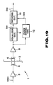
- a video recorder which ahs been proposed in order to take advantage of the fact that digital video signals can be dubbed without undergoing any deterioration, is shown on Fig. 19.
- predetermined recording data D REC is supplied via an amplifier 3 to a magnetic recording head 4 and recorded thereby on magnetic tape 5.
- a magnetic playback head 6 is used to reproduce a signal S RF which is supplied through an amplifier 8 and an equalizing circuit 9 to a decoding circuit 10.
- a clock signal Sck is produced by a clock signal generator 12 and supplied to the decoding circuit 10.
- the decoding circuit 10 responds thereto by checking the level of the reproduced signal S RF with respect to a predetermined reference value, at a predetermined timing, and outputting reproduction characteristic data D RB which is then used to decode the digitized video signal.
- a slice level value in the decoding circuit 10 may become variable and it then becomes necessary to prevent bit error from appearing in the reproduction characteristic data.
- an arrangement having a Viterbi decoding circuit in which, when data falls within a predetermined range, the level of the reproduced signal is sensed and the level of the reproduced signal is corrected in a manner which reduces bit error caused by noise in the reproduced signal.
- a device for reproducing magnetic recordings features means for recording data on a recording media and for obtaining a reproduced signal therefrom and means for correcting a previous input data value in response to change in an instant input data value.
- a system for recording and reproducing data comprises means for converting an input signal from analog form into digital data; a moving body on which the digital data can be recorded; means for reading the data recorded on the moving body and producing an analog playback signal indicative thereof; means for converting the analog playback signal into a digital playback signal; signal dividing means for separating the digital playback signal into first and second signal portions; first and second Viterbi decoding circuits which respectively receive the first and second signal portions; signal re-combining means for receiving the outputs of the first and second Viterbi decoding circuits and forming a reconstituted digital signal; means for converting the reconstituted digital into an analog output signal; and means associated with the first and second Viterbi decoding circuits for modifying either the output of, or the signal which is input to the first and second viterbi circuits to reduce the bit error in the output of the first and second Viterbi circuits.
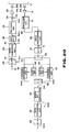
- a recording and/or reproducing device 20 comprises a recording section having an A/D converter 22, a data compression circuit 24, an error correction circuit 26, a pre-coding circuit 28, an adder 29, an amplifier 30 and recording heads 4A and 4B which are serially connected.
- the device 20 further comprises a playback section which includes an amplifier 8, an equalizer circuit 9, a variable gain amplifier 31, a calculation processing circuit 32 and an A/D converter 37 which are also serially connected.
- a first selection or switching circuit 39 is connected to the output of the A/D converter 37 and is arranged to selectively switch between first and second Viterbi decoding circuits 40 and 41.
- the outputs of the Viterbi circuits 40 and 41 are connected with a second selection or switching circuit 80 which selectively channels data from the Viterbi circuits 40 and 41 to a series circuit of an error detection and correction circuit 81, a data expansion circuit 82 and a D/A converter 83.
- a comparator 70 has one of its three inputs connected to terminals of the Viterbi circuits 40 and 41 from which data ⁇ K are output. The other two inputs of the comparator 70 are connected to sources of reference voltages D REF1 and D REF2 , respectively.
- the output of the comparator 70 is connected to a switch circuit 71, which, as shown, is responsive to the output of the comparator 70 to selectively connect or disconnect an output of a D/A circuit 72 with respect to a gain-control input of the variable gain amplifier 31.
- the input of the D/A circuit 72 is connected with the output of the A/D converter 37.
- a sample and hold condenser 73 is connected between ground and the output terminal of the switch circuit 71.
- the A/D converter 22 receives an input video signal S v and is operated in accordance with a clock signal Sck so as to output an 8 bit digital signal D v each four clock pulses.
- the data compression circuit 24 receives the output D v of the A/D converter and outputs a data signal D R which is compressed to about 25 [Mbps], and than supplied to the error correction circuit (ECC) 26.
- ECC error correction circuit
- the ECC circuit 26 is arranged to also receive an audio signal D A in synchronism with the compressed digital signal D R , and shuffles and corrects the received signals prior to outputting a recording data signal D REC (Fig. 2A) of approximately 30 [Mbps].
- the pre-coding circuit 28 may include an exclusive or gate 28A arranged to receive the recording data signal D REC and to output a signal in accordance with a recording clock.
- Two serially connected delay circuits 28B and 28C are arranged in a feedback loop which connects the output of the exclusive or gate 28A with one of its inputs.
- the pre-coding circuit 28 processes the recording data D REC in accordance with the following equation:
- the so called class IV partial response technique is employed in the reproduction of the video signals for that purpose. More specifically, as the S/N ratio deteriorates at high and low frequencies, it is possible as shown in Fig. 5, to employ a delay operator D in the form of a class IV partial response (1 - D2) in a manner to proximate the frequency characteristics H( ⁇ )
- the spectrum can be concentrated at the frequencies at which the S/N ratio is maximized.
- the calculation control within the pre-coding circuit 28 can be executed in a manner which improves the efficiency of the reproduction.
- Fig. 6 shows that, in a block of pre-coded data D PR from the circuit 28, the pre-coded data is sandwiched between a preamble and a postamble.
- the precoded data D PR is, by the amplifier 30, converted to recording signal data D R having for example, -1, 1 values, and is written onto the tape 5.
- the magnetic heads 4A, 4B are arranged on a rotatable drum (not shown) at diametrically opposed locations. In accordance with the preamble and postamble data, these heads write the data, in the form of a single block unit, on the tape wrapped around the drum.
- the preamble is such that the recorded block is recorded at half the frequency (viz., 15 MHz) of the D PR signal which is compressed in a manner to have a frequency of about 30 Mhz, and is used as a reference signal.
- the frequency of this reference signal is of course selected in accordance with the values of ⁇ 0 obtained from equation (2).
- the preamble is used as a clock signal which determines the control of the playback signal S RF from the equalizer circuit 9.
- Magnetic heads 6A and 6B which alternately scan the tape 5 are arranged to respond to the preamble and postamble data and to read the recorded data and output a playback signal S R (fig. 2C).
- This signal S R is supplied through the amplifier 8, equalizer circuit 9 and variable gain amplifier 31 to the calculation or processing circuit 32.
- the processing circuit 32 may comprise an adder circuit 34 and a delay circuit 35.
- the signal S RF from the equalizer circuit 9 is processed with respect to (1+D).
- the electromagnetic reproduction or playback system exhibits differential characteristics so that the signal S RF has the delay operator D applied thereto in the form of (1-D), the effect shown in Fig. 5 is obtained.
- the amplitude of the output signal S F (Fig. 2D) therefrom can be varied in accordance with the logic level.
- the A/D circuit 37 receives the signal S F in accordance with the reproduction clock and converts the signal S F into digital data Yk output to the selection circuit 39.
- the selection circuit 39 switches from one terminal to the other so that the output data Yk is selectively outputted from circuit 39 as even number data D YE and odd number data D YO which are respectively supplied to the Viterbi decoding circuits 40 and 41.
- the processing of signal S RF with respect to (1-D2) is such that serial values bn, bn+1...represent the recording signal D R at a doubled clock pulse frequency used to divide the odd number frequency and even number frequency data Yk input to the selection circuit 39 and renders it possible to process the odd and even number frequency data with respect to (1-D).
- noise S N enters the electromagnetic reproduction system, for example, through the magnetic heads 4A, 4B, 6A and 6B and the magnetic tape 5, as shown in Fig. 10, it is possible to process the recording signal D R with respect to (1-D2) in a processing circuit 45 so as to form an output signal S F which may be equivalently written together with the noise signal S N as an output signal S R from an adder circuit 46.
- the bit error reduced reproduction data D PB can be decoded in accordance with the detected noise S N which has been previously added to the signal.
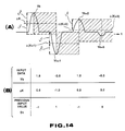
- the so called Furguson's Algorithm is used in such decoding process, and the effect of this process is illustrated in Fig. 13.
- each of the Viterbi decoding circuit 40 and 41 comprises adders 50 and 51, comparator circuits 53 and 55, a latch 54, a data memory circuit 60, a control circuit 61 and a multiplier 62, connected as shown.
- the latch 54 includes a memory 57 and a switch 58.
- the output of the memory 57 is connected to the comparator 55 which receives ascertained data ⁇ k therefrom and outputs decoding result data D1 (Fig. 13D) related to the input data Yk, when the switch 58 is closed.
- the comparator 53 is arranged to output 1 and -1 value data D3 (Fig. 13B) when switch 58 is closed.
- the adder 51 receives the data D3 outputted by the comparator 53 and permits the ⁇ k data to be renewed.
- ⁇ k is the metrollip difference above the trellis line (Fig. 13C) in each respective state.
- the reason for this is that the initial value of ⁇ k is stored as 0 value data.
- the comparator 53 is arranged to compare the data D2 (Fig. 13B) output from the adder 50, with +/- 1 threshold levels and to convert the same into what shall be referred to as previously input data D3 having the values 1, 0, and -1. the output of comparator 53 is supplied to the multiplier 62 as well as to the adder 51.
- the video signal S V to be recorded is supplied to the A/D converter 22 and converted by the latter into a digital signal D V .
- the digital signal data is compressed in the data compression circuit 24 to approximately 25 [Mbps] to form the compressed data signal D R .
- This signal D R along with the audio signal D A are subject to shuffling and correction in the error correction circuit 26 so as to form recording data D REC .
- the recording data D REC is converted into precoded data D PR in the precode circuit 28 in accordance with equation (2). Then, the data D PR is divided into blocks to each of which a 15 Mhz preamble D P is added in the adding circuit 29. Thus, when the blocks of the data D PR are recorded on the tape 5 by the heads 4A, 4B, the preamble recorded with each block can function as a reference signal.
- the magnetic heads 6A and 6B output a playback signal S R which is passed through the playback amplifier 8, the equalizer circuit 9, the variable gain amplifier 31 and the calculation processing circuit 32 to the A/D converter 37 for providing the data Yk.
- the Viterbi circuits 41 and 40 decode the same and output data signals D PBO and D PBE , respectively.
- the signals D PBO and D PBE are recombined and supplied therefrom to error detection and correction circuit 81, data expansion circuit 82 and the D/A converter 83.
- the D/A converter 83 outputs a playback signal S VPB which is essentially identical to the original input signal S V .
- a playback audio signal S APB is preferably obtained from detection and correction circuit 81.
- a recording and/or reproducing device 20′ is generally similar to the previously described device 20, but omits therefrom the variable gain amplifier 31, comparator 70, switch circuit 71, D/A converter 72 and sample-hold condenser or capacitor 73.
- the device 20′ is shown to have level detection circuits 90 and 92 associated with Viterbi circuits 40′ and 41′, respectively, and arranged to receive the signals D YE and D YO , respectively, from the switching circuit 39.
- each of the level detection circuits 90 and 92 is arranged to receive the data D YE or D YO from the selection circuit 39 and to function as a comparator which compares the values of the leading and trailing edges of the data D YE or D YO respectively, with a predetermined standard level.
- a detection signal SCI indicating that the signal has assumed a high level, is issued to the comparator 53 in the respective one of the Viterbi decoding circuits 40′ and 41′.
- the comparator 53 of each of the Viterbi decoding circuits 40′ and 41′ is operatively connected with the respective level detection circuit 90 or 92, as aforesaid, so as to render variable the slice or decision level at which the comparator switches in response to the signal SCI.
- This enables signal D5 from the comparator 53 to be controlled for correspondingly controlling the output of the adder 51.
- the foregoing affects the output of the latch 54 and thus enables the ⁇ k data to be corrected.
- Fig. 20 provides the same advantageous effects as the previously described embodiment.
- Fig. 1 uses positive and negative direction references D REF1 and D REF2 to determine if the ⁇ k value is in the desired range, and controls the variable gain amplifier 31 in accordance with the error voltage or subject from the converter 72 only when ⁇ k is between D REF1 and D REF2 , it is possible to directly control the gain of amplifier 31 by such error voltage.
- the voltage of the reference level which is used in the A/D converter 37 may be made variable and, following the A/D conversion, the level of the signal from the converter 37 may be held at a predetermined level in a manner which corrects the level of the playback signals.
- the present invention is not necessarily limited in its application to systems which use Class IV type partial response techniques and may find application to other types of video recording devices. Moreover, the present invention is not limited in its application to the recording of video signals on magnetic tape, and may be applied to other signals and other recording media.
Abstract
Description
- The present invention relates generally to a device for reproducing magnetically recorded data and more specifically is directed to an apparatus for reproducing video signals which have been digitized.
- In currently used types of video recording apparatus, the video signal is frequency modulated and then recorded as an analog signal on magnetic tape.
- However, in the case where the video signal is converted into a digital signal prior to recording, it is possible to repeatedly dub or copy the recorded signals without incurring any deterioration in the characteristics thereof.
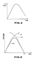
- As shown in Fig. 4, when a signal is reproduced from a magnetic tape, the magnetic head, the tape and the like of the electromagnetic transducing system exhibit characteristics which, in the low frequency and high frequency regions, cause reduction in the S/N ratio.
- Accordingly, depending on the reproducing system, in order to obtain the desired S/N value, a digitized video signal (hereinafter referred to as a digital signal) may be limited to a narrow frequency range. Therefore, it is necessary to use a recording system by which the frequency spectrum enables the S/N ratio to approach its maximum value.
- In order to achieve the above, a method has been proposed wherein the digital signal is recorded by means of a single detection class IV type partial response technique. In other words, as the S/N ratio deteriorates at high and low frequencies, it is possible to use a delay operator D value in the form of a class IV partial response (1-D²) in a manner to proximate the frequency characteristics H(ω), as shown on Fig. 5.
- A video recorder, which ahs been proposed in order to take advantage of the fact that digital video signals can be dubbed without undergoing any deterioration, is shown on Fig. 19. In this arrangement, predetermined recording data DREC is supplied via an
amplifier 3 to amagnetic recording head 4 and recorded thereby onmagnetic tape 5. During reproduction, amagnetic playback head 6 is used to reproduce a signal SRF which is supplied through anamplifier 8 and an equalizingcircuit 9 to adecoding circuit 10. - A clock signal Sck is produced by a
clock signal generator 12 and supplied to thedecoding circuit 10. Thedecoding circuit 10 responds thereto by checking the level of the reproduced signal SRF with respect to a predetermined reference value, at a predetermined timing, and outputting reproduction characteristic data DRB which is then used to decode the digitized video signal. - However, with this arrangement as a result of the movement of the tape and the inherent characteristics of the reproduction system, fluctuations in the level of the signal SRF cannot be avoided.
- If an automatic compensation circuit is provided to correct the level of the signal SRF, a slice level value in the
decoding circuit 10 may become variable and it then becomes necessary to prevent bit error from appearing in the reproduction characteristic data. - However, with the above described method, in the event that noise is contained in the reproduced signal, bit error inevitably occurs.
- Accordingly, it is an object of the present invention to provide a circuit arrangement which can produce a playback or reproduced signal having a minimum amount of bit error which tends to occur due to noise and the like.
- In accordance with an aspect of this invention, there is provided an arrangement having a Viterbi decoding circuit in which, when data falls within a predetermined range, the level of the reproduced signal is sensed and the level of the reproduced signal is corrected in a manner which reduces bit error caused by noise in the reproduced signal.
- In accordance with another aspect of this invention a device for reproducing magnetic recordings features means for recording data on a recording media and for obtaining a reproduced signal therefrom and means for correcting a previous input data value in response to change in an instant input data value.
- In accordance with still another aspect of this invention, a system for recording and reproducing data comprises means for converting an input signal from analog form into digital data; a moving body on which the digital data can be recorded; means for reading the data recorded on the moving body and producing an analog playback signal indicative thereof; means for converting the analog playback signal into a digital playback signal; signal dividing means for separating the digital playback signal into first and second signal portions; first and second Viterbi decoding circuits which respectively receive the first and second signal portions; signal re-combining means for receiving the outputs of the first and second Viterbi decoding circuits and forming a reconstituted digital signal; means for converting the reconstituted digital into an analog output signal; and means associated with the first and second Viterbi decoding circuits for modifying either the output of, or the signal which is input to the first and second viterbi circuits to reduce the bit error in the output of the first and second Viterbi circuits.
- The above, and other objects, features and advantages of this invention, will be apparent in the following detailed description of preferred embodiments thereof which is to be read in connection with the accompanying drawings wherein corresponding components are identified by the same reference numerals in the several views.
-
- Fig. 1 is a block diagram showing a video tape recording device according to a first embodiment of the present invention;
- Figs. 2(A) - 2(E) are timing charts showing the waveforms of various signals which are produced in the circuit arrangement shown in Fig. 1;
- Fig. 3 is a circuit diagram showing details of a precoding circuit used in the device of Fig. 1;
- Fig. 4 is a graph showing, in terms of S/N ratio and frequency, the frequency dependency of the reproduction characteristics;
- Fig. 5 is a graph which demonstrates, in terms of response and frequency, the technique which underlies the Class IV partial response method;
- Fig. 6 is a diagram showing the arrangement of data used in the device of Fig. 1;
- Fig. 7 is a block diagram showing details of a calculation processing circuit utilized in the device shown in Fig. 1;
- Figs. 8 and 9 are diagrams which illustrate the operation of viterbi decoding circuits used in the embodiment of the present invention shown on Fig. 1;
- Figs. 10 and 11 are block diagrams showing equivalence circuits used in electromagnetic recording/reproducing systems embodying this invention;
- Fig. 12 is a block diagram showing the arrangement of a Viterbi decoding circuit in the first embodiment of the present invention;
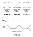
- Figs. 13 to 18 are diagrams which illustrate operation of the Viterbi decoding circuit;
- Fig. 19 is a block diagram showing the arrangement of a previously proposed video tape recorder arrangement;
- Fig. 20 is a block diagram similar to that of Fig. 1, but showing another embodiment of the present invention; and
- Fig. 21 is a block diagram similar to that of Fig. 12, but showing a circuit arrangement which characterizes the embodiment of Fig. 20.
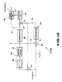
- Referring initially to Fig. 1, it will be seen that a recording and/or reproducing
device 20 according to an embodiment of this invention comprises a recording section having an A/D converter 22, adata compression circuit 24, anerror correction circuit 26, apre-coding circuit 28, anadder 29, anamplifier 30 and recordingheads - The
device 20 further comprises a playback section which includes anamplifier 8, anequalizer circuit 9, avariable gain amplifier 31, acalculation processing circuit 32 and an A/D converter 37 which are also serially connected. A first selection orswitching circuit 39 is connected to the output of the A/D converter 37 and is arranged to selectively switch between first and second Viterbidecoding circuits circuits switching circuit 80 which selectively channels data from the Viterbicircuits correction circuit 81, adata expansion circuit 82 and a D/A converter 83. - A
comparator 70 has one of its three inputs connected to terminals of the Viterbicircuits comparator 70 are connected to sources of reference voltages DREF1 and DREF2, respectively. The output of thecomparator 70 is connected to aswitch circuit 71, which, as shown, is responsive to the output of thecomparator 70 to selectively connect or disconnect an output of a D/A circuit 72 with respect to a gain-control input of thevariable gain amplifier 31. The input of the D/A circuit 72 is connected with the output of the A/D converter 37. A sample andhold condenser 73 is connected between ground and the output terminal of theswitch circuit 71. - In the above described arrangement, the A/
D converter 22 receives an input video signal Sv and is operated in accordance with a clock signal Sck so as to output an 8 bit digital signal Dv each four clock pulses. Thedata compression circuit 24 receives the output Dv of the A/D converter and outputs a data signal DR which is compressed to about 25 [Mbps], and than supplied to the error correction circuit (ECC) 26. - The
ECC circuit 26 is arranged to also receive an audio signal DA in synchronism with the compressed digital signal DR, and shuffles and corrects the received signals prior to outputting a recording data signal DREC (Fig. 2A) of approximately 30 [Mbps]. - As shown in Fig. 3, the
pre-coding circuit 28 may include an exclusive orgate 28A arranged to receive the recording data signal DREC and to output a signal in accordance with a recording clock. Two serially connecteddelay circuits gate 28A with one of its inputs. - The
pre-coding circuit 28 processes the recording data DREC in accordance with the following equation:
- When the value of DREC is between 1 and 0, the changing pre-coding data DPR from the
circuit 28 varies as shown in Fig. 2B. In this instance, MOD2 is a surplus of 2. - Accordingly, as shown in Fig. 4, when a signal is reproduced from a magnetic tape, the magnetic heads and other elements of the electromagnetic transducer system exhibit differential characteristics at low frequencies so that the signal-to-noise S/N ratio drops off markedly and, due to the magnetic characteristics of the tape, the S/N ratio also deteriorates rapidly in the high frequency region. This, of course, limits the frequency range in which a digitized signal, more specifically a digitized video signal, can be reproduced with a suitably high S/N ratio.
- In this connection, it has been proposed to concentrate the frequency spectrum in a range which proximates that at which the S/N ratio is maximized so as to increase the efficiency of the reproduction. In this embodiment, the so called class IV partial response technique is employed in the reproduction of the video signals for that purpose. More specifically, as the S/N ratio deteriorates at high and low frequencies, it is possible as shown in Fig. 5, to employ a delay operator D in the form of a class IV partial response (1 - D²) in a manner to proximate the frequency characteristics H(ω)
- In such case, the minimum response frequencies ω₀ are given by:
ω₀ =
wherein T is the delay time of the operator D and ω₀ is the upper frequency at which the response assumes a minimal value (Fig. 5). - Accordingly, by suitably selecting the value of D (the delay value), the spectrum can be concentrated at the frequencies at which the S/N ratio is maximized.
- The overall transmission frequency is given by:
(1-D) x (1+D) = 1-D² (3) - Accordingly, by setting the transmission function to 1, the calculation control within the
pre-coding circuit 28 can be executed in a manner which improves the efficiency of the reproduction. - Fig. 6 shows that, in a block of pre-coded data DPR from the
circuit 28, the pre-coded data is sandwiched between a preamble and a postamble. In connection with this data formation with a 0,1 connection, the precoded data DPR is, by theamplifier 30, converted to recording signal data DR having for example, -1, 1 values, and is written onto thetape 5. - The
magnetic heads - The preamble is such that the recorded block is recorded at half the frequency (viz., 15 MHz) of the DPR signal which is compressed in a manner to have a frequency of about 30 Mhz, and is used as a reference signal. The frequency of this reference signal is of course selected in accordance with the values of ω₀ obtained from equation (2).
- In the present embodiment, the preamble is used as a clock signal which determines the control of the playback signal SRF from the
equalizer circuit 9. -
Magnetic heads tape 5 are arranged to respond to the preamble and postamble data and to read the recorded data and output a playback signal SR (fig. 2C). This signal SR is supplied through theamplifier 8,equalizer circuit 9 andvariable gain amplifier 31 to the calculation orprocessing circuit 32. As shown in Fig. 7, theprocessing circuit 32 may comprise anadder circuit 34 and adelay circuit 35. In this arrangement, the signal SRF from theequalizer circuit 9 is processed with respect to (1+D). As a result of the foregoing, and as the electromagnetic reproduction or playback system exhibits differential characteristics so that the signal SRF has the delay operator D applied thereto in the form of (1-D), the effect shown in Fig. 5 is obtained. - Accordingly, for the purpose of accommodating the reproduction characteristics, at the time of recording of the pre-coded data, correction is effected in accordance with equation (3) and the efficiency of the recording of the video signal is improved.
- Due to the provision of the
processing circuit 32, the amplitude of the output signal SF (Fig. 2D) therefrom can be varied in accordance with the logic level. - The A/
D circuit 37 receives the signal SF in accordance with the reproduction clock and converts the signal SF into digital data Yk output to theselection circuit 39. - The
selection circuit 39 switches from one terminal to the other so that the output data Yk is selectively outputted fromcircuit 39 as even number data DYE and odd number data DYO which are respectively supplied to theViterbi decoding circuits - As shown in Figs. 8 and 9, the processing of signal SRF with respect to (1-D²) is such that serial values bn, bn+1...represent the recording signal DR at a doubled clock pulse frequency used to divide the odd number frequency and even number frequency data Yk input to the
selection circuit 39 and renders it possible to process the odd and even number frequency data with respect to (1-D). - By reason of the foregoing, when noise SN enters the electromagnetic reproduction system, for example, through the
magnetic heads magnetic tape 5, as shown in Fig. 10, it is possible to process the recording signal DR with respect to (1-D²) in aprocessing circuit 45 so as to form an output signal SF which may be equivalently written together with the noise signal SN as an output signal SR from anadder circuit 46. - When the signal SF is divided into odd number and even number frequency streams, it is possible to process the recording signal DR with respect to (1-D) in a processing circuit 47 (Fig. 11) so as to form an output signal SF which may be equivalently written with a noise signal SN as an output signal SR from an
adder circuit 48. - When the recording signal DR which is divided between the odd and even lines is coded and the (1-D) correlation between the Yk, YK+1.... data is used, the bit error reduced reproduction data DPB can be decoded in accordance with the detected noise SN which has been previously added to the signal. The so called Furguson's Algorithm is used in such decoding process, and the effect of this process is illustrated in Fig. 13.
- As shown in Fig. 12, in the embodiment being presently described, each of the
Viterbi decoding circuit adders comparator circuits latch 54, adata memory circuit 60, acontrol circuit 61 and amultiplier 62, connected as shown. - The
latch 54 includes amemory 57 and aswitch 58. The output of thememory 57 is connected to thecomparator 55 which receives ascertained data Δk therefrom and outputs decoding result data D1 (Fig. 13D) related to the input data Yk, when theswitch 58 is closed. - The
comparator 53 is arranged tooutput 1 and -1 value data D3 (Fig. 13B) whenswitch 58 is closed. Theadder 51 receives the data D3 outputted by thecomparator 53 and permits the Δk data to be renewed. - At this point, Δk is the metrollip difference above the trellis line (Fig. 13C) in each respective state. The reason for this is that the initial value of Δk is stored as 0 value data.
- The
comparator 53 is arranged to compare the data D2 (Fig. 13B) output from theadder 50, with +/- 1 threshold levels and to convert the same into what shall be referred to as previously input data D3 having thevalues comparator 53 is supplied to themultiplier 62 as well as to theadder 51. - The relationship between data Δk and the input data Yk+1 is given by the following equation:
Δk -Yk+ 1 > 1 (4) - When the previously input data D3 is set at a level of 1, the
adder 51 outputs a signal Δ(k+1) in accordance with the following equation:
Δ(k+1) = Yk+1 + 1 (5) - This value is stored in the
memory 57 and thus renews the Δk data. In this connection the following relationship is established.
Δk -Yk+ 1 < -1 (6) - Accordingly, the data Δk which is stored in the
memory 57 when D3 exhibits a -1 value, is such that
A(k+1) = Yk+1 - 1 (7)
and the Δk data is renewed. - Further, given that
| Δk - Yk+1 | < 1 (8)
when D3 is set to 0, Δk is given by
Δ(k+1) = Δk (9) - As conventional Viterbi circuits are used in the present embodiment and as the operation and underlying theory of the operation is well documented, further detailed disclosure of the same will be omitted for the sake of brevity. However, for further information reference may be had to:
- 1. The Viterbi Algorithm - an Invited Paper by G. David Forney, Jr. - published in PROCEEDINGS OF THE IEEE, VOL. 6 No. 3 March 1973;
- 2. The Effects of Nonlinear Distortion on Class IV Partial Response by Paul Mewby and Roger Wood of the Ampex Corporation, Redwood city, California - published in IEEE TRANSACTIONS ON MAGNETICS, Vol. Mag-22, No. 5 September 1986; and
- 3. Application of Partial-response Channel Coding to Magnetic Recording Systems by H. Kobayashi and D.T. Tang - published in IMB J. RES. DEVELOP July 1970.
- The operation of the first described embodiment of the invention will be further explained below:
- The video signal SV to be recorded is supplied to the A/
D converter 22 and converted by the latter into a digital signal DV. The digital signal data is compressed in thedata compression circuit 24 to approximately 25 [Mbps] to form the compressed data signal DR. This signal DR along with the audio signal DA are subject to shuffling and correction in theerror correction circuit 26 so as to form recording data DREC. - The recording data DREC is converted into precoded data DPR in the
precode circuit 28 in accordance with equation (2). Then, the data DPR is divided into blocks to each of which a 15 Mhz preamble DP is added in the addingcircuit 29. Thus, when the blocks of the data DPR are recorded on thetape 5 by theheads - In response to such reference signal, in the playback mode of the
device 20, themagnetic heads playback amplifier 8, theequalizer circuit 9, thevariable gain amplifier 31 and thecalculation processing circuit 32 to the A/D converter 37 for providing the data Yk. Following the division of the data Yk into the odd and even frequency number streams DYO and DYE by the switchingcircuit 39, theViterbi circuits - In response to the data Yk, data Δk is renewed so that, when the output data Yk is "1", a comparison of Δk with the first and second reference levels DREF1 and DREF2, is carried out. When the level of Δk falls between DREF1 and DREF2 the analog signal which is produced in the D/
A converter 72 is supplied throughswitch circuit 71 to the sample-hold capacitor 73. Thus when the Δk data output of the Viterbi decoding circuit is "1" and falls between the reference levels DREF1 and DREF2, checking of the level of the playback signal SRF is induced. The gain of thevariable gain amplifier 31 is varied depending on the voltage appearing on the sample-hold capacitor 73. The foregoing ensures that the level of signals SRF, which are output by thevariable gain amplifier 31, is maintained at a predetermined level. - Even when noise is mixed in with the signal SRF since the level thereof is held at a predetermined level, the bit error in signals DPBO and DPBE can be reduced.
- At
selection circuit 80, the signals DPBO and DPBE are recombined and supplied therefrom to error detection andcorrection circuit 81,data expansion circuit 82 and the D/A converter 83. The D/A converter 83 outputs a playback signal SVPB which is essentially identical to the original input signal SV. - Further, a playback audio signal SAPB is preferably obtained from detection and
correction circuit 81. - Referring now to Fig. 20, it will be seen that a recording and/or reproducing
device 20′ according to another embodiment of this invention is generally similar to the previously describeddevice 20, but omits therefrom thevariable gain amplifier 31,comparator 70,switch circuit 71, D/A converter 72 and sample-hold condenser orcapacitor 73. - In place of the foregoing elements in the
device 20, thedevice 20′ is shown to havelevel detection circuits Viterbi circuits 40′ and 41′, respectively, and arranged to receive the signals DYE and DYO, respectively, from the switchingcircuit 39. - As shown in Fig. 21 each of the
level detection circuits selection circuit 39 and to function as a comparator which compares the values of the leading and trailing edges of the data DYE or DYO respectively, with a predetermined standard level. - In the present embodiment, when the leading and trailing edge values of the data DYE or DYO exceed a value of 1.5, a detection signal SCI, indicating that the signal has assumed a high level, is issued to the
comparator 53 in the respective one of theViterbi decoding circuits 40′ and 41′. - The
comparator 53 of each of theViterbi decoding circuits 40′ and 41′ is operatively connected with the respectivelevel detection circuit comparator 53 to be controlled for correspondingly controlling the output of theadder 51. Of course, the foregoing affects the output of thelatch 54 and thus enables the Δk data to be corrected. - Accordingly, the embodiment of Fig. 20 provides the same advantageous effects as the previously described embodiment.
- Although the embodiment described with reference to Fig. 1 uses positive and negative direction references DREF1 and DREF2 to determine if the Δk value is in the desired range, and controls the
variable gain amplifier 31 in accordance with the error voltage or subject from theconverter 72 only when Δk is between DREF1 and DREF2, it is possible to directly control the gain ofamplifier 31 by such error voltage. - Further, the voltage of the reference level which is used in the A/
D converter 37 may be made variable and, following the A/D conversion, the level of the signal from theconverter 37 may be held at a predetermined level in a manner which corrects the level of the playback signals. - Furthermore, it is to be noted that the present invention is not necessarily limited in its application to systems which use Class IV type partial response techniques and may find application to other types of video recording devices. Moreover, the present invention is not limited in its application to the recording of video signals on magnetic tape, and may be applied to other signals and other recording media.
- Having specifically described preferred embodiments of the invention with reference to the accompanying drawings, it is to be understood that the invention is not limited to those embodiments or to the specifically mentioned modifications thereof, and that various changes and modifications may be effected therein by one skilled in the art without departing from the scope or spirit of the invention as defined in the appended claims.
Claims (8)
a video signal circuit comprising:
means for recording data on a recording media and for obtaining a reproduced signal from said recording media; and
means responsive to a change in the value of instant input data for correcting the value of a prior input data.
means for reproducing the recorded data;
Viterbi decoding circuit means for decoding the reproduced data;
detecting means for detecting the level of decoded reproduced data output from said Viterbi decoding circuit means;
means for comparing the detected level of the decoded reproduced data with a predetermined level;
means for determining if the compared detected level falls within a predetermined range; and
means for correcting the level of the decoded data which falls within said predetermined range.
means for converting an input signal from analog form to the form of digital data;
a moving magnetic recording medium;
means for magnetically recording said data on said record medium;
means for reading data recorded on said moving medium and producing an analog playback signal indicative thereof;
means for converting said analog playback signal into a digital playback signal;
signal dividing means for dividing said digital playback signal into first and second signal portions;
first and second Viterbi decoding circuits which respectively receive said first and second signal portions;
signal re-combining means for receiving outputs of said first and second Viterbi decoding circuits and forming a reconstituted digital signal therefrom;
means for converting said reconstituted digital signal into an analog output signal; and
modifying means associated with said first and second Viterbi decoding circuits for modifying either the outputs of said first and second Viterbi circuits or the signal portions respectively received by said Viterbi decoding circuits so as to reduce the bit error in the outputs of said first and second Viterbi circuits.
comparator means operatively connected with said first and second Viterbi decoding circuits in a manner to receive data which indicates differences between values of sequentially received signal portions, said comparator means being operative to compare said difference indicating data with a reference value, and a variable gain amplifier connected with said comparator means and arranged between said means for reading the data recorded on said moving recording medium and producing an analog playback signal indicative thereof and said means for converting the analog playback signal into a digital playback signal.
an input terminal for receiving the respective one of said signal portions;
first and second adders having respective inputs connected with said input terminal and further having respective outputs;
multiplier means;
first and second comparators having respective outputs connected to said multiplier means;
latch means including a memory, a latch input connected to said output of the second adder and a latch output connected to inputs of said second comparator and said first adder, said output of the first adder being connected to an input of said first comparator, and said output of the first comparator being connected to another input of said second adder;
a control circuit connected to an output of said multiplier; and
a data memory circuit having a first input connected with said output of the second comparator and a second input connected with an output of said control circuit.
level detection means for detecting the level of said respective signal portion, said level detection means having an output which is connected to another input of said first comparator, said first comparator being responsive to said level detection means in a manner to change a decision level therein.
a third comparator operatively connected with said latch output; and
variable gain amplifier means controllable by an output from said third comparator and arranged between said means for reading the recorded data and producing an analog playback signal indicative thereof and said means for converting the analog playback signal into a digital playback signal.
Applications Claiming Priority (4)
| Application Number | Priority Date | Filing Date | Title |
|---|---|---|---|
| JP47793/89 | 1989-02-28 | ||
| JP1047793A JP2784786B2 (en) | 1989-02-28 | 1989-02-28 | Magnetic recording / reproducing device |
| JP139654/89 | 1989-05-31 | ||
| JP1139654A JP2853171B2 (en) | 1989-05-31 | 1989-05-31 | Magnetic recording / reproducing device |
Publications (3)
| Publication Number | Publication Date |
|---|---|
| EP0385867A2 true EP0385867A2 (en) | 1990-09-05 |
| EP0385867A3 EP0385867A3 (en) | 1992-06-17 |
| EP0385867B1 EP0385867B1 (en) | 1997-04-16 |
Family
ID=26387964
Family Applications (1)
| Application Number | Title | Priority Date | Filing Date |
|---|---|---|---|
| EP90400566A Expired - Lifetime EP0385867B1 (en) | 1989-02-28 | 1990-02-28 | Digital signal reproducing apparatus |
Country Status (4)
| Country | Link |
|---|---|
| US (1) | US5270876A (en) |
| EP (1) | EP0385867B1 (en) |
| AU (1) | AU629300B2 (en) |
| DE (1) | DE69030460T2 (en) |
Cited By (6)
| Publication number | Priority date | Publication date | Assignee | Title |
|---|---|---|---|---|
| EP0445780A2 (en) * | 1990-03-07 | 1991-09-11 | Canon Kabushiki Kaisha | Image signal recording and reproducing system |
| EP0534651A1 (en) * | 1991-09-27 | 1993-03-31 | Hewlett-Packard Company | Signal processing system for adaptive equalization |
| EP0684605A1 (en) * | 1994-05-23 | 1995-11-29 | STMicroelectronics S.r.l. | Parallel architecture PRML device for processing signals from a magnetic head during a reading step of data stored on a magnetic support |
| EP0758784A2 (en) * | 1995-08-16 | 1997-02-19 | Nikon Corporation | Information regenerating apparatus |
| US5661709A (en) * | 1993-04-06 | 1997-08-26 | Matsushita Electric Industrial Co., Ltd. | Digital signal detection circuit |
| US6078462A (en) * | 1994-05-23 | 2000-06-20 | Stmicroelectronics, S.R.L. | Device and method for processing servo signals in a parallel architecture PRML reading apparatus for hard disks |
Families Citing this family (8)
| Publication number | Priority date | Publication date | Assignee | Title |
|---|---|---|---|---|
| JP3259302B2 (en) * | 1992-01-28 | 2002-02-25 | 株式会社日立製作所 | Output signal decoding method and apparatus |
| JPH06231406A (en) * | 1993-02-04 | 1994-08-19 | Hitachi Ltd | Method and device for magnetic recording and reproducing |
| US5602858A (en) * | 1993-09-20 | 1997-02-11 | Kabushiki Kaisha Toshiba | Digital signal decoding apparatus having a plurality of correlation tables and a method thereof |
| EP0644661B1 (en) * | 1993-09-20 | 2000-06-14 | Canon Kabushiki Kaisha | Signal processing apparatus |
| JP3237974B2 (en) * | 1993-09-20 | 2001-12-10 | 株式会社東芝 | Digital signal decoding device |
| JPH08329619A (en) * | 1994-10-27 | 1996-12-13 | Hitachi Ltd | Method and device for producing data and data reproducing circuit |
| JP3475627B2 (en) * | 1995-12-22 | 2003-12-08 | ソニー株式会社 | Digital signal reproducing apparatus and reproducing method |
| JP2005166221A (en) * | 2003-12-05 | 2005-06-23 | Canon Inc | Information reproducing method and apparatus |
Citations (2)
| Publication number | Priority date | Publication date | Assignee | Title |
|---|---|---|---|---|
| US4321618A (en) * | 1978-07-19 | 1982-03-23 | Hitachi, Ltd. | Reproducing system for video tape recorders |
| JPS62135018A (en) * | 1985-12-06 | 1987-06-18 | Fujitsu Ltd | Viterbi decoder |
Family Cites Families (4)
| Publication number | Priority date | Publication date | Assignee | Title |
|---|---|---|---|---|
| DE3676825D1 (en) * | 1986-08-05 | 1991-02-14 | Ibm | AMPLIFIER CONTROL CIRCUIT FOR A PLAYBACK DEVICE IN A MAGNETIC RECORDING SYSTEM USING A PARTIAL PLAYBACK METHOD AND THE HIGHEST PROBABILITY. |
| US4991034A (en) * | 1987-12-11 | 1991-02-05 | Sanyo Electric Co., Ltd. | DC restoration circuit for restoring and compensating a low frequency component lost in a digital signal |
| US5095392A (en) * | 1988-01-27 | 1992-03-10 | Matsushita Electric Industrial Co., Ltd. | Digital signal magnetic recording/reproducing apparatus using multi-level QAM modulation and maximum likelihood decoding |
| JP2629238B2 (en) * | 1988-02-05 | 1997-07-09 | ソニー株式会社 | Decoding device and decoding method |
-
1990
- 1990-02-19 AU AU49915/90A patent/AU629300B2/en not_active Expired
- 1990-02-20 US US07/482,302 patent/US5270876A/en not_active Expired - Lifetime
- 1990-02-28 EP EP90400566A patent/EP0385867B1/en not_active Expired - Lifetime
- 1990-02-28 DE DE69030460T patent/DE69030460T2/en not_active Expired - Lifetime
Patent Citations (2)
| Publication number | Priority date | Publication date | Assignee | Title |
|---|---|---|---|---|
| US4321618A (en) * | 1978-07-19 | 1982-03-23 | Hitachi, Ltd. | Reproducing system for video tape recorders |
| JPS62135018A (en) * | 1985-12-06 | 1987-06-18 | Fujitsu Ltd | Viterbi decoder |
Non-Patent Citations (5)
| Title |
|---|
| IBM JOURNAL OF RESEARCH AND DEVELOPMENT. vol. 14, no. 4, July 1970, NEW YORK US pages 368 - 375; H. KOBAYASHI ET AL.: 'Application of partial-response channel coding to magnetic recording systems' * |
| IEEE TRANSACTIONS ON CONSUMER ELECTRONICS. vol. 34, no. 3, August 1988, NEW YORK US pages 434 - 441; Y. KUBO ET AL.: 'Development of a VTR video signal processing IC' * |
| IEEE TRANSACTIONS ON CONSUMER ELECTRONICS. vol. 34, no. 3, August 1988, NEW YORK US pages 588 - 595; C. YAMAMITSU ET AL.: 'An experimental study on bit rate reduction and high density recording for a home-use digital VTR' * |
| PATENT ABSTRACTS OF JAPAN vol. 11, no. 359 (E-559)21 November 1987 & JP-A-62 135 018 ( MASARU ET AL. ) 18 June 1987 * |
| SMPTE JOURNAL. vol. 97, no. 1, January 1988, US pages 8 - 12; S. MITA ET AL.: 'Adaptive equalization techniques for digital video recording systems' * |
Cited By (9)
| Publication number | Priority date | Publication date | Assignee | Title |
|---|---|---|---|---|
| EP0445780A2 (en) * | 1990-03-07 | 1991-09-11 | Canon Kabushiki Kaisha | Image signal recording and reproducing system |
| EP0445780A3 (en) * | 1990-03-07 | 1993-06-09 | Canon Kabushiki Kaisha | Image signal recording and reproducing system |
| EP0534651A1 (en) * | 1991-09-27 | 1993-03-31 | Hewlett-Packard Company | Signal processing system for adaptive equalization |
| US5661709A (en) * | 1993-04-06 | 1997-08-26 | Matsushita Electric Industrial Co., Ltd. | Digital signal detection circuit |
| EP0684605A1 (en) * | 1994-05-23 | 1995-11-29 | STMicroelectronics S.r.l. | Parallel architecture PRML device for processing signals from a magnetic head during a reading step of data stored on a magnetic support |
| US6067198A (en) * | 1994-05-23 | 2000-05-23 | Stmicroelectronics S.R.L. | Apparatus and method for processing a data signal from a magnetic-media reading head |
| US6078462A (en) * | 1994-05-23 | 2000-06-20 | Stmicroelectronics, S.R.L. | Device and method for processing servo signals in a parallel architecture PRML reading apparatus for hard disks |
| EP0758784A2 (en) * | 1995-08-16 | 1997-02-19 | Nikon Corporation | Information regenerating apparatus |
| EP0758784A3 (en) * | 1995-08-16 | 1998-06-03 | Nikon Corporation | Information regenerating apparatus |
Also Published As
| Publication number | Publication date |
|---|---|
| EP0385867A3 (en) | 1992-06-17 |
| AU629300B2 (en) | 1992-10-01 |
| AU4991590A (en) | 1990-09-06 |
| DE69030460T2 (en) | 1997-07-24 |
| EP0385867B1 (en) | 1997-04-16 |
| US5270876A (en) | 1993-12-14 |
| DE69030460D1 (en) | 1997-05-22 |
Similar Documents
| Publication | Publication Date | Title |
|---|---|---|
| US5270876A (en) | Apparatus for reproducing data recorded on a magnetic recording medium | |
| US5404248A (en) | Video data recording/reproducing apparatus with efficient error correction | |
| US4367495A (en) | Method and apparatus for magnetic recording and reproduction of digital signal | |
| US5255128A (en) | Apparatus for detecting digital data | |
| JPH01102777A (en) | Digital signal recording and reproducing device | |
| US5361174A (en) | Magnetic reproducing apparatus | |
| KR0170261B1 (en) | The most appropriate recording/reproducing apparatus | |
| KR100213032B1 (en) | Device for detecting digital signals in a magnetic recording reproducing device | |
| US6266378B1 (en) | Data detector and data detection method which measure and correct for phase differences between a sampling point and an optimal detection point | |
| US6278749B1 (en) | Data detector and method for detecting data | |
| US6263148B1 (en) | Variable-mode information signal reproduction apparatus with tracking control | |
| US6374035B1 (en) | Signal processing device | |
| EP0445780B1 (en) | Image signal recording and reproducing system | |
| KR100202208B1 (en) | Digital signal reproducing apparatus | |
| KR100202209B1 (en) | Digital signal reproducing apparatus | |
| JPH07296524A (en) | Digital data reproducing device | |
| Yamamitsu et al. | An experimental study on bit rate reduction and high density recording for a home-use digital VTR | |
| JP2822264B2 (en) | Automatic gain control circuit | |
| JPH0793899A (en) | Magnetic recording and reproducing device | |
| JPH06325308A (en) | Reproducing device for digital information | |
| JP2917191B2 (en) | Digital signal reproduction device | |
| JPH04216303A (en) | Digital-signal recording/regenerating circuit for video recorder | |
| JPS63113982A (en) | Digital signal detecting circuit | |
| KR0151030B1 (en) | Digital recording-reproducing device with equalizer in common | |
| JPH06140875A (en) | Automatic equalizer |
Legal Events
| Date | Code | Title | Description |
|---|---|---|---|
| PUAI | Public reference made under article 153(3) epc to a published international application that has entered the european phase |
Free format text: ORIGINAL CODE: 0009012 |
|
| AK | Designated contracting states |
Kind code of ref document: A2 Designated state(s): DE FR GB |
|
| PUAL | Search report despatched |
Free format text: ORIGINAL CODE: 0009013 |
|
| AK | Designated contracting states |
Kind code of ref document: A3 Designated state(s): DE FR GB |
|
| 17P | Request for examination filed |
Effective date: 19921005 |
|
| 17Q | First examination report despatched |
Effective date: 19940812 |
|
| GRAG | Despatch of communication of intention to grant |
Free format text: ORIGINAL CODE: EPIDOS AGRA |
|
| GRAH | Despatch of communication of intention to grant a patent |
Free format text: ORIGINAL CODE: EPIDOS IGRA |
|
| GRAH | Despatch of communication of intention to grant a patent |
Free format text: ORIGINAL CODE: EPIDOS IGRA |
|
| GRAA | (expected) grant |
Free format text: ORIGINAL CODE: 0009210 |
|
| AK | Designated contracting states |
Kind code of ref document: B1 Designated state(s): DE FR GB |
|
| REF | Corresponds to: |
Ref document number: 69030460 Country of ref document: DE Date of ref document: 19970522 |
|
| ET | Fr: translation filed | ||
| PLBE | No opposition filed within time limit |
Free format text: ORIGINAL CODE: 0009261 |
|
| STAA | Information on the status of an ep patent application or granted ep patent |
Free format text: STATUS: NO OPPOSITION FILED WITHIN TIME LIMIT |
|
| 26N | No opposition filed | ||
| REG | Reference to a national code |
Ref country code: GB Ref legal event code: IF02 |
|
| PGFP | Annual fee paid to national office [announced via postgrant information from national office to epo] |
Ref country code: DE Payment date: 20090226 Year of fee payment: 20 |
|
| PGFP | Annual fee paid to national office [announced via postgrant information from national office to epo] |
Ref country code: GB Payment date: 20090225 Year of fee payment: 20 |
|
| PGFP | Annual fee paid to national office [announced via postgrant information from national office to epo] |
Ref country code: FR Payment date: 20090213 Year of fee payment: 20 |
|
| REG | Reference to a national code |
Ref country code: GB Ref legal event code: PE20 Expiry date: 20100227 |
|
| PG25 | Lapsed in a contracting state [announced via postgrant information from national office to epo] |
Ref country code: GB Free format text: LAPSE BECAUSE OF EXPIRATION OF PROTECTION Effective date: 20100227 |
|
| PG25 | Lapsed in a contracting state [announced via postgrant information from national office to epo] |
Ref country code: DE Free format text: LAPSE BECAUSE OF EXPIRATION OF PROTECTION Effective date: 20100228 |