EP0617409A2 - Method of manufacturing a thin-film magnetic head, and magnetic head obtainable by means of said method - Google Patents
Method of manufacturing a thin-film magnetic head, and magnetic head obtainable by means of said method Download PDFInfo
- Publication number
- EP0617409A2 EP0617409A2 EP94200675A EP94200675A EP0617409A2 EP 0617409 A2 EP0617409 A2 EP 0617409A2 EP 94200675 A EP94200675 A EP 94200675A EP 94200675 A EP94200675 A EP 94200675A EP 0617409 A2 EP0617409 A2 EP 0617409A2
- Authority
- EP
- European Patent Office
- Prior art keywords
- layer
- magnetic material
- soft
- magnetic
- main
- Prior art date
- Legal status (The legal status is an assumption and is not a legal conclusion. Google has not performed a legal analysis and makes no representation as to the accuracy of the status listed.)
- Granted
Links
Images


Classifications
-
- G—PHYSICS
- G11—INFORMATION STORAGE
- G11B—INFORMATION STORAGE BASED ON RELATIVE MOVEMENT BETWEEN RECORD CARRIER AND TRANSDUCER
- G11B5/00—Recording by magnetisation or demagnetisation of a record carrier; Reproducing by magnetic means; Record carriers therefor
- G11B5/127—Structure or manufacture of heads, e.g. inductive
- G11B5/33—Structure or manufacture of flux-sensitive heads, i.e. for reproduction only; Combination of such heads with means for recording or erasing only
- G11B5/39—Structure or manufacture of flux-sensitive heads, i.e. for reproduction only; Combination of such heads with means for recording or erasing only using magneto-resistive devices or effects
- G11B5/3903—Structure or manufacture of flux-sensitive heads, i.e. for reproduction only; Combination of such heads with means for recording or erasing only using magneto-resistive devices or effects using magnetic thin film layers or their effects, the films being part of integrated structures
- G11B5/3906—Details related to the use of magnetic thin film layers or to their effects
- G11B5/3916—Arrangements in which the active read-out elements are coupled to the magnetic flux of the track by at least one magnetic thin film flux guide
- G11B5/3919—Arrangements in which the active read-out elements are coupled to the magnetic flux of the track by at least one magnetic thin film flux guide the guide being interposed in the flux path
- G11B5/3922—Arrangements in which the active read-out elements are coupled to the magnetic flux of the track by at least one magnetic thin film flux guide the guide being interposed in the flux path the read-out elements being disposed in magnetic shunt relative to at least two parts of the flux guide structure
- G11B5/3925—Arrangements in which the active read-out elements are coupled to the magnetic flux of the track by at least one magnetic thin film flux guide the guide being interposed in the flux path the read-out elements being disposed in magnetic shunt relative to at least two parts of the flux guide structure the two parts being thin films
-
- Y—GENERAL TAGGING OF NEW TECHNOLOGICAL DEVELOPMENTS; GENERAL TAGGING OF CROSS-SECTIONAL TECHNOLOGIES SPANNING OVER SEVERAL SECTIONS OF THE IPC; TECHNICAL SUBJECTS COVERED BY FORMER USPC CROSS-REFERENCE ART COLLECTIONS [XRACs] AND DIGESTS
- Y10—TECHNICAL SUBJECTS COVERED BY FORMER USPC
- Y10T—TECHNICAL SUBJECTS COVERED BY FORMER US CLASSIFICATION
- Y10T29/00—Metal working
- Y10T29/49—Method of mechanical manufacture
- Y10T29/49002—Electrical device making
- Y10T29/4902—Electromagnet, transformer or inductor
- Y10T29/49021—Magnetic recording reproducing transducer [e.g., tape head, core, etc.]
- Y10T29/49032—Fabricating head structure or component thereof
- Y10T29/49048—Machining magnetic material [e.g., grinding, etching, polishing]
Definitions
- the invention relates to a method of manufacturing a thin-film magnetic head comprising a magnetoresistive element and at least one flux guide, which method starts from a support.
- the magnetic heads obtained by means of the methods described in EP-A 0 516-022 are integrated magnetic heads having a contact face and comprising an inductive part and a magnetoresistive part.
- a first structured insulation layer of Si0 2 is formed on a magnetic substrate of a ferrite by means of a lithographic method, which layer is subsequently provided with a layer of Au for forming a write coil.
- a second structured insulation layer is provided on which a core layer of an amorphous material based on Co is deposited. This core layer is in contact with the magnetic substrate via apertures in the insulation layers.
- the parts of the second insulation layer not coated by the core layer are filled up by means of a filling layer of A1 2 0 3 . After the filling layer has been formed, the core layer and the filling layer are planed by means of lapping.
- a third structured insulation layer of Si0 2 is deposited on the surface thus obtained on which subsequently a bias winding of Au is formed.
- a fourth structured insulation layer of Si0 2 is provided on this winding.
- a magnetoresistive element of permalloy is formed on this insulation layer.
- a fifth structured insulation layer of Si0 2 is provided and subsequently a yoke of an amorphous material which is based on Co and is in contact with the core layer via apertures in the three last-mentioned insulation layers.
- two flux guides of a Co- based amorphous material are provided on a non-magnetic substrate, while an aperture between the two flux guides is filled with a first insulation layer of Si0 2 .
- the surface formed by the flux guides and the first insulation layer is provided with a second structured insulation layer on which subsequently a magnetoresistive (MR) element is formed.
- the MR element is then coated with a third structured insulation layer on which subsequently a bias winding is formed.
- a fourth structured insulation layer is provided for the purpose of coating the bias winding.
- a magnetic core layer of a Co- based material is formed which is in contact with one of the flux guides via apertures in the three last-mentioned insulation layers.
- the areas not coated by the first core layer are filled up with a filling layer of AI 2 0a, whereafter a surface on which an inductive head part is formed is obtained by lapping.
- the MR element is formed on an insulation layer which is provided on a lapping-processed surface.
- a surface extending on two or more adjacent layers of different material has unevennesses.
- damage particularly in the form of scratches in and disturbances of material under the surface obtained are caused by lapping.
- Such a surface is inadmissible, inefficient for information transfer and may increase the risk of instabilities in the MR element provided on said surface.
- the magnetic heads obtained by the methods known from EP-A 0 516 022 have the further drawback that due to the presence of irregularities on the surface engaging the MR element, a relatively thick insulation layer is required between the MR element and the electrically conducting flux guides so as to ensure a reliable electrical insulation between the MR element and the flux guides.
- insulation layers have a further negative influence on the efficiency of the magnetic heads. For various reasons, damage in and material disturbance under a surface above which the MR element is present are thus undesirable.
- the method according to the invention is therefore characterized in that a main layer of a non-magnetic material is formed on the support, which layer is provided with a recess by removing material from a side remote from the support, said recess being subsequently filled up with a soft-magnetic material for forming the flux guide, whereafter the main layer provided with the filled recess is mechanochemically polished for forming a main surface at which subsequently a layer of a magnetoresistive material is provided for forming the magnetoresistive element.
- the magnetic flux guide is provided in the main layer which itself is non-magnetic. Consequently, the mechanochemical polishing operation is performed on soft-magnetic material as well as on non-magnetic material. It has surprisingly been found that despite the different material properties between the soft-magnetic and the non-magnetic material the mechanochemical polishing operation yields a very plane and smooth main surface without the materials themselves being subject to structural changes.
- a polished, plane surface which is free from damage is obtained for the purpose of providing the magnetoresistive element (MR element) in an electrically insulated manner, which results in a magnetic head having a stable MR element and an efficiency which is improved with respect to that of the known magnetic heads.
- MR element magnetoresistive element
- mechanochemical polishing is performed with the aid of a working surface of a polishing tool which is urged against and moved across the surface to be polished.
- the working surface is provided with a liquid mechanochemical polishing agent.
- This is an agent with which chemical and mechanical polishing is simultaneously possible.
- polishing without damage can be realised by purely chemical polishing.
- This method has drawbacks.
- the geometrical control, i.e. the planeness of the surface is far from optimal and many chemical polishing agents are more or less toxic and aggressive and should consequently be used in an extremely protected environment, which is a drawback in mass production.
- the mechanochemical polishing operation in which components mechanically removed from the surface to be polished are chemically dissolved, leads to a very smooth and plane polished surface which is free from damage. It has surprisingly been found that if one of the components to be polished is very hard, the mechanical aspect of mechanochemically polishing will be enhanced by adding a small quantity of hard, adequate grains to the polishing agent of the mechanochemical type. Thus, even when very hard materials are used in the manufacture of heads, a smooth and plane surface which is free from damage can be realised.
- An embodiment of the method according to the invention is characterized in that a plate-shaped substrate is used as a support which is provided with two parallel substrate faces by means of mechanical and/or mechanochemical polishing, whereafter the main layer is formed on one of these faces.
- the other face is used as a reference face in the further process steps.
- the parallel substrate faces may be obtained by starting from a substrate having two substrate faces, the substrate faces being first prepared by means of polishing until they have a convex, plane or concave initial shape, whereafter a removal cycle is run through at least once, during which the substrate faces of a substrate whose edges are thicker than a central piece surrounded by the edges are polished in such a way that the edges successively acquire a substantially equal thickness, a smaller thickness and again a substantially equal thickness as the central piece, and during which cycle the substrate faces of a substrate whose edges are thinner than a central piece surrounded by the edges are polished in such a way that the edges successively acquire a substantially equal thickness, a larger thickness and again a substantially equal thickness as the central piece.
- the above-mentioned method of manufacturing parallel faces is described extensively in European Patent Application 92201739.7 (PHN 14.081 EP-P; herewith incorporated by reference).
- Substrates having parallel substrate faces have the great advantage that they can be used in a mass manufacturing process for the further steps of the method. Consequently, mechanochemical polishing steps can be performed at a later stage for the purpose of smoothing and planing a layer having a single or multiple material structure and for stop-polishing a layer having a multiple material structure, but of which only one or some materials of the layer can be polished via the mechanochemical polishing process and the other material cannot be polished.
- An embodiment of the method is characterized in that the support is formed from a soft-magnetic material, particularly a ferrite.
- a ferrite is understood to be a magnetic material of, for example one of the following crystallographic groups: garnets, spinels, perovskites. Favourable properties of ferrite are its great wear resistance and its satisfactory shielding effect against disturbing fields. The stability of the magnetoresistive head is usually also favourably influenced by the effect of the ferrite on the thin-film flux guide or flux guides and the magnetoresistive element. Moreover, a ferrite support has the technological advantage that the support can be used as a flux-guiding layer.
- An embodiment is characterized in that the support is formed from an assembly which is built up from a base, a base layer of a non-magnetic material provided on the base, with an inductive transducing element and a flux-guiding element being present in the base layer, whereafter the assembly is mechanochemically polished to form a base surface for providing the main layer.
- the base layer may be provided with an aperture by removal of material from a side remote from the base, which aperture is subsequently filled up with a soft-magnetic material for forming the flux-guiding element.
- the base layer serving as a sub-layer for the main layer is also mechanochemically polished in this embodiment.
- a magnetical advantage on making a planar write portion cannot be achieved.
- planarity is necessary to obtain the planar read portion having the previously mentioned advantages.
- the aperture in the base layer is provided by means of etching.
- An embodiment is characterized in that a plate-shaped body is used as a base, which body is provided with two parallel body faces by means of mechanical and/or mechanochemical polishing, whereafter the base layer is formed on one of these faces.
- the parallel body faces may be obtained by means of the method described in European Patent Application no. 92201739.7. Also in this case substrates with parallel substrate faces have advantages as far as mass manufacture, mechanochemical polishing of single materials, mechanochemical polishing of distributed materials and mechanochemical stop-polishing are concerned.
- An embodiment is characterized in that the base is formed from a magnetic material, particularly a ferrite.
- the main layer is formed from zirconia.
- Zirconia is a crystalline material in a cubic form.
- the main constituent is Zr0 2 to which 5-10 at.% of CaO or Y 2 0 3 are added.
- Zirconia which may be provided, for example by sputtering, is a mechanically hard and wear-resistant material. With all soft-magnetic materials to be further described, zirconia forms a substantially perfect main surface after mechanochemical polishing. This is probably due to the great hardness of zirconia.
- zirconia is an eminently suitable material for use as a stopper layer in a mechanochemical polishing step. Since the thickness of zirconia layers can be realised with nanometer precision, plane layers of the thin-film magnetic head can be made with the same precision. Zirconia is, however, slowly etchable.
- An embodiment is characterized in that the main layer is formed from quartz. Quartz may be provided, for example by means of PE CVD. It has been found that the soft-magnetic material of the flux guide has hardly any influence on the eminent result of the mechanochemical polishing process, notably in so far as the surface is plane and free from damage, provided that there is a good adhesion between the soft-magnetic material and the quartz.
- quartz has the advantage that it can be etched easily and relatively rapidly.
- An embodiment is characterized in that the recess in the main layer is formed by means of etching.
- the etching operation is critical because the result of the etching operation defines the non-magnetic gap which is characteristic of the read portion. Reproducibility is the paramount requirement imposed on the etching operation. Therefore, sputter-etching and reactive ion etching and, to a lesser extent, plasma etching and wet-chemical etching are preferred.
- An embodiment is characterized in that a spacer layer of a non-magnetic electrically insulating material, on which the layer of a magnetoresistive material is provided, is formed on the main surface obtained by means of mechanochemical polishing.
- This embodiment is particularly important if use is made of electrically conducting soft-magnetic materials for forming the flux guide. In that case an insulating spacer layer is necessary in order to prevent electrical contact between the flux guide and the MR element.
- a drawback of a magnetic head having a spacer layer between the MR element and the flux guide is, however, that due to the distance between the MR element and the flux guide caused by the thickness of the layer only a portion of the magnetic flux originating during operation from a magnetic recording medium is passed through the MR element.
- this spacer layer may be perfectly smooth and have no variations in thickness when the method according to the invention is used, and moreover it may be very thin, for example 0.2 /1 .m with respect to the layer thicknesses of at least 0.6 /1.m required in the known magnetic heads, without any risk of short-circuit of the MR element.
- An embodiment is characterized in that an alloy from the group of alloys formed by CoZrNb alloys, FeNbSi alloys, FeSiAI alloys and NiFe alloys is used as a soft-magnetic material. These materials may be provided by means of known techniques such as sputtering or vapour deposition.
- An embodiment is characterized in that a ferrite is used as a soft-magnetic material.
- a ferrite usually has such a high resistivity that the MR element can be directly provided on the flux guide formed from such a material without resulting in any noticeable loss of sensitivity of the magnetic head.
- the spacer layer may be omitted in the method according to the invention and the layer of a magnetoresistive material may thus be directly provided on the main surface for forming the MR element. Consequently, v V a direct magnetic coupling between the MR element and the flux guide is possible. Such a coupling results in a high efficiency of the magnetic head obtained.
- Ferrites can be provided by means of known techniques such as sputtering, MO-CVD or laser ablation.
- the magnetic head obtained by means of the method according to the invention is provided with a head face for cooperation with a magnetic recording medium, particularly a magnetic tape or disc, while the flux guide terminates in the head face.
- a ferrite flux guide has the advantage that the ferrite contributes to the corrosion resistance and the wear resistance of the head face.
- An embodiment is characterized in that an NiFe alloy is used as a magnetoresistive material.
- the NiFe alloy can be provided by means of known techniques such as sputter-deposition or vapour deposition.
- the MR element formed from NiFe is provided with contact faces for realising an electrical connection with a read device.
- equipotential strips having a satisfactory electrical conductivity are provided on the NiFe layer formed so as to linearize the behaviour of the MR element. This measure is described in US 4,052,748 (herewith incorporated by reference).
- an embodiment is characterized in that the base layer is formed from zirconia.
- zirconia is a satisfactory polish stopper material in the mechanochemical polishing process.
- a drawback of zirconia is that it is slowly etchable, but an important advantage is that accuracy of size is optimally achievable.
- An embodiment is characterized in that the base layer is formed from quartz. Quartz is not such a good polish stopper material in the mechanochemical polishing process as compared with zirconia, while a subtler accuracy of size should be achieved. However, an advantage is that it can be satisfactorily provided and is easily etchable.
- An embodiment is characterized in that the mechanochemical polishing treatment is performed with a colloidal suspension of Si0 2 particles in an alkali solution, particularly a KOH or NaOH solution.
- a colloidal suspension of Si0 2 nano particles may be used for this purpose, having, for example an average grain size of 30 nm and a pH of approximately 10 in a NaOH or KOH solution.
- mechanochemical polishing is known per se from IBM Technical Disclosure Bulletin, vol 27, no. 8, January 1985. This publication describes mechanochemical polishing of a glass structure. It is also known per se to use an agent commercially available under the trade name Syton for the mechanochemical polishing process.
- An embodiment is characterized in that the mechanochemical polishing treatment is performed with a mechanochemical polishing agent comprising a colloidal Si0 2 solution in which grains are present which have an average particle size of less than 1.0 micrometer and a hardness which is better than the hardness of Si0 2 .
- the main layer can be provided with a very smooth mechanochemically polished surface. It has been found that a surface roughness R(rms) of the polished surface smaller than 1 nm can be achieved. Measurements have shown that the material structure of the mechanochemically polished surface is not damaged. The above also applies to mechanochemical polishing of the substrate and the base layer.
- A1 2 0 3 or zirconia is suitable as a material for the grains, but diamond is preferred because the materials are to be polished.
- a colloidal Si0 2 solution provided with diamond grains having an average particle size of less than 1.0 /1.m is therefore preferred as a polishing agent.
- the invention also relates to a thin-film magnetic head obtained by means of the method according to the invention and having a head face for cooperation with a magnetic recording medium.
- the magnetic head according to the invention is characterized in that the flux guide of a soft-magnetic material extends in the main layer of a non-magnetic material.
- the magnetoresistive element has a very plane, accurately defined base, so that the magnetical stability of the magnetoresistive element is ensured. Due to the applied method according to the invention, corrosion-resistant and/or wear-resistant materials may be used for layers terminating in the head face, so that a long lifetime of the head face, hence of the complete magnetic head, is possible.
- a practical embodiment of the magnetic head according to the invention is characterized in that a further flux guide of a soft-magnetic material spaced apart from said flux guide extends in the main layer of a non-magnetic material, one of the flux guides terminating in the head face and a spacing being bridged by the magnetoresistive element located opposite the mechanochemically polished main layer.
- the invention also relates to a thin-film magnetic head having a head face and being obtainable by means of the method according to the invention, which magnetic head is characterized in that a support is provided on which a main layer of a non-magnetic material extends, which main layer has at least one recess accommodating a flux guide of a soft-magnetic material at a side remote from the support, the main layer and the flux guide at said side constituting a main surface obtained by means of mechanochemical polishing, which main surface is provided with a magnetoresistive element.
- the main surface, which is obtained by means of a mechanochemical polishing process, can be considered to be completely plane and free from damage.
- a substrate, preferably a ferrite substrate, or an assembly provided with an inductive element may be used as a support.
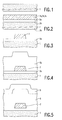
- a first embodiment of the invention will be described with reference to Figs. 1 to 16.
- This method starts from a plate-shaped substrate 1 of ferrite, an NiZn ferrite in this embodiment, which is provided with two parallel substrate faces 3a and 3b by means of polishing. Polishing may be effected by means of known polishing methods, but the method described in European Patent Application no. 92201739.7 is preferably used.
- An insulation layer 5a of zirconia is formed on one of the substrate faces, in this embodiment the substrate face 3a, for example, by means of sputter-deposition.
- an adhesive layer 7a of Mo, a layer 7b of Au and an adhesive layer 7c of Mo are successively deposited on the layer 5a by means of, for example sputtering for forming a test and/or bias winding 7.
- a photoresist layer is provided by means of, for example spin coating on the joint layers 7a, 7b, 7c. This layer is dried and subsequently exposed, using a suitable photomask. Subsequently the exposed photoresist is developed and then removed by rinsing in water.
- the layer 7c of Mo is etched whereafter the unexposed photoresist is removed by means of acetone and the layer 7b of Au is processed by means of sputter-etching with an Mo pattern as a mask.
- the winding 7 is obtained by subsequent etching of the Mo layer 7c.
- An insulation layer 5b of zirconia is provided by means of, for example sputtering on the layer 5a and the winding 7 on this layer.
- the layers 5a and 5b jointly constitute a relatively thick main layer 5 of a non-magnetic material.
- the thickness of the layer 5 is 1.1 /1.m in this embodiment.
- An Mo layer 9 is provided, for example by means of sputter-deposition on the main layer 5 provided on the substrate 1 which functions as a support, whereafter Mo is removed in two areas 11 a and 11 b by means of etching. Subsequently a sputter-etching treatment takes place, with the layer 9 functioning as a mask and two recesses 15a and 15b being formed in the main layer 5.
- a layer 17 of a soft-magnetic material is provided on the main layer 5 thus structured, and the recesses 15a and 15b are completely filled up for forming two flux guides 17a and 17b.
- the layer 17 is formed by sputter-deposition of an FeNbSi alloy. By heating this material after sputtering in a magnetic field, a layer is obtained which is magnetically soft and mechanically hard and wear-resistant.
- an FeNbSi alloy it is alternatively possible to use a CoZrNb alloy, an FeSiAI alloy or an NiFe alloy.
- the main layer provided with the filled recesses 15a and 15b is mechanochemically polished for forming a substantially perfectly plane and smooth main surface 19, part of which is formed by the insulation material of the main layer 5 and another part of which is formed by the soft-magnetic material of the flux guides 17a and 17b.
- Mechanochemical polishing which is also referred to in literature as tribo-chemical polishing, is realised in this embodiment with a colloidal suspension of Si0 2 particles in an alkali solution.
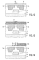
- a thin spacer layer 21 of a non-magnetic, electrically insulating material is provided on the plane, defectless main surface 19 obtained in the manner described above.
- zirconia is sputtered for this purpose.
- a layer 23a of a magnetoresistive material is provided on the layer 21, for which purpose an alloy of NiFe is sputtered in this embodiment.
- the layer 23a is subsequently structured by means of a photoresist mask and etching to form an MR element 23.
- a layer 25a of an electrically conducting material, for example Au is provided on the MR element 23, which layer is structured by means of a photoresist mask and etching to form equipotential strips 25 of a barber- pole structure and to form electrically conducting strips 25b for electrically connecting the MR element to a measuring device (not shown).
- an insulation layer 27 of, for example zirconia is provided by means of, for example sputter-deposition.
- Apertures 29 extending as far as the conducting strips 25b are etched in this insulation layer in order to provide electrical connections, whereafter a protective counterblock 31 of, for example BaTi0 3 or CaTi0 3 is secured by means of, for example an adhesive.
- the layer 27 may be planed to a desired thickness in advance, for example by mechanical polishing or lapping.
- the unit now obtained is provided with a head face 33 for cooperation with a magnetic recording medium, particularly a magnetic tape by means of operations such as grinding and/or lapping.
- the soft-magnetic material of the flux guides 17a and 17b in the thin-film magnetic head according to the invention shown in Fig. 16 is replaced by a soft-magnetic material which does not conduct electrically or has a poor electrical conductance, particularly an MnZn ferrite, an NiZn ferrite or Fe 2 0 3 ferrite, the MR element 23 may be directly provided on the main surface 19. Consequently, the insulation layer 21 may be dispensed with and the MR element 23 may be in direct magnetical contact with the flux guides 17a and 17b.
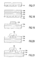
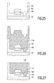
- FIG. 17 A second embodiment of the method according to the invention will be described with reference to Figs. 17 to 28.
- This method starts from a plate-shaped body 101, preferably of ferrite which is polished on both sides for forming two parallel body faces 102a and 102b.
- An insulation layer 104a of quartz is provided by means of, for example PE CVD on one of the body faces, in this embodiment the face 102b.
- An electrically conducting layer 106a of, for example mainly Au is provided on the layer 104a.
- This layer 106a is structured by means of known techniques to form an inductive transducing element or winding 106.
- quartz is deposited for forming an insulation layer 104b and an aperture 108 is etched in the two insulation layers 104a and 104b.
- a relatively thick insulation layer 104c of quartz is provided.
- the layers 104a, 104b and 104c jointly constitute a base layer 104 of a non-magnetic material.
- a layer 110 of a mask material, for example Mo is provided on the base layer 104 provided on the body 101 functioning as a base, with which mask material layer an aperture 112 is formed in the base layer 104.
- a photoresist is first deposited and structured on the layer 110, whereafter apertures 112 are formed in the layer 110 by means of etching for forming a mask.
- the base layer 104 is sputter- etched with the structured layer 110 as a mask for forming the aperture 102.
- a layer 114a of a soft-magnetic material, for example a CoZrNb alloy is provided on the base layer 104 thus structured, while the aperture 102 is completely filled up.
- the layer 114a is used for forming a flux-guiding element 114.
- the base layer 104 provided with the filled aperture 102 is subsequently mechanochemically polished by means of a colloidal suspension of Si0 2 particles in a KOH or NaOH solution to which diamond particles having an average particle size of less than 1.0 /1.m are added for creating a plane base surface 116 which is free from scratches.
- the concentration of diamond particles in said solution is less than 1 g per litre.
- the assembly thus formed from the body 101, the base layer 104 and the inductive transducing element 106 is used as a support for a main layer 105 of a non-magnetic material.
- Flux guides 117a and 117b are provided in the main layer 105 in a manner analogous to that described with reference to the first embodiment of the method according to the invention.
- a main surface 119 is also formed by means of mechanochemical polishing, whereafter an MR element 123 is provided.
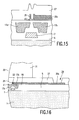
- a thin-film magnetic head manufactured by means of the second embodiment of the method according to the invention is shown in Fig. 29.
- the magnetic head has a head face 118 and comprises a body 101 serving as a base on which a non-magnetic base layer 104 is provided.
- the base layer 104 accommodates a winding 106 serving as an inductive transducing element and a flux-guiding element 114 of a soft-magnetic material terminating in the head face 118.
- a non-magnetic main layer 105 accommodating a rear flux guide 117a and a front flux guide 117b terminating in the head face 118 is provided on a mechanochemically polished base surface 116. Both flux guides are formed from a soft-magnetic material.
- a bias winding 107 may extend in the main layer 105.
- the main layer 105 has a mechanochemically polished main surface 119 on which - with a thin insulation layer being interpositioned - an MR element 123 is provided directly or indirectly.
- the invention is of course not limited to the embodiments shown.
- the soft-magnetic layer 114a by means of etching so as to form the flux-guiding element 114.
Abstract
Description
- The invention relates to a method of manufacturing a thin-film magnetic head comprising a magnetoresistive element and at least one flux guide, which method starts from a support.
- Methods of manufacturing thin-film magnetic heads are known, inter alia from EP-A 0 516 022 (herewith incorporated by reference). The magnetic heads obtained by means of the methods described in EP-A 0 516-022 are integrated magnetic heads having a contact face and comprising an inductive part and a magnetoresistive part.
- In accordance with a first method known from EP-A 0 516 022 a first structured insulation layer of Si02 is formed on a magnetic substrate of a ferrite by means of a lithographic method, which layer is subsequently provided with a layer of Au for forming a write coil. Subsequently, a second structured insulation layer is provided on which a core layer of an amorphous material based on Co is deposited. This core layer is in contact with the magnetic substrate via apertures in the insulation layers. The parts of the second insulation layer not coated by the core layer are filled up by means of a filling layer of A1203. After the filling layer has been formed, the core layer and the filling layer are planed by means of lapping. A third structured insulation layer of Si02 is deposited on the surface thus obtained on which subsequently a bias winding of Au is formed. A fourth structured insulation layer of Si02 is provided on this winding. Subsequently, a magnetoresistive element of permalloy is formed on this insulation layer. Then a fifth structured insulation layer of Si02 is provided and subsequently a yoke of an amorphous material which is based on Co and is in contact with the core layer via apertures in the three last-mentioned insulation layers.
- In accordance with a second method known from EP-A 0 516 022 two flux guides of a Co- based amorphous material are provided on a non-magnetic substrate, while an aperture between the two flux guides is filled with a first insulation layer of Si02. The surface formed by the flux guides and the first insulation layer is provided with a second structured insulation layer on which subsequently a magnetoresistive (MR) element is formed. The MR element is then coated with a third structured insulation layer on which subsequently a bias winding is formed. A fourth structured insulation layer is provided for the purpose of coating the bias winding. Subsequently a magnetic core layer of a Co- based material is formed which is in contact with one of the flux guides via apertures in the three last-mentioned insulation layers. The areas not coated by the first core layer are filled up with a filling layer of AI20a, whereafter a surface on which an inductive head part is formed is obtained by lapping.
- In the methods known from EP-A 0 516 022 the MR element is formed on an insulation layer which is provided on a lapping-processed surface. However, it has been found that such a surface extending on two or more adjacent layers of different material has unevennesses. Moreover, damage particularly in the form of scratches in and disturbances of material under the surface obtained are caused by lapping. Such a surface is inadmissible, inefficient for information transfer and may increase the risk of instabilities in the MR element provided on said surface.
- The magnetic heads obtained by the methods known from EP-A 0 516 022 have the further drawback that due to the presence of irregularities on the surface engaging the MR element, a relatively thick insulation layer is required between the MR element and the electrically conducting flux guides so as to ensure a reliable electrical insulation between the MR element and the flux guides. However, such insulation layers have a further negative influence on the efficiency of the magnetic heads. For various reasons, damage in and material disturbance under a surface above which the MR element is present are thus undesirable.
- It is an object of the invention to provide a method of manufacturing a thin-film magnetic head having a magnetoresistive element and at least one flux guide, in which the magnetoresistive element is provided on a surface which is accurately defined as regards planeness and structure.
- The method according to the invention is therefore characterized in that a main layer of a non-magnetic material is formed on the support, which layer is provided with a recess by removing material from a side remote from the support, said recess being subsequently filled up with a soft-magnetic material for forming the flux guide, whereafter the main layer provided with the filled recess is mechanochemically polished for forming a main surface at which subsequently a layer of a magnetoresistive material is provided for forming the magnetoresistive element.
- In the method according to the invention the magnetic flux guide is provided in the main layer which itself is non-magnetic. Consequently, the mechanochemical polishing operation is performed on soft-magnetic material as well as on non-magnetic material. It has surprisingly been found that despite the different material properties between the soft-magnetic and the non-magnetic material the mechanochemical polishing operation yields a very plane and smooth main surface without the materials themselves being subject to structural changes. In the method according to the invention a polished, plane surface which is free from damage is obtained for the purpose of providing the magnetoresistive element (MR element) in an electrically insulated manner, which results in a magnetic head having a stable MR element and an efficiency which is improved with respect to that of the known magnetic heads.
- Nucleation of domain walls or formation of small areas having an unwanted direction of magnetization and unwanted, sudden changes of magnetization during the read process are obviated as much as possible in a magnetoresistive element which is free from defects.
- It is to be noted that mechanochemical polishing is performed with the aid of a working surface of a polishing tool which is urged against and moved across the surface to be polished. The working surface is provided with a liquid mechanochemical polishing agent. This is an agent with which chemical and mechanical polishing is simultaneously possible. It is further to be noted that polishing without damage can be realised by purely chemical polishing. This method has drawbacks. The geometrical control, i.e. the planeness of the surface is far from optimal and many chemical polishing agents are more or less toxic and aggressive and should consequently be used in an extremely protected environment, which is a drawback in mass production. The mechanochemical polishing operation, in which components mechanically removed from the surface to be polished are chemically dissolved, leads to a very smooth and plane polished surface which is free from damage. It has surprisingly been found that if one of the components to be polished is very hard, the mechanical aspect of mechanochemically polishing will be enhanced by adding a small quantity of hard, adequate grains to the polishing agent of the mechanochemical type. Thus, even when very hard materials are used in the manufacture of heads, a smooth and plane surface which is free from damage can be realised.
- An embodiment of the method according to the invention is characterized in that a plate-shaped substrate is used as a support which is provided with two parallel substrate faces by means of mechanical and/or mechanochemical polishing, whereafter the main layer is formed on one of these faces. The other face is used as a reference face in the further process steps.
- The parallel substrate faces may be obtained by starting from a substrate having two substrate faces, the substrate faces being first prepared by means of polishing until they have a convex, plane or concave initial shape, whereafter a removal cycle is run through at least once, during which the substrate faces of a substrate whose edges are thicker than a central piece surrounded by the edges are polished in such a way that the edges successively acquire a substantially equal thickness, a smaller thickness and again a substantially equal thickness as the central piece, and during which cycle the substrate faces of a substrate whose edges are thinner than a central piece surrounded by the edges are polished in such a way that the edges successively acquire a substantially equal thickness, a larger thickness and again a substantially equal thickness as the central piece. The above-mentioned method of manufacturing parallel faces is described extensively in European Patent Application 92201739.7 (PHN 14.081 EP-P; herewith incorporated by reference).
- Substrates having parallel substrate faces have the great advantage that they can be used in a mass manufacturing process for the further steps of the method. Consequently, mechanochemical polishing steps can be performed at a later stage for the purpose of smoothing and planing a layer having a single or multiple material structure and for stop-polishing a layer having a multiple material structure, but of which only one or some materials of the layer can be polished via the mechanochemical polishing process and the other material cannot be polished.
- An embodiment of the method is characterized in that the support is formed from a soft-magnetic material, particularly a ferrite.
- It is to be noted that a ferrite is understood to be a magnetic material of, for example one of the following crystallographic groups: garnets, spinels, perovskites. Favourable properties of ferrite are its great wear resistance and its satisfactory shielding effect against disturbing fields. The stability of the magnetoresistive head is usually also favourably influenced by the effect of the ferrite on the thin-film flux guide or flux guides and the magnetoresistive element. Moreover, a ferrite support has the technological advantage that the support can be used as a flux-guiding layer.
- An embodiment is characterized in that the support is formed from an assembly which is built up from a base, a base layer of a non-magnetic material provided on the base, with an inductive transducing element and a flux-guiding element being present in the base layer, whereafter the assembly is mechanochemically polished to form a base surface for providing the main layer. The base layer may be provided with an aperture by removal of material from a side remote from the base, which aperture is subsequently filled up with a soft-magnetic material for forming the flux-guiding element. This method yields a magnetic head having a write function as well as a read function. During the method a write portion and subsequently a read portion is formed. In order to ensure an accurately defined main surface, the base layer serving as a sub-layer for the main layer is also mechanochemically polished in this embodiment. A magnetical advantage on making a planar write portion cannot be achieved. However, planarity is necessary to obtain the planar read portion having the previously mentioned advantages. Preferably the aperture in the base layer is provided by means of etching.
- An embodiment is characterized in that a plate-shaped body is used as a base, which body is provided with two parallel body faces by means of mechanical and/or mechanochemical polishing, whereafter the base layer is formed on one of these faces. The parallel body faces may be obtained by means of the method described in European Patent Application no. 92201739.7. Also in this case substrates with parallel substrate faces have advantages as far as mass manufacture, mechanochemical polishing of single materials, mechanochemical polishing of distributed materials and mechanochemical stop-polishing are concerned.
- An embodiment is characterized in that the base is formed from a magnetic material, particularly a ferrite.
- An embodiment is characterized in that the main layer is formed from zirconia. Zirconia is a crystalline material in a cubic form. The main constituent is Zr02 to which 5-10 at.% of CaO or Y203 are added. Zirconia, which may be provided, for example by sputtering, is a mechanically hard and wear-resistant material. With all soft-magnetic materials to be further described, zirconia forms a substantially perfect main surface after mechanochemical polishing. This is probably due to the great hardness of zirconia.
- From a polishing-technical point of view, zirconia is an eminently suitable material for use as a stopper layer in a mechanochemical polishing step. Since the thickness of zirconia layers can be realised with nanometer precision, plane layers of the thin-film magnetic head can be made with the same precision. Zirconia is, however, slowly etchable.
- An embodiment is characterized in that the main layer is formed from quartz. Quartz may be provided, for example by means of PE CVD. It has been found that the soft-magnetic material of the flux guide has hardly any influence on the eminent result of the mechanochemical polishing process, notably in so far as the surface is plane and free from damage, provided that there is a good adhesion between the soft-magnetic material and the quartz.
- It is to be noted that, as compared with zirconia, the much softer quartz can be subjected to a similar polishing treatment when the mechanochemical polishing process is optimized. Although the polishing process is more critical and accuracy of size is difficult to achieve, quartz has the advantage that it can be etched easily and relatively rapidly.
- An embodiment is characterized in that the recess in the main layer is formed by means of etching. The etching operation is critical because the result of the etching operation defines the non-magnetic gap which is characteristic of the read portion. Reproducibility is the paramount requirement imposed on the etching operation. Therefore, sputter-etching and reactive ion etching and, to a lesser extent, plasma etching and wet-chemical etching are preferred.
- An embodiment is characterized in that a spacer layer of a non-magnetic electrically insulating material, on which the layer of a magnetoresistive material is provided, is formed on the main surface obtained by means of mechanochemical polishing. This embodiment is particularly important if use is made of electrically conducting soft-magnetic materials for forming the flux guide. In that case an insulating spacer layer is necessary in order to prevent electrical contact between the flux guide and the MR element. A drawback of a magnetic head having a spacer layer between the MR element and the flux guide is, however, that due to the distance between the MR element and the flux guide caused by the thickness of the layer only a portion of the magnetic flux originating during operation from a magnetic recording medium is passed through the MR element. Consequently, for reasons of efficiency, it is of essential importance that such a layer can be made as thin as possible. Since the thickness of the spacer layer is determined to a considerable extent by the quality of the main surface, this spacer layer may be perfectly smooth and have no variations in thickness when the method according to the invention is used, and moreover it may be very thin, for example 0.2 /1.m with respect to the layer thicknesses of at least 0.6 /1.m required in the known magnetic heads, without any risk of short-circuit of the MR element.
- An embodiment is characterized in that an alloy from the group of alloys formed by CoZrNb alloys, FeNbSi alloys, FeSiAI alloys and NiFe alloys is used as a soft-magnetic material. These materials may be provided by means of known techniques such as sputtering or vapour deposition.
- An embodiment is characterized in that a ferrite is used as a soft-magnetic material. A ferrite usually has such a high resistivity that the MR element can be directly provided on the flux guide formed from such a material without resulting in any noticeable loss of sensitivity of the magnetic head. In other words, when ferrite is used, in which MnZn ferrite and NiZn ferrite are preferred, the spacer layer may be omitted in the method according to the invention and the layer of a magnetoresistive material may thus be directly provided on the main surface for forming the MR element. Consequently, v V a direct magnetic coupling between the MR element and the flux guide is possible. Such a coupling results in a high efficiency of the magnetic head obtained. Ferrites can be provided by means of known techniques such as sputtering, MO-CVD or laser ablation.
- The magnetic head obtained by means of the method according to the invention is provided with a head face for cooperation with a magnetic recording medium, particularly a magnetic tape or disc, while the flux guide terminates in the head face. In this connection a ferrite flux guide has the advantage that the ferrite contributes to the corrosion resistance and the wear resistance of the head face.
- An embodiment is characterized in that an NiFe alloy is used as a magnetoresistive material. The NiFe alloy can be provided by means of known techniques such as sputter-deposition or vapour deposition. The MR element formed from NiFe is provided with contact faces for realising an electrical connection with a read device. Preferably, equipotential strips having a satisfactory electrical conductivity are provided on the NiFe layer formed so as to linearize the behaviour of the MR element. This measure is described in US 4,052,748 (herewith incorporated by reference).
- An embodiment is characterized in that the base layer is formed from zirconia. In this respect zirconia is a satisfactory polish stopper material in the mechanochemical polishing process. A drawback of zirconia is that it is slowly etchable, but an important advantage is that accuracy of size is optimally achievable.
- An embodiment is characterized in that the base layer is formed from quartz. Quartz is not such a good polish stopper material in the mechanochemical polishing process as compared with zirconia, while a subtler accuracy of size should be achieved. However, an advantage is that it can be satisfactorily provided and is easily etchable.
- An embodiment is characterized in that the mechanochemical polishing treatment is performed with a colloidal suspension of Si02 particles in an alkali solution, particularly a KOH or NaOH solution. A colloidal suspension of Si02 nano particles may be used for this purpose, having, for example an average grain size of 30 nm and a pH of approximately 10 in a NaOH or KOH solution.
- It is to be noted that mechanochemical polishing is known per se from IBM Technical Disclosure Bulletin,
vol 27, no. 8, January 1985. This publication describes mechanochemical polishing of a glass structure. It is also known per se to use an agent commercially available under the trade name Syton for the mechanochemical polishing process. - An embodiment is characterized in that the mechanochemical polishing treatment is performed with a mechanochemical polishing agent comprising a colloidal Si02 solution in which grains are present which have an average particle size of less than 1.0 micrometer and a hardness which is better than the hardness of Si02. With this method according to the invention the main layer can be provided with a very smooth mechanochemically polished surface. It has been found that a surface roughness R(rms) of the polished surface smaller than 1 nm can be achieved. Measurements have shown that the material structure of the mechanochemically polished surface is not damaged. The above also applies to mechanochemical polishing of the substrate and the base layer.
- The exact effect of the above-mentioned mechanochemical polishing agent is not known. It is assumed that, in solution, the grains are enveloped by Si02 nano particles due to electrostatic forces, which enveloped particles chemically and mechanically attack the surface to be polished, while chemically attacked parts of the surface to be polished are relatively easily removed under mechanical pressure.
- Experiments have proved that optimum polishing results are achieved at an average particle size of less than 1.0 /1.m. It is therefore preferred to use grains whose average particle size is less than 1.0 micrometer, for example 100 nanometer. It is also preferred that the concentration of the grains in the colloidal solution is less than 1 g per litre. This solution is preferably alkaline and is, for example a KOH or NaOH solution.
- A1203 or zirconia is suitable as a material for the grains, but diamond is preferred because the materials are to be polished. A colloidal Si02 solution provided with diamond grains having an average particle size of less than 1.0 /1.m is therefore preferred as a polishing agent.
- The invention also relates to a thin-film magnetic head obtained by means of the method according to the invention and having a head face for cooperation with a magnetic recording medium. The magnetic head according to the invention is characterized in that the flux guide of a soft-magnetic material extends in the main layer of a non-magnetic material. In this magnetic head the magnetoresistive element has a very plane, accurately defined base, so that the magnetical stability of the magnetoresistive element is ensured. Due to the applied method according to the invention, corrosion-resistant and/or wear-resistant materials may be used for layers terminating in the head face, so that a long lifetime of the head face, hence of the complete magnetic head, is possible.
- A practical embodiment of the magnetic head according to the invention is characterized in that a further flux guide of a soft-magnetic material spaced apart from said flux guide extends in the main layer of a non-magnetic material, one of the flux guides terminating in the head face and a spacing being bridged by the magnetoresistive element located opposite the mechanochemically polished main layer.
- The invention also relates to a thin-film magnetic head having a head face and being obtainable by means of the method according to the invention, which magnetic head is characterized in that a support is provided on which a main layer of a non-magnetic material extends, which main layer has at least one recess accommodating a flux guide of a soft-magnetic material at a side remote from the support, the main layer and the flux guide at said side constituting a main surface obtained by means of mechanochemical polishing, which main surface is provided with a magnetoresistive element. The main surface, which is obtained by means of a mechanochemical polishing process, can be considered to be completely plane and free from damage. A substrate, preferably a ferrite substrate, or an assembly provided with an inductive element may be used as a support.
- These and other aspects of the invention will be apparent from and elucidated with reference to the embodiments described hereinafter.
- In the drawings
- Figs. 1 to 15 show various steps of a first embodiment of the method according to the invention,
- Fig. 16 shows a thin-film magnetic head according to the invention manufactured by means of the first embodiment of the method according to the invention,
- Figs. 17 to 28 show various steps of a second embodiment of the method according to the invention, and
- Fig. 29 shows a thin-film magnetic head according to the invention manufactured by means of the second embodiment of the method according to the invention.
- A first embodiment of the invention will be described with reference to Figs. 1 to 16. This method starts from a plate-shaped
substrate 1 of ferrite, an NiZn ferrite in this embodiment, which is provided with two parallel substrate faces 3a and 3b by means of polishing. Polishing may be effected by means of known polishing methods, but the method described in European Patent Application no. 92201739.7 is preferably used. Aninsulation layer 5a of zirconia is formed on one of the substrate faces, in this embodiment thesubstrate face 3a, for example, by means of sputter-deposition. Subsequently, anadhesive layer 7a of Mo, alayer 7b of Au and anadhesive layer 7c of Mo are successively deposited on thelayer 5a by means of, for example sputtering for forming a test and/or bias winding 7. A photoresist layer is provided by means of, for example spin coating on thejoint layers layer 7c of Mo is etched whereafter the unexposed photoresist is removed by means of acetone and thelayer 7b of Au is processed by means of sputter-etching with an Mo pattern as a mask. The winding 7 is obtained by subsequent etching of theMo layer 7c. - An
insulation layer 5b of zirconia is provided by means of, for example sputtering on thelayer 5a and the winding 7 on this layer. Thelayers main layer 5 of a non-magnetic material. The thickness of thelayer 5 is 1.1 /1.m in this embodiment. AnMo layer 9 is provided, for example by means of sputter-deposition on themain layer 5 provided on thesubstrate 1 which functions as a support, whereafter Mo is removed in twoareas layer 9 functioning as a mask and tworecesses main layer 5. After sputter-etching the remaining parts of thelayer 9 are removed, for example by wet-chemical etching. Alayer 17 of a soft-magnetic material is provided on themain layer 5 thus structured, and therecesses layer 17 is formed by sputter-deposition of an FeNbSi alloy. By heating this material after sputtering in a magnetic field, a layer is obtained which is magnetically soft and mechanically hard and wear-resistant. Instead of an FeNbSi alloy, it is alternatively possible to use a CoZrNb alloy, an FeSiAI alloy or an NiFe alloy. The main layer provided with the filled recesses 15a and 15b is mechanochemically polished for forming a substantially perfectly plane and smoothmain surface 19, part of which is formed by the insulation material of themain layer 5 and another part of which is formed by the soft-magnetic material of the flux guides 17a and 17b. - Mechanochemical polishing, which is also referred to in literature as tribo-chemical polishing, is realised in this embodiment with a colloidal suspension of Si02 particles in an alkali solution.
- A
thin spacer layer 21 of a non-magnetic, electrically insulating material is provided on the plane, defectlessmain surface 19 obtained in the manner described above. In this embodiment zirconia is sputtered for this purpose. Alayer 23a of a magnetoresistive material is provided on thelayer 21, for which purpose an alloy of NiFe is sputtered in this embodiment. Thelayer 23a is subsequently structured by means of a photoresist mask and etching to form anMR element 23. Alayer 25a of an electrically conducting material, for example Au is provided on theMR element 23, which layer is structured by means of a photoresist mask and etching to formequipotential strips 25 of a barber- pole structure and to form electrically conductingstrips 25b for electrically connecting the MR element to a measuring device (not shown). Subsequently aninsulation layer 27 of, for example zirconia is provided by means of, for example sputter-deposition.Apertures 29 extending as far as the conducting strips 25b are etched in this insulation layer in order to provide electrical connections, whereafter aprotective counterblock 31 of, for example BaTi03 or CaTi03 is secured by means of, for example an adhesive. Thelayer 27 may be planed to a desired thickness in advance, for example by mechanical polishing or lapping. The unit now obtained is provided with ahead face 33 for cooperation with a magnetic recording medium, particularly a magnetic tape by means of operations such as grinding and/or lapping. - If the soft-magnetic material of the flux guides 17a and 17b in the thin-film magnetic head according to the invention shown in Fig. 16 is replaced by a soft-magnetic material which does not conduct electrically or has a poor electrical conductance, particularly an MnZn ferrite, an NiZn ferrite or Fe203 ferrite, the
MR element 23 may be directly provided on themain surface 19. Consequently, theinsulation layer 21 may be dispensed with and theMR element 23 may be in direct magnetical contact with the flux guides 17a and 17b. - A second embodiment of the method according to the invention will be described with reference to Figs. 17 to 28. This method starts from a plate-shaped
body 101, preferably of ferrite which is polished on both sides for forming two parallel body faces 102a and 102b. Aninsulation layer 104a of quartz is provided by means of, for example PE CVD on one of the body faces, in this embodiment theface 102b. An electrically conductinglayer 106a of, for example mainly Au is provided on thelayer 104a. Thislayer 106a is structured by means of known techniques to form an inductive transducing element or winding 106. Subsequently quartz is deposited for forming aninsulation layer 104b and anaperture 108 is etched in the twoinsulation layers thick insulation layer 104c of quartz is provided. Thelayers base layer 104 of a non-magnetic material. Alayer 110 of a mask material, for example Mo is provided on thebase layer 104 provided on thebody 101 functioning as a base, with which mask material layer anaperture 112 is formed in thebase layer 104. To this end, a photoresist is first deposited and structured on thelayer 110, whereafterapertures 112 are formed in thelayer 110 by means of etching for forming a mask. Subsequently, thebase layer 104 is sputter- etched with thestructured layer 110 as a mask for forming theaperture 102. After sputter-etching the remaining parts of thelayer 110 are removed by wet-chemical etching. Alayer 114a of a soft-magnetic material, for example a CoZrNb alloy is provided on thebase layer 104 thus structured, while theaperture 102 is completely filled up. Thelayer 114a is used for forming a flux-guidingelement 114. Thebase layer 104 provided with the filledaperture 102 is subsequently mechanochemically polished by means of a colloidal suspension of Si02 particles in a KOH or NaOH solution to which diamond particles having an average particle size of less than 1.0 /1.m are added for creating aplane base surface 116 which is free from scratches. The concentration of diamond particles in said solution is less than 1 g per litre. The assembly thus formed from thebody 101, thebase layer 104 and theinductive transducing element 106 is used as a support for amain layer 105 of a non-magnetic material. - Flux guides 117a and 117b are provided in the
main layer 105 in a manner analogous to that described with reference to the first embodiment of the method according to the invention. In this method amain surface 119 is also formed by means of mechanochemical polishing, whereafter anMR element 123 is provided. - A thin-film magnetic head manufactured by means of the second embodiment of the method according to the invention is shown in Fig. 29. The magnetic head has a
head face 118 and comprises abody 101 serving as a base on which anon-magnetic base layer 104 is provided. Thebase layer 104 accommodates a winding 106 serving as an inductive transducing element and a flux-guidingelement 114 of a soft-magnetic material terminating in thehead face 118. A non-magneticmain layer 105 accommodating arear flux guide 117a and afront flux guide 117b terminating in thehead face 118 is provided on a mechanochemicallypolished base surface 116. Both flux guides are formed from a soft-magnetic material. If desired, a bias winding 107 may extend in themain layer 105. Themain layer 105 has a mechanochemically polishedmain surface 119 on which - with a thin insulation layer being interpositioned - anMR element 123 is provided directly or indirectly. A protective layer, against which acounterblock 131 is secured, extends on the MR element. - It is to be noted that the invention is of course not limited to the embodiments shown. For example, within the scope of the invention it is possible to structure the soft-
magnetic layer 114a by means of etching so as to form the flux-guidingelement 114.
Claims (25)
Applications Claiming Priority (4)
| Application Number | Priority Date | Filing Date | Title |
|---|---|---|---|
| BE9300274 | 1993-03-22 | ||
| BE9300274A BE1006925A3 (en) | 1993-03-22 | 1993-03-22 | Method for constructing a thin film magnetic head and magnetic headconstructed according to the method |
| EP93200995 | 1993-04-06 | ||
| EP93200995 | 1993-04-06 |
Publications (3)
| Publication Number | Publication Date |
|---|---|
| EP0617409A2 true EP0617409A2 (en) | 1994-09-28 |
| EP0617409A3 EP0617409A3 (en) | 1996-12-27 |
| EP0617409B1 EP0617409B1 (en) | 1999-07-28 |
Family
ID=25662715
Family Applications (1)
| Application Number | Title | Priority Date | Filing Date |
|---|---|---|---|
| EP94200675A Expired - Lifetime EP0617409B1 (en) | 1993-03-22 | 1994-03-16 | Method of manufacturing a thin-film magnetic head, and magnetic head obtainable by means of said method |
Country Status (7)
| Country | Link |
|---|---|
| US (1) | US5531016A (en) |
| EP (1) | EP0617409B1 (en) |
| JP (1) | JPH076331A (en) |
| DE (1) | DE69419642T2 (en) |
| HK (1) | HK1013720A1 (en) |
| SG (1) | SG44041A1 (en) |
| TW (1) | TW255964B (en) |
Cited By (7)
| Publication number | Priority date | Publication date | Assignee | Title |
|---|---|---|---|---|
| EP0670570A2 (en) * | 1994-03-03 | 1995-09-06 | Seagate Technology International | Magnetoresistive head and method of manufacture thereof |
| EP0747887A2 (en) * | 1995-06-07 | 1996-12-11 | Seagate Technology, Inc. | Method of fabricating an inverted magnetoresistive head |
| US5890278A (en) * | 1997-04-01 | 1999-04-06 | U.S. Philips Corporation | Method of manufacturing a magnetic head having a structure of layers |
| US5973889A (en) * | 1997-02-20 | 1999-10-26 | U.S. Philips Corporation | Single-channel magnetic head with magnetoresistive element in series with electrically conducting magnetic elements |
| US6183891B1 (en) | 1996-12-18 | 2001-02-06 | Onstream, Inc. | Magnetic head and method of manufacture |
| US6718622B1 (en) | 1998-12-03 | 2004-04-13 | Koninklijke Philips Electronics N.V. | Method of forming an assembly of stacked layers |
| US6967055B2 (en) | 2002-04-19 | 2005-11-22 | Alps Electric Co., Ltd. | Thin-film magnetic head and method of forming the same |
Families Citing this family (14)
| Publication number | Priority date | Publication date | Assignee | Title |
|---|---|---|---|---|
| KR970703576A (en) * | 1995-03-24 | 1997-07-03 | 요트.게.아 롤페즈 | System comprising a magnetic head, a measuring device and a current device |
| US6747854B1 (en) | 1997-02-20 | 2004-06-08 | Koninklijke Philips Electronics N.V. | Multi-channel magnetic head with magnetoresistive elements |
| US5936801A (en) * | 1997-04-04 | 1999-08-10 | Seagate Technology, Inc. | Head slider with partially recessed magnetoresistive element |
| US5991119A (en) | 1997-11-03 | 1999-11-23 | Seagate Technology, Inc. | Proximity head slider having recessed magnetoresistive read transducer |
| US6137661A (en) * | 1998-10-19 | 2000-10-24 | Read-Rite Corporation | System for providing a magnetoresistive head having higher efficiency |
| US6554878B1 (en) | 1999-06-14 | 2003-04-29 | International Business Machines Corporation | Slurry for multi-material chemical mechanical polishing |
| US6131271A (en) * | 1999-06-25 | 2000-10-17 | International Business Machines Corporation | Method of planarizing first pole piece layer of write head by lapping without delamination of first pole piece layer from wafer substrate |
| US6433958B1 (en) * | 1999-07-27 | 2002-08-13 | Matsushita Electric Industrial Co., Ltd. | Magnetic head, method for producing the same, video recording and reproduction apparatus including the magnetic head, and video camera including the magnetic head |
| US6510030B1 (en) | 1999-08-17 | 2003-01-21 | Seagate Technology, Llc | Transducing head and method for forming a recessed shield for a transducing head |
| US6291351B1 (en) | 2000-06-28 | 2001-09-18 | International Business Machines Corporation | Endpoint detection in chemical-mechanical polishing of cloisonne structures |
| US6712985B2 (en) | 2001-07-03 | 2004-03-30 | Hitachi Global Storage Technologies | Method and apparatus for the manufacture of thin film magnetic transducers using a compliant, soft lapping process |
| US7650697B2 (en) * | 2004-06-01 | 2010-01-26 | Nidec Corporation | Methods of manufacturing fluid-dynamic-pressure bearing and spindle motor incorporating the bearing, and spindle motor and recording-disk drive incorporating the bearing |
| US20060002023A1 (en) * | 2004-06-30 | 2006-01-05 | Quang Le | Magnetic head having a deposited second magnetic shield and fabrication method therefor |
| US20060025053A1 (en) * | 2004-07-30 | 2006-02-02 | Marie-Claire Cyrille | Method for fabricating a magnetic transducer using a slurry with spherical particles for CMP-assisted photoresist lift-off |
Citations (7)
| Publication number | Priority date | Publication date | Assignee | Title |
|---|---|---|---|---|
| JPS59152521A (en) * | 1983-02-21 | 1984-08-31 | Hitachi Ltd | Magneto-resistance effect type multielement magnetic head |
| JPS60177420A (en) * | 1984-02-23 | 1985-09-11 | Nec Corp | Composite type thin film magnetic head and its production |
| JPS6292219A (en) * | 1985-10-18 | 1987-04-27 | Victor Co Of Japan Ltd | Magneto-resistance effect type thin film magnetic head |
| JPS63317915A (en) * | 1987-06-19 | 1988-12-26 | Nec Kansai Ltd | Yoke type thin film magnetic head |
| JPH01289224A (en) * | 1988-05-17 | 1989-11-21 | Sumitomo Special Metals Co Ltd | Substrate for thin-film magnetic head and manufacture thereof |
| JPH02154309A (en) * | 1988-12-07 | 1990-06-13 | Tdk Corp | Production of substrate for thin-film magnetic head |
| EP0519558A1 (en) * | 1991-06-18 | 1992-12-23 | Koninklijke Philips Electronics N.V. | Thin film read/write head without wrap-around pole effect |
Family Cites Families (5)
| Publication number | Priority date | Publication date | Assignee | Title |
|---|---|---|---|---|
| US4052748A (en) * | 1974-04-01 | 1977-10-04 | U.S. Philips Corporation | Magnetoresistive magnetic head |
| FR2604021B1 (en) * | 1986-09-17 | 1988-10-28 | Commissariat Energie Atomique | METHOD FOR PRODUCING MAGNETIC HEADS IN THIN FILMS AND WITH A PLANAR STRUCTURE AND HEAD OBTAINED BY THIS PROCESS |
| NL9000546A (en) * | 1990-03-09 | 1991-10-01 | Philips Nv | METHOD FOR MANUFACTURING A THIN-FILM MAGNETIC HEAD AND A THIN-FILM MAGNETIC HEAD MANUFACTURABLE ACCORDING TO THE METHOD |
| JPH04351706A (en) * | 1991-05-30 | 1992-12-07 | Matsushita Electric Ind Co Ltd | Composite type thin-film magnetic head |
| EP0579298B1 (en) * | 1992-06-15 | 1997-09-03 | Koninklijke Philips Electronics N.V. | Method of manufacturing a plate having a plane main surface, method of manufacturing a plate having parallel main surfaces, and device suitable for implementing said methods |
-
1994
- 1994-03-16 EP EP94200675A patent/EP0617409B1/en not_active Expired - Lifetime
- 1994-03-16 DE DE69419642T patent/DE69419642T2/en not_active Expired - Fee Related
- 1994-03-16 SG SG1996009634A patent/SG44041A1/en unknown
- 1994-03-22 JP JP6076679A patent/JPH076331A/en active Pending
- 1994-03-22 US US08/216,575 patent/US5531016A/en not_active Expired - Fee Related
- 1994-03-30 TW TW083102778A patent/TW255964B/zh active
-
1998
- 1998-12-23 HK HK98114933A patent/HK1013720A1/en not_active IP Right Cessation
Patent Citations (7)
| Publication number | Priority date | Publication date | Assignee | Title |
|---|---|---|---|---|
| JPS59152521A (en) * | 1983-02-21 | 1984-08-31 | Hitachi Ltd | Magneto-resistance effect type multielement magnetic head |
| JPS60177420A (en) * | 1984-02-23 | 1985-09-11 | Nec Corp | Composite type thin film magnetic head and its production |
| JPS6292219A (en) * | 1985-10-18 | 1987-04-27 | Victor Co Of Japan Ltd | Magneto-resistance effect type thin film magnetic head |
| JPS63317915A (en) * | 1987-06-19 | 1988-12-26 | Nec Kansai Ltd | Yoke type thin film magnetic head |
| JPH01289224A (en) * | 1988-05-17 | 1989-11-21 | Sumitomo Special Metals Co Ltd | Substrate for thin-film magnetic head and manufacture thereof |
| JPH02154309A (en) * | 1988-12-07 | 1990-06-13 | Tdk Corp | Production of substrate for thin-film magnetic head |
| EP0519558A1 (en) * | 1991-06-18 | 1992-12-23 | Koninklijke Philips Electronics N.V. | Thin film read/write head without wrap-around pole effect |
Non-Patent Citations (6)
| Title |
|---|
| PATENT ABSTRACTS OF JAPAN vol. 10, no. 26 (P-425) [2083] , 31 January 1986 & JP-A-60 177420 (NIPPON DENKI K. K.), 11 September 1985, * |
| PATENT ABSTRACTS OF JAPAN vol. 11, no. 299 (P-621) [2746] , 29 September 1987 & JP-A-62 092219 (VICTOR CO OF JAPAN LTD), 27 April 1987, * |
| PATENT ABSTRACTS OF JAPAN vol. 13, no. 159 (P-858) [3507] , 18 April 1989 & JP-A-63 317915 (NEC KANSAI LTD), 26 December 1988, * |
| PATENT ABSTRACTS OF JAPAN vol. 14, no. 070 (E-886), 8 February 1990 & JP-A-01 289224 (SUMIMOTO SPECIAL METALS CO LTD), 21 November 1989, * |
| PATENT ABSTRACTS OF JAPAN vol. 14, no. 402 (P-1099) [4345] , 30 August 1990 & JP-A-02 154309 (TDK CORP), 13 June 1990, * |
| PATENT ABSTRACTS OF JAPAN vol. 9, no. 002 (P-325), 8 January 1985 & JP-A-59 152521 (HITACHI SEISAKUSHO K. K.), 31 August 1984, * |
Cited By (12)
| Publication number | Priority date | Publication date | Assignee | Title |
|---|---|---|---|---|
| EP0670570A2 (en) * | 1994-03-03 | 1995-09-06 | Seagate Technology International | Magnetoresistive head and method of manufacture thereof |
| EP0670570A3 (en) * | 1994-03-03 | 1997-01-22 | Seagate Technology | Magnetoresistive head and method of manufacture thereof. |
| EP0747887A2 (en) * | 1995-06-07 | 1996-12-11 | Seagate Technology, Inc. | Method of fabricating an inverted magnetoresistive head |
| EP0747887A3 (en) * | 1995-06-07 | 1997-02-26 | Seagate Technology | Method of fabricating an inverted magnetoresistive head |
| US6183891B1 (en) | 1996-12-18 | 2001-02-06 | Onstream, Inc. | Magnetic head and method of manufacture |
| US5973889A (en) * | 1997-02-20 | 1999-10-26 | U.S. Philips Corporation | Single-channel magnetic head with magnetoresistive element in series with electrically conducting magnetic elements |
| US5890278A (en) * | 1997-04-01 | 1999-04-06 | U.S. Philips Corporation | Method of manufacturing a magnetic head having a structure of layers |
| US6718622B1 (en) | 1998-12-03 | 2004-04-13 | Koninklijke Philips Electronics N.V. | Method of forming an assembly of stacked layers |
| US6967055B2 (en) | 2002-04-19 | 2005-11-22 | Alps Electric Co., Ltd. | Thin-film magnetic head and method of forming the same |
| GB2387712B (en) * | 2002-04-19 | 2005-12-07 | Alps Electric Co Ltd | Thin film magnetic head and method of forming the same |
| US7083989B2 (en) | 2002-04-19 | 2006-08-01 | Alps Electric Co., Ltd. | Thin-film magnetic head and method of forming the same |
| US7178221B2 (en) | 2002-04-19 | 2007-02-20 | Alps Electric Co., Ltd. | Method of forming a thin film magnetic head |
Also Published As
| Publication number | Publication date |
|---|---|
| EP0617409B1 (en) | 1999-07-28 |
| US5531016A (en) | 1996-07-02 |
| JPH076331A (en) | 1995-01-10 |
| TW255964B (en) | 1995-09-01 |
| DE69419642T2 (en) | 2000-02-17 |
| EP0617409A3 (en) | 1996-12-27 |
| DE69419642D1 (en) | 1999-09-02 |
| SG44041A1 (en) | 1997-11-14 |
| HK1013720A1 (en) | 1999-09-03 |
Similar Documents
| Publication | Publication Date | Title |
|---|---|---|
| EP0617409B1 (en) | Method of manufacturing a thin-film magnetic head, and magnetic head obtainable by means of said method | |
| US5483735A (en) | Method of manufacturing a thin-film magnetic head | |
| EP0584707B1 (en) | Laminate and wear-resistant thin-film magnetic head assembly formed thereon | |
| KR100488034B1 (en) | Magnetic recording medium and method for fabricating a magnetic recording medium | |
| US7207100B2 (en) | Method of manufacturing a magnetic head | |
| EP0634465B1 (en) | Method of polishing a surface of copper or an alloy comprising mainly copper | |
| JPS6149488A (en) | Magnetic resistance converter | |
| US7181827B2 (en) | Method of forming magnetic layer pattern | |
| US20060025053A1 (en) | Method for fabricating a magnetic transducer using a slurry with spherical particles for CMP-assisted photoresist lift-off | |
| US5167062A (en) | Method of manufacturing magnetic write/read head and fabrication method | |
| US6673633B2 (en) | Method of forming patterned thin film and method of manufacturing thin-film magnetic head | |
| EP0617410B1 (en) | Method of manufacturing a thin-film magnetic head, and magnetic head obtainable by means of said method | |
| EP0658881B1 (en) | Method of manufacturing a thin-film magnetic head, and magnetic head manufactured by means of said method | |
| BE1006925A3 (en) | Method for constructing a thin film magnetic head and magnetic headconstructed according to the method | |
| JPH0845017A (en) | Production of magnetic head | |
| US6718622B1 (en) | Method of forming an assembly of stacked layers | |
| Wang et al. | A perpendicular contact recording head with high moment laminated FeAlN/NiFe pole tips | |
| JPH06168418A (en) | Thin film magnetic head | |
| US6183891B1 (en) | Magnetic head and method of manufacture | |
| JPH07235002A (en) | Magnetic disk device | |
| WO2000004534A1 (en) | Method of manufacturing a thin-film magnetic head | |
| JP2001176026A (en) | Yoke-type spin valve magnetic head and its manufacturing method | |
| JPH11134621A (en) | Recording and reproducing separation type head and its production | |
| JPS60103508A (en) | Vertical magnetic recording head | |
| EP1284005A1 (en) | Method of manufacturing a magnetic element |
Legal Events
| Date | Code | Title | Description |
|---|---|---|---|
| PUAI | Public reference made under article 153(3) epc to a published international application that has entered the european phase |
Free format text: ORIGINAL CODE: 0009012 |
|
| AK | Designated contracting states |
Kind code of ref document: A2 Designated state(s): DE FR GB IT |
|
| PUAL | Search report despatched |
Free format text: ORIGINAL CODE: 0009013 |
|
| AK | Designated contracting states |
Kind code of ref document: A3 Designated state(s): DE FR GB IT |
|
| 17P | Request for examination filed |
Effective date: 19970627 |
|
| 17Q | First examination report despatched |
Effective date: 19971208 |
|
| GRAG | Despatch of communication of intention to grant |
Free format text: ORIGINAL CODE: EPIDOS AGRA |
|
| RAP3 | Party data changed (applicant data changed or rights of an application transferred) |
Owner name: KONINKLIJKE PHILIPS ELECTRONICS N.V. |
|
| GRAG | Despatch of communication of intention to grant |
Free format text: ORIGINAL CODE: EPIDOS AGRA |
|
| GRAH | Despatch of communication of intention to grant a patent |
Free format text: ORIGINAL CODE: EPIDOS IGRA |
|
| GRAH | Despatch of communication of intention to grant a patent |
Free format text: ORIGINAL CODE: EPIDOS IGRA |
|
| GRAA | (expected) grant |
Free format text: ORIGINAL CODE: 0009210 |
|
| AK | Designated contracting states |
Kind code of ref document: B1 Designated state(s): DE FR GB IT |
|
| REF | Corresponds to: |
Ref document number: 69419642 Country of ref document: DE Date of ref document: 19990902 |
|
| RAP2 | Party data changed (patent owner data changed or rights of a patent transferred) |
Owner name: ONSTREAM, INC. |
|
| ITF | It: translation for a ep patent filed |
Owner name: ING. C. GREGORJ S.P.A. |
|
| ET | Fr: translation filed | ||
| PLBE | No opposition filed within time limit |
Free format text: ORIGINAL CODE: 0009261 |
|
| STAA | Information on the status of an ep patent application or granted ep patent |
Free format text: STATUS: NO OPPOSITION FILED WITHIN TIME LIMIT |
|
| 26N | No opposition filed | ||
| REG | Reference to a national code |
Ref country code: GB Ref legal event code: IF02 |
|
| PGFP | Annual fee paid to national office [announced via postgrant information from national office to epo] |
Ref country code: FR Payment date: 20030331 Year of fee payment: 10 Ref country code: DE Payment date: 20030331 Year of fee payment: 10 |
|
| PGFP | Annual fee paid to national office [announced via postgrant information from national office to epo] |
Ref country code: GB Payment date: 20030404 Year of fee payment: 10 |
|
| PG25 | Lapsed in a contracting state [announced via postgrant information from national office to epo] |
Ref country code: GB Free format text: LAPSE BECAUSE OF NON-PAYMENT OF DUE FEES Effective date: 20040316 |
|
| PG25 | Lapsed in a contracting state [announced via postgrant information from national office to epo] |
Ref country code: DE Free format text: LAPSE BECAUSE OF NON-PAYMENT OF DUE FEES Effective date: 20041001 |
|
| GBPC | Gb: european patent ceased through non-payment of renewal fee |
Effective date: 20040316 |
|
| PG25 | Lapsed in a contracting state [announced via postgrant information from national office to epo] |
Ref country code: FR Free format text: LAPSE BECAUSE OF NON-PAYMENT OF DUE FEES Effective date: 20041130 |
|
| REG | Reference to a national code |
Ref country code: FR Ref legal event code: ST |
|
| PG25 | Lapsed in a contracting state [announced via postgrant information from national office to epo] |
Ref country code: IT Free format text: LAPSE BECAUSE OF NON-PAYMENT OF DUE FEES;WARNING: LAPSES OF ITALIAN PATENTS WITH EFFECTIVE DATE BEFORE 2007 MAY HAVE OCCURRED AT ANY TIME BEFORE 2007. THE CORRECT EFFECTIVE DATE MAY BE DIFFERENT FROM THE ONE RECORDED. Effective date: 20050316 |