EP0878919A2 - Spread spectrum communication system - Google Patents
Spread spectrum communication system Download PDFInfo
- Publication number
- EP0878919A2 EP0878919A2 EP98108713A EP98108713A EP0878919A2 EP 0878919 A2 EP0878919 A2 EP 0878919A2 EP 98108713 A EP98108713 A EP 98108713A EP 98108713 A EP98108713 A EP 98108713A EP 0878919 A2 EP0878919 A2 EP 0878919A2
- Authority
- EP
- European Patent Office
- Prior art keywords
- output
- adder
- sampling
- outputs
- data
- Prior art date
- Legal status (The legal status is an assumption and is not a legal conclusion. Google has not performed a legal analysis and makes no representation as to the accuracy of the status listed.)
- Withdrawn
Links
- 238000004891 communication Methods 0.000 title claims abstract description 41
- 238000001228 spectrum Methods 0.000 title claims abstract description 19
- 230000007480 spreading Effects 0.000 claims abstract description 25
- 238000005070 sampling Methods 0.000 claims description 62
- 238000001514 detection method Methods 0.000 claims description 21
- 230000001427 coherent effect Effects 0.000 claims description 7
- 230000015654 memory Effects 0.000 claims description 7
- 230000004044 response Effects 0.000 claims description 5
- 238000010586 diagram Methods 0.000 description 28
- 102100040862 Dual specificity protein kinase CLK1 Human genes 0.000 description 18
- PCHJSUWPFVWCPO-UHFFFAOYSA-N gold Chemical group [Au] PCHJSUWPFVWCPO-UHFFFAOYSA-N 0.000 description 17
- 238000005562 fading Methods 0.000 description 10
- 101000749294 Homo sapiens Dual specificity protein kinase CLK1 Proteins 0.000 description 7
- 101150112492 SUM-1 gene Proteins 0.000 description 7
- 101150096255 SUMO1 gene Proteins 0.000 description 7
- 238000000034 method Methods 0.000 description 6
- 230000001360 synchronised effect Effects 0.000 description 6
- 101100204393 Arabidopsis thaliana SUMO2 gene Proteins 0.000 description 5
- 101100311460 Schizosaccharomyces pombe (strain 972 / ATCC 24843) sum2 gene Proteins 0.000 description 5
- 102100040844 Dual specificity protein kinase CLK2 Human genes 0.000 description 4
- 102100040858 Dual specificity protein kinase CLK4 Human genes 0.000 description 4
- 101000749291 Homo sapiens Dual specificity protein kinase CLK2 Proteins 0.000 description 4
- 101000749298 Homo sapiens Dual specificity protein kinase CLK4 Proteins 0.000 description 4
- 230000005540 biological transmission Effects 0.000 description 4
- 102100040856 Dual specificity protein kinase CLK3 Human genes 0.000 description 3
- 101000749304 Homo sapiens Dual specificity protein kinase CLK3 Proteins 0.000 description 3
- 230000008878 coupling Effects 0.000 description 3
- 238000010168 coupling process Methods 0.000 description 3
- 238000005859 coupling reaction Methods 0.000 description 3
- 102100034033 Alpha-adducin Human genes 0.000 description 2
- 102100024348 Beta-adducin Human genes 0.000 description 2
- 102100034004 Gamma-adducin Human genes 0.000 description 2
- 101000799076 Homo sapiens Alpha-adducin Proteins 0.000 description 2
- 101000689619 Homo sapiens Beta-adducin Proteins 0.000 description 2
- 101000799011 Homo sapiens Gamma-adducin Proteins 0.000 description 2
- 101000629598 Rattus norvegicus Sterol regulatory element-binding protein 1 Proteins 0.000 description 2
- 101100381996 Saccharomyces cerevisiae (strain ATCC 204508 / S288c) BRO1 gene Proteins 0.000 description 2
- 230000001413 cellular effect Effects 0.000 description 2
- 230000003247 decreasing effect Effects 0.000 description 2
- NAWXUBYGYWOOIX-SFHVURJKSA-N (2s)-2-[[4-[2-(2,4-diaminoquinazolin-6-yl)ethyl]benzoyl]amino]-4-methylidenepentanedioic acid Chemical compound C1=CC2=NC(N)=NC(N)=C2C=C1CCC1=CC=C(C(=O)N[C@@H](CC(=C)C(O)=O)C(O)=O)C=C1 NAWXUBYGYWOOIX-SFHVURJKSA-N 0.000 description 1
- 101000625226 Homo sapiens Melanoregulin Proteins 0.000 description 1
- 102100024976 Melanoregulin Human genes 0.000 description 1
- 239000000654 additive Substances 0.000 description 1
- 230000000996 additive effect Effects 0.000 description 1
- 102220414579 c.213T>C Human genes 0.000 description 1
- 230000008859 change Effects 0.000 description 1
- 230000003292 diminished effect Effects 0.000 description 1
- 238000000605 extraction Methods 0.000 description 1
- 230000006870 function Effects 0.000 description 1
- 230000010354 integration Effects 0.000 description 1
- 238000010295 mobile communication Methods 0.000 description 1
- 230000010355 oscillation Effects 0.000 description 1
- 230000002093 peripheral effect Effects 0.000 description 1
- 102220042260 rs34160178 Human genes 0.000 description 1
- 102220241019 rs527453026 Human genes 0.000 description 1
Images


Classifications
-
- H—ELECTRICITY
- H04—ELECTRIC COMMUNICATION TECHNIQUE
- H04B—TRANSMISSION
- H04B1/00—Details of transmission systems, not covered by a single one of groups H04B3/00 - H04B13/00; Details of transmission systems not characterised by the medium used for transmission
- H04B1/69—Spread spectrum techniques
- H04B1/707—Spread spectrum techniques using direct sequence modulation
- H04B1/709—Correlator structure
- H04B1/7093—Matched filter type
Definitions
- the present invention relates to a spread spectrum communication system for the mobile communication, wireless LAN etc.
- the spread spectrum communication system seems hopeful in the fields of mobile cellular radio and wireless LAN due to its frequency efficiency and confidentiality.
- DS-CDMA direct-sequence code division multiple access
- the modulated signal consists of all in-phase component (I-component) Si and a quadrature component (Q-component) Sq.
- Si IiCi-IqCq
- Q-component quadrature component
- Si IiCi-IqCq
- IiCq-IqCi an information to be transmitted is divided into I-component Ii and Q-component.
- Ci is a spreading code of an I-component and Cq is of a Q-component.
- the demodulated signal consists of an I-component Ri and a Q-component Rq.
- Ri IiCi-IqCq
- Rq IiCq-IqCi
- Di RiCi+RqCq
- Dq -RqCq+RqCi
- Di Ii(Ci 2 +Cq 2 )
- Dq Iq(Ci 2 +Cq 2 )
- the received signal is despreaded and divided into the I- and Q-components Di and Dq.
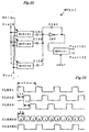
- Fig.30 shows a conventional receiver including a matched filter of the CDMA communication system.
- An analog signal Ain4 of an intermediate frequency (IF) received by the receiver, is divided into the two signal components Ri and Rq.
- the carrier signal is removed by a low-pass filter LPF, then, Rq is input to matched filters MF1 and MF2 and Ri is input to matched filters MF3 and MF4.
- the spreading code Cq for Q-component is given from a code generator PNQ to MF2 and MF3, and spreading code Ci for I-component is given from a code generator PNI to MF1 and MF4.
- Each matched filter multiplies the signal component of successive time sequence by the spreading code and sums them up.
- Fig.31 shows a conventional receiver including a sliding correlator, which converts the received signal Ain5 of the IF into I- and Q-components by the quadratic detector and LPF.
- the I- and Q-components are multiplied by Cq and Ci by four multipliers shown by X. Then, the I- and Q-components are composed by the adders similarly to the above. The result of the composition is coherently tracked and a correlation peak is detected.
- Fig.32(a) shows a frame format of transmission data of DS-CDMA communication.
- Each frame consists of one pilot symbol block P1, P2, ..., Pn and one information symbol block I1,I2, ..., In, respectively.
- Each pilot block has predetermined L symbols. L is for example "4".
- Each information block has predetermined number, for example "36", of symbols. These symbols are modulated by QPSK and spreaded by the predetermined spreading code sequence.
- a fading complex envelop is predicted from the pilot symbols and fading compensation is performed according to the envelop.
- the rake combining and coherent detection are performed.
- a frame synchronization signal is output when the pilot symbol block is of a predetermined pattern.
- Fig.32(b) shows a conventional rake receiver.
- I- and Q-component of an output of a complex matched filter 80 is input to a delay detection circuit 82, a signal level detection circuit 84 and a phase correction circuit 86.
- the first path of the multi-path is detected by the circuit 82 which output an output to a frame synchronization circuit 83 for detecting a timing of the frame synchronization.
- the timing is input to a phase correction portion 86.
- a rake combiner 87 and a data decision portion 88 are serially connected to the phase correction portion 86.
- the phase correction portion calculates a phase rotation of the pilot symbol by comparing the received pilot symbol with a predetermined pilot symbol. Then, a correction vector is calculated for compensating the phase error due to fading etc.
- the information is coded by differential coding at a transmitter.
- the delay detection is performed according only to the strongest path among multi-path, so the accuracy of the frame synchronization detection is rather low. The reliability of the received data is low.
- the present invention is invented so as to solve the conventional problems and has an object to provide a spread spectrum communication system of small circuit size, high communication capacity and low electric power consumption.
- spreading code for in-phase and quadrature components are composed by addition and subtraction and the received signal is multiplied by these composed code for despread.
- a multi-path signal is provisionally judged by one path so that phase compensation can be performed.
- the signal compensated is combined by a rake combiner and delay detected.
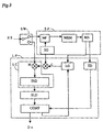
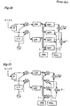
- Fig.1 shows a matched filter for the present invention.
- the matched filter has sampling and holding circuits SH1 to SHn corresponding to spreading ratio n of the matched filter MF.
- An in-phase component (I-component) Ri and a quadrature component (Q-component) Rq of a received signal are added by the first adder ADD1 and input to the sampling and holding circuits SH1 to SHn.
- the sampling and holding circuits are controlled by a control signal (not shown) so as that SH1, SH2, ..., SHn successively and circulated sample and hold successive outputs from the adder ADD1 along the time sequence. Since the data to be held by the sampling and holding circuits are not transferred between adjacent sampling and holding circuits, the transfer error of data is not occurred.
- the spreading code sequence Ci and Cq are sifted and circulated synchronously to the sampling and holding in response to a clock of chip rate.
- Outputs of the sampling and holding circuits SH1 to SHn are input to multiplication circuits M11, M21,..., Mn1 for I-component and to multiplication circuits M12, M22,..., Mn2 for Q-component.
- the PN code Ci for I-component is input to M11 to Mn1
- PN code Cq for Q-component is input to M12 to Mn2.
- Outputs from M11 to Mn1 are input to the second adder ADD2 so as to be summed up to be a total summation of I-component
- outputs from M12 to Mn2 are input to the third adder ADD3 so as to be summed up to be a total summation of Q-component.
- the outputs of the ADD2 and ADD3 are input to the fourth adder ADD4 and a subtraction circuit SUB.
- R R of the I-component Ri and Q-component Rq are given by the formula (9).
- the outputs of ADD4 and SUB are approximatel expressed as in the formulae (10) and (11).
- Cq and Ci are quasi-orthogonal to each other, that is, of low correlation to each other, the judgment whether the received signal is oriented to the receiver is possible if one of the components is not so deteriorated.
- the error correction is also possible.
- the quasi-orthogonal means "orthogonal" including a correlation of "0".
- the communication reliability is equal to a communication of two channels, however the number of sampling and holding circuits SH1 to SHn is equivalent to that of one communication channel of the conventional system. Therefore, the circuit size of thin embodiment is much smaller than that of the conventional circuit.
- the correlation between I- and Q-components cannot be neglected when the terms on the left side of the formulae (12) and (13) due to errors during communication path.
- the correlation output (electrical power) is averaged through recursive integration with respect to time for decreasing the influence of the correlation.
- Fig.2 shows a receiver applied to the communication system according to the present invention.
- the received signal Ain2 by the antenna system and a RF receiver portion is divided by a divider D into 2 signals which are converted by a quadratic detector into I- and Q-components, respectively.
- the carrier signal is removed by low-pass filters LPF1 and LPF2 from the components so that the I- and Q-components are extracted.
- the components are input to matched filter MF for approximately calculating I- and Q-components by the calculation of formulae (7) to (13) using PN code supplied from the PN generator PNG.
- the outputs from LPF1 and LPF2 are input parallelly to a plurality of sliding correlators SC1 to SCn.
- the matched filter MF is used only for the acquisition of the received signal and the sliding correlators are used for data demodulation and tracking As shown in the formulae (12) and (13), the output f the matched filter is nearly equal t the I- and Q-components, however the I- and Q-components may not be well divided due to noises.
- the sliding correlators calculate simple multiplication of the received signal RS and the PN code, ,so the components are well divided. The sliding correlators cannot perform fast acquisition because only one multiplication circuit is provided for each sliding correlator.
- the combination of the matched filter for acquisition and the sliding correlators for demodulation and for tracking realizes fast acquisition without enlarging the circuit size. The demodulation performance is high.
- the output of the matched filter is input to a power calculation portion PC for calculating the electrical power of the output.
- the calculation result is recursively integrated by a path-detector PD for selecting predetermined number of signal paths of higher levels. These paths occurs due to reflections etc. during the communication path.
- An output of PD is input to correlation controller CC for controlling the sliding correlators SC1 to SCn so that the sliding correlators are synchronized with the selected paths.
- the synchronized signals are demodulated by the sliding correlators and outputs from them are combined by a rake combiner RAKE.
- Do in Fig.2 is an output after the rake combining.
- Fg.3 shows a receiver for two-stage rapid acquisition method proposed in "Two-Stages Rapid Long Code Acquisition Scheme in DS-CDMA Asynchronous Cellular System", Kennichi Higuchi, the TECHNICAL REPORT OF IEICE, CS96-19, RCS96-12(1996-05).
- a common short code for every base stations and proper short codes for the base stations different from one another are defined, and two steps demodulation of these short codes is performed when the control channel is transmitted.
- the control channel is transmitted every predetermined periods with two-stages spreading modulation.
- a timing of a long code is detected from the demodulated signal by the short codes. The acquisition of the long code becomes faster.
- RS through the divider and the low-pass filter is input to a switch SW for selectively outputting the signal into two outputs.
- the first output is input to a short code processor SP and the second is input to a long code processor LP.
- the SP includes the matched filter MF and a short code generator SG for inputting the short code into MF.
- the SP calculates correlation of RS and the shot code so as to detects the long code timing for initial cell search and peripheral cell search.
- the LP includes the sliding correlators and a long code generator LG for inputting the long code into the sliding correlators.
- the LP calculates correlation of RS and a combined code of the short codes and the long code so as to demodulate the signal.
- the output of MF is input to a memory MEM for registering a plurality of electrical power levels.
- a maximum extraction portion MS is connected to MEM for selecting the maximum of the power.
- An output of MS is input to LG.
- MS generates a timing of the correlation calculation between RS and the long code y SC, that is, a timing of generating of the long code.
- the short code is combined with the long code by an exclusive-or gate G.
- the combined code is input to a multiplier M. Then, the two-stages demodulation is completed and tile long code synchronization is established.
- an output of the multiplier is input to an integrator IND for integrating the multiplication result.
- a square-law detector SLD is connected to an output IND and a comparator CMP is connected to an output of SLD.
- a threshold determining circuit TD is connected to an output of MS so that COMP compares the output of SLD with an output of TD.
- the correlation of the signal with the short code is converted into the power which is compared with a threshold determined by TD. Since TD determines the threshold from the power detection in SP, an appropriate threshold is obtained.
- the long code synchronization signal Do is appropriate.
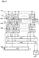
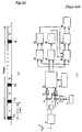
- Fig.4 is a block diagram of the next embodiment of the present invention of a multi-path of four paths. This embodiment is applicable to other numbers of multi-path.
- a signal input portion 1 to which I- and Q-components output from a matched filter are input.
- the multi-path signal consists of signals r1, r2, r3 and r4 corresponding to the first path #1, the second path #2, the third path #3 and the fourth path #4, respectively.
- the reference 10 designates a provisional judgment portion 10 for provisionally judging the transmission symbol of r1, 21 designates the first phase correction means for r1, 22 designates the second phase correction means for r2, 23 designates the third phase correction means for r3, and 24 designates the fourth phase correction means for r4.
- the reference 60 designates a rake combiner, 61 to 64 designate delay means for giving predetermined delay time to outputs of the phase correction means 21 to 24.
- 65 designates an adder for adding outputs from the delay means 61 to 64 together and for outputting the addition result at an output terminal 2.
- the phase correction means 21 includes a correction vector calculation portion 31 for calculating a correction vector M1 from a phase signal ⁇ output from the provisional judgment portion 10 and the r1.
- 41 designates a memory for delaying r1 by a time necessary for the calculation in the c
- the capacity of the memory is smaller than the conventional system.
- phase correction circuit 51 designates a phase correction circuit for performing phase correction of r1 output from the memory 41 using the correction vector M1 output from the correction vector calculation portion 31.
- An output of the phase correction circuit 51 is input to the first delay means 61.
- phase correction means 22 to 24 are similar to 21, which have correction vector calculation portions 32 to 34, memories 42 to 44 and phase correction circuits 52 to 54.
- Fig.5 shows an example of the received signal received at the terminal 1.
- a base-band signals r1, r2, r3 and r4 passed trough different paths are output from the complex matched filter.
- the signals are expressed as in the formulae (14) to (17).
- Fig.6 shows a relationship between data SISQ to be modulated and the phase ⁇ , that is, a result of the provisional judgment.
- the phase correction means 22 to 24 are similar to the means 21, so only the means 21 is described.
- the correction vector calculation portion 31 calculates M1 by multiplying r1 by a conjugate complex number of ⁇ as shown in the formula (20).
- the phase component of the correction vector M1 consists only of ⁇ 1 depending on the fading and ⁇ depending on the initial phase error ⁇ , without the phase ⁇ corresponding to the information modulation.
- the phase correction portion 51 multiples r1 by a conjugate vector M1* of M1 so as to output M1*r1.
- Other phase correction means 22 to 24 similarly outputs a corrected signal M2*r2, M3*r3 and M4*r4, respectively. These outputs are adjusted in timing in the delay circuits 61 to 64 to be synchronized and added by the adder 65.
- a combined output RKout of rake combining is obtained according to the formula (21).
- the phase of RKout is an addition of the information modulation ⁇ and the error ⁇ .
- ⁇ is substantially constant for all the symbols.
- S/N ratio is low and fading coefficient changes steeply, ⁇ changes quickly. While, ⁇ changes in response to the information.
- An output of the formula (22) is obtained by inputting RKout to a delay detection circuit.
- the delay detection output D corresponding to RKout(j-1) of (j-1)th symbol and RKout(j) of (j-1)th symbol is expressed by the formula (22).
- D RKout + ( j -1)
- RKout ( j ) DI + jDq
- ⁇ is deleted and a signal of phase difference between jth and (j-1)th symbol is output. Therefore, a delay detection signal without phase ertor can be obtained by the rake combining signal of multi-path signal.
- Fig.7 is a receiver for DS-CDMA communication using the above embodiment for improving accuracy of frame synchronization.
- the provisional judgment portion 10 is connected to a complex matched filter 80 which outputs a base-band signal corresponding to a plurality of paths.
- a multi-path selection portion 85 is connected to the matched filter 80 for selecting a predetermined number of multi-path signals of higher electric power.
- the portion 10 performs the provisional judgment corresponding to the highest path selected by the portion 85 for outputting ⁇ .
- the signal ⁇ is input to the phase correction portion 20 in which the phase correction means 21 to 24 synchronize the received signal with the phase judged by the portion 10.
- the synchronized signal is combined by the rake combiner 60.
- the rake combining output RKout is input to a delay detection circuit 82 output of which is input to a frame synchronization circuit 83.
- the circuit 83 detects matching of series of delay detection outputs with information pattern of predetermined pilot symbols so that a frame synchronization is detected.
- An output of frame synchronization is input to a coherent detection circuit 100.
- the circuit 100 receives an output of the matched filter 80 for coherent synchronization of the received signal of information symbol block according to the frame synchronization signal.
- the circuit 100 includes a phase correction portion 86, a rake combiner 87 and a data decision circuit 88.
- the frame synchronization is accurate because the rake combining output is delay detected relative to the conventional system.
- Fig.8 shows another receiver in which an output of the rake combiner 60 is parallelly output to a synchronization circuit 110 and a delay detection circuit 82. Both of the pilot symbol block and information symbol block of the received signal are input to the phase correction portion 20 and the rake combiner 60.
- the delay detection circuit 82 and the frame synchronization circuit 83 are serially connected to the rake combiner 60.
- the output of the circuit 83 is input to the coherent synchronization circuit 110.
- the output of the rake combiner 60 is input to the circuit 110 for coherent synchronization.
- the signal from the rake combiner is the combined data of multi-path signal, so the output of the circuit 110 is a data after phase correction as well as data decision.
- phase correction portion 86 included within the information symbol output from the rake combiner 60.
- the compensated signal is then judged by a data decision portion 88.
- This embodiment is smaller in circuit size than the embodiment in Fig.7.
- the differential BPSK (DBPSK) or the differential QPSK (DQPSK) is applied at the transmitter so that pilot signal is not necessary for fading compensation. The transmission efficiency is improved.
- Fig.9 shows a transmitter corresponding to the receiver in Fig.8.
- the reference 90 designates a differential coder for differential coding of the information signal, applicable to DBPSK or ⁇ /4 shift DQPSK.
- 91 designates a spreading portion for spreading I-channel of the information signal output from the coder 90
- 92 designates a spreading portion for spreading Q-channel of the information signal output from the coder 90.
- 93 designates a PN code generator for supplying a spreading code sequence to the coder 91 and 92.
- 94 designates a carrier wave oscillator
- 95 designates a ⁇ /2 phase shifter
- 96 and 97 designates multipliers
- 98 designates an adder for adding outputs from the multipliers 96 and 97.
- the outputs from the spreading portions 91 and 92 are quadrically modulated. When DBPSK is applied, only the I-channel is output from the coder 90.
- Fig.11 shows provisional judgment of DBPSK.
- I-component r1I of r1 is positive or zero, SI is judged to be “1", and when negative, SI is judged to be "0".
- the calculation of the formula (18) is performed.
- Fig.10 is a block diagram of a rake receiver in which the coherent detection circuit and frame synchronization circuit are deleted.
- a delay detection circuit 89 is connected to an output of the complex matched filter.
- An output D of the circuit 89 is judged by the circuit following to the circuit 89.
- the information bit is judged to be "0" and "1" when the real component DI of D is more and less than zero, respectively.
- Fig.12 shows the provisional judgment of ⁇ /4 shift DQPSK.
- the signal r1 is judged to be of a phase ⁇ when its phase is between ⁇ ⁇ /8.
- the correction vector is calculated similarly to the above embodiments according to ⁇ obtained as above.
- Fig.13 is a block diagram of a matched filter.
- G1 consists of a plurality of sampling and holding circuits SH11 to SH1n and G2 consists of a plurality of sampling and holding circuits SH21 to SH2n.
- An analog input voltage in is parallelly input to these sampling and holding circuits SH11 to SH1n and SH21 to SH2n.
- the sampling and holding circuit SH1i in the first group G1 corresponds to the sampling and holding circuit SH2I in the second group G2.
- the groups G1 and G2 are driven by clock signals CLK1 and CLK2 so that one of the groups is used for sampling and holding Vin successively.
- CLK1 and CLK2 are of the same cycle of a tip time and are shifted by a half of the tip time to each other. For example, SH11 to SH1n in G1 successively take Vin, then SH21 to SH2n successively take Vin. Data is not transferred between adjacent sampling and holding circuits in order to prevent transfer error of the data.
- the multi-plexer MUX1i is switched by a clock signal CLK3 so that the output is switched every half tip times from G1 to G2 or vice verse. This switching of the multi-plexers and the two groups of sampling and holding circuits enable a double sampling, that is, sampling of two sets of successive data sequence shifted by a half tip time.
- the outputs of MUX2i corresponds to "1" (shown by "+”) and "0" (shown by "-") of one PN code, respectively.
- the former outputs are connected to the first adder SUM1 and the latter outputs are connected to the second adder SUM2.
- the matched filter performs the calculation in the formula (23).
- the adders SUM1 and SUM2 sum the first and second outputs up, respectively, of multi-plexers MUX21 to MUX2n.
- the addition results are input to a subtraction circuit SUB for subtracting the total sum of the second outputs from the total sum of the first outputs.
- the switching of the multi-plexers MUX2i is controlled by PN code sequence stored in a PN register PNG.
- PNG is a shift register last stage of which is fed back to the first stage.
- the PN codes are shifted on every tip times so as to be shifted and circulated.
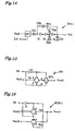
- the sampling and holding circuit SH11 is shown in Fig.14.
- An input voltage Vin2 is connected to a switch SW output of which is connected to a capacitance C21.
- Three stages MOS inverters I1 to I3 serially connected are connected to C21 at the first stage inverter I1, and an output Vo2 of the last stage inverter I3 is fed through a feedback capacitance C22 back to an input of I1.
- An inversion of Vin2 is generated at Vo2 with good linearity.
- C21 is charged by an electric charge corresponding to Vin2.
- SH11 holds S(t) in the formula (23).
- SW is controlled by a control signal S2.
- the output of the last stage inverter I3 is grounded through a grounded capacitance C23, and an output of I2 is connected through equilibrium resisters R21 and R22 to the supply voltage Vdd and the ground, respectively. Unexpected and unstable oscillation of the above circuit including the feedback loop is prevented. Since SH12 to SH1n and SH21 to SH2n are similarly, descriptions therefor are omitted.
- the switch SW is shown in Fig.15.
- a n-typc MOS transistor is connected at its source and drain to a drain and source, respectively, of a p-type MOS transistor.
- a transistor circuit T3 is given.
- An input voltage Vin3 is input to T3 at the drain of n-type MOS.
- T3 is connected at the source of n-type MOS through a dummy transistor DT3 to an output terminal Vout3.
- the control signal S3 (S2) is input to a gate of the n-type MOS, an inverted signal by an inverter I4 of S3 is input to a gate of p-type MOS.
- S3 When S3 is high level, T3 is conductive, and when S3 is low level, T3 is disconnected.
- the multi-plexer MUX11 is shown in Fig.16.
- the n-type MOS transistor is connected at its source and drain to drain and Source of the p-type MOS transistor.
- the sources of the n-type MOS transistors are commonly connected an output Vout4.
- the output (shown by Vin41) of SH11 is input to the drain of the n-type MOS in T41
- the output (shown by Vin42) of SH21 is input to the drain of the n-type MOS in T42.
- a signal S4 is input to the gate of n-type MOS transistor in T41 and to the gate of p-type MOS transistor in T42.
- An inverted signal of S4 by an inverter I5 is input to the gate of p-type MOS transistor in T41 and to the gate of n-type MOS transistor in T42.
- MUX11 alternatively outputs the output from SH11 or SH21 in response to S4. Since MUX12 to MUX1n are similar to MUX11, descriptions therefor are omitted.
- the multi-plexer MUX21 consists of a pair of multi-plexers MUX51 and MUX52 similar to MUX11.
- An output Vin51 from MUX11 and a reference voltage Vref are input to MUX51 and MUX52, respectively.
- a control signal S5 is input to MUX51 and an inverted signal of S5 by an inverter I6 is input to MUX52.
- MUX51 outputs Vin5 as an output Vout51 and MUX52 outputs Vref as an output Vout52.
- MUX52 When S5 is low level, MUX52 outputs Vin5 as an output Vout52 and MUX51 outputs Vref as an output Vout51.
- the circuit sized is diminished to be a half of the conventional matched filter because the adders SUM1 and SUM2 are commonly used for the first and second groups.
- the electrical power consumption is decreased.
- S(t-i ⁇ Tc) is a voltage held by the sampling and holding circuit and PN(i) is a PN code or signal S5 to be supplied to the sampling and holding circuit
- PN(i) is a PN code or signal S5 to be supplied to the sampling and holding circuit
- Fig.20 shows a timing of clocks CLK1 to CLK4.
- CLK1 and CLK2 are shifted by ts/2.
- CLK3 and CLK4 are synchronous to CLK1.
- CLK1 is expressed by a function CLK(t) of time t.
- the control speed of the PN register is rather slow in spite of the double sampling.
- sampling and holding circuits which are alternatively selected by the first multi-plexers.
- the control signal for the first multi-plexers Is CLKMUX and the control signal for the shift register is CLKSRG, the relationship among them is as in Fig.23.
- CLKG1, CLKG2 and CLKG3 are of the same cycle ts and successively shifted by ts/3.
- CLKMUX is of a cycle of ts/3.
- CLKSRG is identical to CLKG1.
- the sampling clock for ith sampling and holding circuit is expressed by CLK(t+i ts/m), when the number of the sampling and holding circuit is m, the sampling cycle is ts and the clock of the first sampling and holding circuit is CLK(t).
- the control signal for the first multi-plexer is used for alternatively selecting the groups in a cycle of ts/m.
- the control signal of the shift register is identical to one of the clocks for the sampling and holding circuit groups.
- the adder SUM1 is shown in Fig.18.
- SUM1 consists of a plurality of capacitances C61 to C6n corresponding to MUX21 to MUX2n.
- the first outputs (shown by Vin61 to Vin6n) of the multi-plexers are connected to the capacitances C61 to C6n, respectively.
- the outputs of these capacitances are commonly connected to an inverting amplifier output of which is connected through a feedback capacitance C6f to its input.
- the output Vout6 of the inverter is as in the formula (24).
- I61, I62 and I63 are MOS inverters, R61 and R62 are equilibrium resistances and C6g is a grounded capacitance.
- the capacitances C61 to C6n performs addition as a capacitive coupling, however, the addition can be hierarchically performed by a plurality of stages of capacitive couplings.
- the subtraction circuit SUB is shown in Fig.19.
- SUB has a capacitance C71 connected to the output (shown by V71) of SUM1 and a capacitance C74 connected to the output (shown by V72) of SUM2.
- Three inverters I71 to I73 serially connected are connected to an output of the capacitance C71.
- An output of the last stage inverter I73 is connected through a feedback capacitance C72 to an input of the inverter I71.
- An inversion of the input voltage V71 is generated at the output of I73 with good linearity.
- the output of I73 is connected to a capacitance C75 an output of which is connected together with an output of C74 to three stages inverters I74 to I76 serially connected.
- An output of the last stage inverter I76 is connected through a feedback capacitance C77 to an input of the inverter I74.
- An inversion of an output of a capacitive coupling consisting of C74 and C75 is generated at the output of I76 with good linearity.
- the output Vout7 of I76v is expressed by the formula (25).
- Vout7 Vin72-Vin71 This means that a subtraction of the summations is performed.
- the pairs of R71 and R72, and R73 and R74 are equilibrium resistances, and C73 and C77 are grounded capacitance.
- the reference voltage Vref is set to be equal to a threshold of the MOS inverters.
- the threshold is usually set to be Vdd/2.
- Vdd is a supply voltage of the MOS inverter.
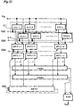
- Fig.21 shows another filter circuits. Similar portions to those of the circuit in Fig.13 is designated by the same references and the descriptions therefor are omitted.
- This filter circuit can be applied to more general usage because the multipliers are digital data of a plurality of bits.
- the multiplication circuits MUL11 to MUL1n are used instead of the multiplexers MUX21 to MU2n in Fig.13, and a multiplier register MREG is used instead of the PN register PNG.
- the multiplication circuit MUL11 has k number of capacitances C101 to C10k corresponding to k bits of multipliers. These capacitances are commonly connected at their outputs to an inverter INV consisting of three stages MOS inverters. An output of INV is connected through a feedback capacitance C10f to an input of INV. Multi-plexers MUX101 to MUX10k corresponding to C101 to C10k are connected inputs of the corresponding capacitances, respectively. Each of the multi-plexers is connected at its input to an input voltage Vin10, that is, the output of the first multi-plexer and a reference voltage. C101 to C10k have capacities corresponding to 2 0 to 2 k for binary weighting.
- Fig.24 shows one embodiment of code generating circuit used in the DS-CDMA communication system.
- the code generating circuit has a shift register 11 for generating a m-sequence.
- the Gold sequence can also be generated by the same circuit.
- the reference 11 designates a shift register of m stages from the 0 th to the (m-1)th.
- m is not less than "2".
- the shift register has serial input and serial output as well as a parallel inputs and parallel outputs.
- An adder 13 modulo "2" is connected to the serial input of the shift register 11, and a clock CLK is input to a shift-clock input terminal of the shift register.
- a m-bits data for initializing the shift register 11 is input to the parallel inputs, which data are set to the stages of the shift register by an output of a counter 15 at the initial condition.
- the references 12 1 to 12 m-1 designate multiplication circuits for multiplying data in the stages of the shift register 11 by multipliers b 1 to h m . 1 .
- Each of the multipliers hi is “1" or “0” for outputting data in the corresponding stage to the adder 13 when hi is “1” and for preventing output of data when hi is "U”.
- the adder 13 adds outputs from the multiplication circuits 12 1 to 12 m-1 and the 0 th stage of the shift register with a modulus of "2".
- the output of the adder 13 is fed back to the serial input of the shift register 11.
- the output from the 0 th stage can be deemed as multiplied by a multiplier of "1".
- a combinational logic circuit 14 is connected to the parallel outputs of the shift register 11 for addition of modulus of "2".
- the counter 15 counts CLK for initializing the data in the shift register 11 when a counted value reaches a predetermined value.
- the initial data is set also by a control signal generated by the counter 15.
- a m-sequence of a cycle of 2 m -1 is generated by the shift register of m stages, circuits 12 1 to 12 m-1 and the adder 13 according to the formula (27).
- the code is output from the serial output of the 0 th stage.
- h(X) X m +h m-1 X m-1 +...+h 1 X+1
- the m-sequence can be set in its phase by adjusting the initial condition of the shift register 11.
- the m-sequence is a characteristics that an addition modulo "2" of a code sequence and a sequence shifted with circulation of the former sequence becomes another sequence shifted with circulation of the sequence. It is called "shift additive characteristics". Any shifted m-sequence can be generated by selecting data included in the necessary sequence and by adding the data modulo "2".
- the logic circuit 14 selects the necessary data from the parallel output of the shift register 11 according to the control signal.
- the shifted code sequence can be output as soon as a m-sequence is output without delay.
- a plurality of shifted sequences can be output when a plurality of combinational logic circuits are provided.
- the shift register 11 is repeatedly initialized on counting an intermediate number of stages of the shift register.
- Fig.25 shows a simple circuit for code generation. There are three stages in the shift register and a m-sequence of a cycle of 7bits. A sequence shifted by 4bits is simultaneously generated.
- the reference 21 designates a shift register with three stages.
- 22 designates an adder modulo "2" for adding the 0 th and the second stages with modulus "2" and for inputting the addition result to the data input of the shift register.
- This calculation is equivalent to an exclusive-or calculation.
- An initializing data is input to the parallel input of the shift register at the initial condition.
- the m-sequences generated according to the primitive polynomial (28) in response to CLK impressed to the shift clock input terminal is output from the 0 th stage output OUT0.
- the reference 23 designates an adder modulo "2" for adding outputs OUT0, OUT1 and OUT3 of the 0 th , the first and the second stages.
- the adder is equivalent to the circuit 14 in Fig.24.
- An output of the adder is expressed by the formula (29).
- OUT 4 OUT 2 ⁇ OUT 1 ⁇ OUT 0 OUT4 is a shifted sequence by 4bits of OUT0.
- Fig.25(b) is a table showing outputs from the stages. At the initial condition of time “0", (1,1,0) are set in the 0 th to the second stages by the initializing data. The output OUT4 of the adder 23 is "0" and the output the adder 22 is "1". When one pulse of the shift clock CLK is input at the time “1”, the data are shifted by one stage and the output of the adder 22 is input to the second stage. The other outputs are generated similarly to the above as shown in the table.
- the m-sequence of a cycle of "7" is output from OUT0, a sequence shifted by 1bit from the sequence of OUT0 is output from OUT1 and a sequence shifted by 2bit from the sequence of OUT0 is output from OUT2.
- the output OUT$ from the adder 23 is a sequence shifted by 4bits of OUT0. Therefore, the original sequence and shifted sequences are simultaneously output without delay.
- Fig.26 shows the second embodiment of the code generator having two circuits of Fig.24 for generating a Gold sequence by adding two m-sequences.
- references 30 and 40 designate the first and second m-sequence generating circuits similar to the circuit in Fig.24.
- 31 designates m-stages shift register, 32 1 to 32 m-1 are multiplication circuits, 33 designates adder modulo "2" for adding outputs from 32 1 to 32 m-1 .
- 34 designates a combinational logic circuit and 35 designates a counter for counting the shift clock.
- 41 designates m-stages shift register, 42 1 to 42 m-1 are multiplication circuits, 43 designates adder modulo "2" for adding outputs from 42 1 to 42 m-1 .
- 44 designates a combinational logic circuit.
- the circuits 30 and 40 work similarly to the circuit in Fig.24.
- the first m-sequence is output from the circuit 30 according to the primitive formula (30), and a shifted sequence by necessary bits of the first sequence is output from the circuit 34.
- the second m-sequence is output from the circuit 40 according to the primitive formula (31), and a shifted sequence by necessary bits of the second sequence is output from the circuit 44.
- h(X) X m +h m-1 X m-1 +...+h 1 X+1
- g(X) X m +g m-1 X m-1 +...+ g 1 X+1
- the reference 51 designates an adder modulo "2" for bit addition of the first m-sequence without shift output from the shift register 31 and the second m-sequence without shift output from the shift register 41.
- a Gold sequence without shift is output from the adder 51.
- the reference 52 designates an adder modulo "2" for bit addition of the first m-sequence with a predetermined shift output from the logic circuit 34 and the second m-sequence with predetermined shift output from the logic circuit 44.
- a Gold sequence with predetermined shift is output from the adder 52.
- the m-sequence without shift and the sequence with a predetermined shift are simultaneously output from the shift register 31 and the logic circuit 34, respectively.
- the m-sequence without shift and the sequence with a predetermined shift are simultaneously output from the shift register 41 and the logic circuit 44, respectively.
- the Gold sequence without shift and with predetermined shift are output from the adders 51 and 52, respectively.
- the shift is determined by the control signal input to the logic circuit 34 and 44.
- the shift register 31 and 41 can be simultaneously initialized by an output of the counter, a partial sequence of the Gold sequence and a shifted sequence thereof can be repeatedly generated.
- Fig.27 shows a simple circuit for generating Gold sequence.
- the reference 61 designates a shift register with five stages.
- 62 designates an adder modulo "2" for adding the 0 th and the second stages with modulus "2" and for feeding the addition result to the fourth stage of the shift register.
- 63 designates an adder modulo "2" for adding the 0 th and the fourth stages with modulus "2".
- the m-sequences is generated according to the primitive polynomial (32).
- h 1 (X) X 5 +X 2 +1
- the reference 64 designates a shift register with five stages.
- 65 designates an adder modulo "2" for adding the 0 th , the second and the third stages with modulus "2" and for feeding the addition result to the fourth stage of the shift register.
- 66 designates an adder modulo "2" for adding the 0 th , the first and the third stages with modulus "2".
- the reference 67 designates an adder modulo "2" for adding the first m-sequence without shift output from the shift register 61 at every clock timing.
- a Gold sequence without shift is output from the adder 67.
- the reference 68 designates an adder modulo "2" for addition of the first m-sequence A with shift output from the adder 63 on every clocks.
- a Gold sequence Gold2 with a predetermined shift is output from the adder 68.
- Fig.28 is a table showing outputs of Gold sequence for on each clock timing.
- (1,1,1,1,1) are set in the 0 th to the fourth stages in the shift registers 61 and 64.
- Shifted m-sequences by one to four are output from the first to fourth stages.
- the adder 63 outputs a shifted sequence by 10bits from OUT (1) 0.
- the second m-sequence (OUT (2) 0) of a cycle of 31bits is output from the 0 th stage of the shift register 64. Sequence successively shifted are output from other stages. A shifted sequence B by 10 bits of OUT (2) 0 is output from the adder 66.
- the adder 66 for adding A of the first sequence and B of the second sequence outputs a Gold sequence GOLD1.
- GOLD2 is shifted by 10 bits from GOLD1.
- the Gold sequence without shift and with a necessary shift are simultaneously output without delay.
- Any of m-sequence and Gold sequence can be generated by changing the initial data.
- the code-shifting can be adjusted by changing the tap position of the shift registers 61 and 64 for outputting a data to the adder 63 and 64.
- Fig. 29 is a circuit for inserting a bit pattern into a Gold sequence.
- 71 designates a code generator of m-sequence generating circuit or Gold sequence generating circuit.
- 72 designates an output terminal of the circuit 71, and 73 designates an output terminal of the shifted sequence.
- 74 designates a bit pattern generating circuit for generating a bit pattern of any bits.
- 75 designates a counter for counting the shift clock CLK.
- the counter 75 may be similar to the counter 15 or 35.
- the counter 75 changes the control signal CTL to be a predetermined level (for example, high level) when the counter counts the number for inserting the bit pattern, and return CTL to the other level (for example, low level) when the total time has passed corresponding to the bit pattern.
- the control signal CTL of the counter 75 is input to a code generating circuit 71.
- the shift register is stopped in its shifting when CTL is for example high level.
- the switch 76 and 77 select the output terminals 72 and 73 when CTL is for example low level and select the output of the bit pattern 74 when CTL is for example high level.
Abstract
Description


Claims (18)
- A spread spectrum communication system comprising:a transmitter comprising (t-a) a data modulation means for modulating data to be transmitted so as to generate in-phase component (I-component) and a quadrature component (Q-component) of said data and (t-b) a spreading means for spreading said I- and Q-components by spreading code sequences for I- and Q-components;a receiver for receiving a multi-path signal of said spreaded data including a plurality of signals of different phases, said receiver comprising (r-a) a quadric detection means for dividing said signals into I-and Q-components (r-b) a despreading means for despreading said I- and Q-components so as to generate despreaded componets, (r-c) a phase correction means for correcting phase of said despreaded components, (r-d) a rake combiner for combining said components corrected by said phase correction means and for outputting a combined signal and (r-e) a delay detection means for delay detection of said combined signal,
characterized in that,
said receiver further comprises a provisional judgment portion for judging said phase of one pair of said I- and Q-components, and that said phase correction means corrects said phase according to said phase judged by said provisional judgment portion. - A spread spectrum communication system as claimed in Claim 1, said phase correction means comprising:a correction vector calculation means fur calculating a correction vector from multiplication of said despreaded signal by a conjugate complex of said phase judged by said provisional judgment portion;a memory means for holding said despreaded signals for a time necessary for the calculation of said correction vector calculation means; anda multiplication means for multiplying an output of said memory by a conjugate vector of said correction vector.
- A spread spectrum communication system as claimed in Claim 1, further comprising a coherent detection means.
- A spread spectrum communication system as claimed in Claim 1, wherein said data modulation means performs modulation by differential modulation.
- A spread spectrum communication system as claimed in Claim 1, wherein said despreading means generates a combined data by combining said I- and Q-components of said signals, multiplies said combined data by an addition and by a subtraction of said spreading code sequences for I- and Q-components.
- A receiver for spread spectrum communication system comprising a matched filter, said matched filter comprising:a quadratic detection means for quadrically detecting a received signal and for outputting I-and Q-components;a low-pass filter for removing a carrier wave from said I- and Q-components;a first adder for adding said I-and Q-components output from said low-pass filter;a plurality of sampling and holding circuits for holding successive outputs from said adder;a plurality of first multipliers for multiplying said outputs in said sampling and holding circuits by said spreading code sequence for I-components;a plurality of second multipliers for multiplying said outputs in said sampling and holding circuits by said spreading code sequence for Q-components;a second adder for summing total outputs up from said first multipliers;a third adder for summing total outputs up from said second multipliers;a fourth adder for adding outputs from said second and third adder; anda subtracter for calculating difference between outputs from said second and third adder.
- A receiver for spread spectrum communication system as claimed in Claim 6, wherein said sampling and holding circuits are serially connected from a first to a last stages so as to transfer data from said first stage to said last stage, said outputs from said first adder is input to said first stage, and said first and second multipliers are connected to corresponding sampling and holding circiuts, respectively.
- A receiver for spread spectrum communication system as claimed in Claim 6, wherein said output from said first adder is parallelly connected to said sampling and holding circuits, said first and second multipliers are connected to corresponding sampling and holding circuits, and said spreading code sequences for I- and Q-components supplied to said first and second multipliers are shifted with respect to relationship with said first and second multipliers.
- A receiver for spread spectrum communication system as claimed in Claim 6, further comprising a sliding correlators for data demodulation, said matched filter being used for acquisition.
- A receiver for spread spectrum communication system for a two-stage rapid acquisition as claimed in Claim 9, wherein said sliding correlators are used for despread of a long code and a short code, and said matched filter is used for despread by said short code for synchronization of said long code.
- A spread spectrum communication system as claimed in Claim 1, said despreading means comprising:a plurality of groups of sampling and holding circuits, each group having corresponding sampling and holding circuits connected to an analog input voltage, said sampling and holding circuits of each said group successively and circulatingly holding said analog input voltage;a plurality of first multi-plexers corresponding sampling and holding circuits of each said group, said multi-plexers parallelly connected to corresponding sampling and holding circuits of total groups for selectively outputting outputs from said sampling and holding circuits of one said groups, said first multi-plexers being controlled corresponding to said multi-plexers;a plurality of multipliers corresponding to said first multi-plexers, each having a first output for a positive output and a second output for a negative output;a shift register for storing multipliers for said multipliers;a first adder for summing said first outputs up;a second adder for summing said second outputs up; anda subtracter for subtracting an output of said second adder from an output of said first adder.
- A filter circuit comprising:a plurality of groups of sampling and holding circuits, each group having corresponding sampling and holding circuits connected to an analog input voltage, said sampling and holding circuits of each said group successively and circulatingly holding said analog input voltage;a plurality of first multi-plexers corresponding sampling and holding circuits of each said group, said multi-plexers parallelly connected to corresponding sampling and holding circuits of total groups for selectively outputting outputs from said sampling and holding circuits of one said groups, said first multi-plexers being controlled corresponding to said multi-plexers;a plurality of multipliers corresponding to said first multi-plexers, each having a first output for a positive output and a second output for a negative output;a shift register for storing multipliers for said multipliers;a first adder for summing said first outputs up;a second adder for summing said second outputs up; anda subtracter for subtracting an output of said second adder from an output of said first adder.
- A filter circuit as claimed in Claim 12, wherein said multipliers are second multi-plexers having first and second outputs, said second multi-plexers are switched in response to spreading code sequence.
- A filter circuit as claimed in Claim 12, wherein said sampling and holding circuits of ith group are controlled by a clock,
- when,
- t: time,
CLK(t): control clock of said first group,
i: number of said sampling and holding circuit,
m: total number of groups of sampling and holding circuits,
and
ts: sampling cycle.
- A code generating circuit used for said spread spreading communication system as claimed in Claim 1, comprising:a shift register for holding data driven by a shift clock;an adder for performing addition modulo two of a plurality of stages of said shift register and for outputting an addition result to a first stage of said shift register;a combinational logic circuit for adding data by addition modulo two of plurality of stages in said shift register for generating a shifted data from said data in said shift register.
- A code generating circuit comprising:a shift register for holding data driven by a shift clock;an adder for performing addition modulo two of a plurality of stages of said shift register and for outputting an addition result to a first stage of said shift register;a combinational logic circuit for adding data by addition modulo two of plurality of stages in said shift register for generating a shifted data from said data in said shift register.
- A code generating circuit as claimed in Claim 16, further comprising:a bit-pattern generator for generating a predetermined bit-pattern;a counter for counting said shift clock;a controller for stopping shifting of said shift register as well as outputting said hit-pattern from said bit-pattern generator when a value counted by said counter reaches a predetermined value and for starting said shifting again when said output of said bit-pattern is completed.
- A code generating circuit comprising:first and second code generating circuits as claimed in Claim 17:a first adder for performing addition modulo two of a first sequence output from said first code generating circuit and a second sequence output from said second code generating circuit so as to generate a third sequence; anda second adder for performing addition modulo two of an output from said combinational logic circuit in said first code generating circuit and an output from said combinational logic circuit in said second code generating circuit so as to generate a shifted sequence of said third sequence.
Applications Claiming Priority (13)
| Application Number | Priority Date | Filing Date | Title |
|---|---|---|---|
| JP13746397 | 1997-05-13 | ||
| JP137463/97 | 1997-05-13 | ||
| JP13746397A JP3253560B2 (en) | 1997-05-13 | 1997-05-13 | Signal receiving apparatus and spread spectrum communication system |
| JP19653697 | 1997-07-07 | ||
| JP196536/97 | 1997-07-07 | ||
| JP9196536A JPH1125068A (en) | 1997-07-07 | 1997-07-07 | Filter circuit |
| JP9215469A JPH1146132A (en) | 1997-07-28 | 1997-07-28 | Code generating circuit |
| JP215469/97 | 1997-07-28 | ||
| JP21546997 | 1997-07-28 | ||
| JP9220106A JPH1155159A (en) | 1997-07-31 | 1997-07-31 | Communication method and receiver for the communication method |
| JP220106/97 | 1997-07-31 | ||
| JP22010697 | 1997-07-31 | ||
| US09/075,861 US6064690A (en) | 1997-05-13 | 1998-05-12 | Spread spectrum communication system |
Publications (2)
| Publication Number | Publication Date |
|---|---|
| EP0878919A2 true EP0878919A2 (en) | 1998-11-18 |
| EP0878919A3 EP0878919A3 (en) | 2002-06-12 |
Family
ID=27527487
Family Applications (1)
| Application Number | Title | Priority Date | Filing Date |
|---|---|---|---|
| EP98108713A Withdrawn EP0878919A3 (en) | 1997-05-13 | 1998-05-13 | Spread spectrum communication system |
Country Status (2)
| Country | Link |
|---|---|
| US (1) | US6064690A (en) |
| EP (1) | EP0878919A3 (en) |
Cited By (3)
| Publication number | Priority date | Publication date | Assignee | Title |
|---|---|---|---|---|
| EP1005202A2 (en) * | 1998-11-25 | 2000-05-31 | Nec Corporation | Frequency modulation circuit |
| EP1900164A2 (en) * | 2005-06-28 | 2008-03-19 | Motorola, Inc. | Communications channel symbol recovery by combining outputs at different decision delays |
| CN115396082A (en) * | 2022-07-26 | 2022-11-25 | 上海宇航系统工程研究所 | Method for resisting phase distortion of long-distance communication for carrier rocket |
Families Citing this family (18)
| Publication number | Priority date | Publication date | Assignee | Title |
|---|---|---|---|---|
| US6246715B1 (en) * | 1998-06-26 | 2001-06-12 | Samsung Electronics Co., Ltd. | Data transmitter and receiver of a DS-CDMA communication system |
| JP3380446B2 (en) * | 1997-10-20 | 2003-02-24 | 株式会社鷹山 | Receiver for CDMA communication system |
| JP3328593B2 (en) * | 1998-02-25 | 2002-09-24 | 株式会社鷹山 | Matched filter and signal receiving device |
| JP3397695B2 (en) * | 1998-07-16 | 2003-04-21 | 松下電器産業株式会社 | Correlation detector and CDMA receiver |
| JP2982797B1 (en) * | 1998-08-03 | 1999-11-29 | 日本電気株式会社 | Demodulation circuit in CDMA receiver |
| US6240143B1 (en) * | 1998-08-18 | 2001-05-29 | Qualcomm Inc. | Method and apparatus for the reflection and transmission of quasi orthogonal vectors |
| US6678320B1 (en) * | 1998-08-31 | 2004-01-13 | Qualcomm, Incorporated | Efficient finite impulse response filter implementation for CDMA waveform generation |
| JP2000082973A (en) * | 1998-09-04 | 2000-03-21 | Fujitsu Ltd | Path search device and cdma receiver using the same |
| JP3237628B2 (en) * | 1998-11-02 | 2001-12-10 | 日本電気株式会社 | Channel characteristics estimator |
| US6205168B1 (en) * | 1998-11-12 | 2001-03-20 | Sharp Laboratories Of America, Inc. | Sequential detection system and method with adaptive bias |
| US6301291B1 (en) * | 2000-02-03 | 2001-10-09 | Tantivy Communications, Inc. | Pilot symbol assisted modulation and demodulation in wireless communication systems |
| JP3415579B2 (en) * | 2000-11-09 | 2003-06-09 | 松下電器産業株式会社 | Matched filter and correlation detection calculation method |
| JP3510589B2 (en) * | 2000-12-15 | 2004-03-29 | Necエレクトロニクス株式会社 | Cell search method and cell search device |
| US7095794B2 (en) * | 2001-10-23 | 2006-08-22 | Ncr Corporation | Methods and apparatus for a spread spectrum modulated backscatter electronic shelf label system |
| US7130333B2 (en) * | 2001-11-27 | 2006-10-31 | L-3 Communications Corporation | Method and device for frame sync detection using channel combining and correlation |
| US7269206B2 (en) * | 2003-05-13 | 2007-09-11 | Benq Corporation | Flexible correlation for cell searching in a CDMA system |
| US7224718B2 (en) * | 2003-06-17 | 2007-05-29 | Benq Corporation | Slot synchronization for a CDMA system |
| AU2003280577A1 (en) * | 2003-10-29 | 2005-05-11 | Matsushita Electric Industrial Co., Ltd. | Receiver and receiving method |
Citations (8)
| Publication number | Priority date | Publication date | Assignee | Title |
|---|---|---|---|---|
| US4538281A (en) * | 1982-05-06 | 1985-08-27 | Rockwell International Corporation | Adaptive acquisition of multiple access codes |
| US5361276A (en) * | 1993-09-13 | 1994-11-01 | At&T Bell Laboratories | All digital maximum likelihood based spread spectrum receiver |
| GB2278029A (en) * | 1993-05-12 | 1994-11-16 | Roke Manor Research | Apparatus for use in digital radio equipment |
| US5414728A (en) * | 1993-11-01 | 1995-05-09 | Qualcomm Incorporated | Method and apparatus for bifurcating signal transmission over in-phase and quadrature phase spread spectrum communication channels |
| EP0762665A2 (en) * | 1995-09-08 | 1997-03-12 | Yozan Inc. | Spread spectrum communication system |
| EP0763890A1 (en) * | 1995-09-18 | 1997-03-19 | Yozan Inc. | Matched filter |
| EP0771071A1 (en) * | 1995-10-23 | 1997-05-02 | Yozan Inc. | Matched filter circuit |
| EP0800271A2 (en) * | 1996-04-02 | 1997-10-08 | Sharp Kabushiki Kaisha | Matched filter |
Family Cites Families (4)
| Publication number | Priority date | Publication date | Assignee | Title |
|---|---|---|---|---|
| US5068872A (en) * | 1989-11-27 | 1991-11-26 | Raytheon Company | Apparatus and method for short cycling sequences of a p-code generator |
| US5305349A (en) * | 1993-04-29 | 1994-04-19 | Ericsson Ge Mobile Communications Inc. | Quantized coherent rake receiver |
| WO1995012945A1 (en) * | 1993-11-01 | 1995-05-11 | Omnipoint Corporation | Despreading/demodulating direct sequence spread spectrum signals |
| US5892774A (en) * | 1996-12-12 | 1999-04-06 | Qualcomm Incorporated | Phase shift encoded subchannel |
-
1998
- 1998-05-12 US US09/075,861 patent/US6064690A/en not_active Expired - Fee Related
- 1998-05-13 EP EP98108713A patent/EP0878919A3/en not_active Withdrawn
Patent Citations (8)
| Publication number | Priority date | Publication date | Assignee | Title |
|---|---|---|---|---|
| US4538281A (en) * | 1982-05-06 | 1985-08-27 | Rockwell International Corporation | Adaptive acquisition of multiple access codes |
| GB2278029A (en) * | 1993-05-12 | 1994-11-16 | Roke Manor Research | Apparatus for use in digital radio equipment |
| US5361276A (en) * | 1993-09-13 | 1994-11-01 | At&T Bell Laboratories | All digital maximum likelihood based spread spectrum receiver |
| US5414728A (en) * | 1993-11-01 | 1995-05-09 | Qualcomm Incorporated | Method and apparatus for bifurcating signal transmission over in-phase and quadrature phase spread spectrum communication channels |
| EP0762665A2 (en) * | 1995-09-08 | 1997-03-12 | Yozan Inc. | Spread spectrum communication system |
| EP0763890A1 (en) * | 1995-09-18 | 1997-03-19 | Yozan Inc. | Matched filter |
| EP0771071A1 (en) * | 1995-10-23 | 1997-05-02 | Yozan Inc. | Matched filter circuit |
| EP0800271A2 (en) * | 1996-04-02 | 1997-10-08 | Sharp Kabushiki Kaisha | Matched filter |
Non-Patent Citations (1)
| Title |
|---|
| LOWY M ET AL: "A HIGH SPEED, LOW POWER SPREAD SPECTRUM CODE GENERATOR" PROCEEDINGS OF THE MIDWEST SYMPOSIUM ON CIRCUITS AND SYSTEMS. LAFAYETTE, AUG. 3 - 5, 1994, NEW YORK, IEEE, US, vol. 1 SYMP. 37, 3 August 1994 (1994-08-03), pages 23-26, XP000531969 ISBN: 0-7803-2429-3 * |
Cited By (5)
| Publication number | Priority date | Publication date | Assignee | Title |
|---|---|---|---|---|
| EP1005202A2 (en) * | 1998-11-25 | 2000-05-31 | Nec Corporation | Frequency modulation circuit |
| EP1005202A3 (en) * | 1998-11-25 | 2003-10-01 | Nec Corporation | Frequency modulation circuit |
| EP1900164A2 (en) * | 2005-06-28 | 2008-03-19 | Motorola, Inc. | Communications channel symbol recovery by combining outputs at different decision delays |
| CN115396082A (en) * | 2022-07-26 | 2022-11-25 | 上海宇航系统工程研究所 | Method for resisting phase distortion of long-distance communication for carrier rocket |
| CN115396082B (en) * | 2022-07-26 | 2024-02-09 | 上海宇航系统工程研究所 | Method for resisting long-distance communication phase distortion for carrier rocket |
Also Published As
| Publication number | Publication date |
|---|---|
| EP0878919A3 (en) | 2002-06-12 |
| US6064690A (en) | 2000-05-16 |
Similar Documents
| Publication | Publication Date | Title |
|---|---|---|
| US6064690A (en) | Spread spectrum communication system | |
| US6370130B1 (en) | Spread spectrum communication system | |
| US5910948A (en) | Acquisition scheme and receiver for an asynchronous DS-CDMA cellular communication system | |
| US6038250A (en) | Initial synchronization method and receiver for DS-CDMA inter base station asynchronous cellular system | |
| US7224720B2 (en) | Correlator and delay lock loop circuit | |
| US5550811A (en) | Sync acquisition and tracking circuit for DS/CDMA receiver | |
| EP0994573A2 (en) | Method and apparatus for generating multiple matched-filter PN vectors in a CDMA demodulator | |
| JPH09321667A (en) | Receiver for cdma communication system | |
| CA2123735A1 (en) | All digital maximum likelihood based spread spectrum receiver | |
| US6389438B1 (en) | Matched filter and signal reception apparatus | |
| KR100773172B1 (en) | Simplified cell search scheme for first and second stage | |
| US6252899B1 (en) | Complex despreading system | |
| EP0930723A2 (en) | Direct sequence code division multiple access cellular system | |
| EP0884856A2 (en) | Spread spectrum communication system | |
| US6934553B2 (en) | Receiving unit, receiving method and semiconductor device | |
| US6263012B1 (en) | Receiver apparatus for CDMA communication system | |
| Sawahashi et al. | Low-power consuming analog-type matched filter for DS-CDMA mobile radio | |
| US6438157B1 (en) | Spread spectrum receiver | |
| JP3278379B2 (en) | Frame synchronization detection circuit | |
| KR100354164B1 (en) | Signal Demodulation Apparatus in CDMA | |
| JP3300790B2 (en) | Long code search method in DS-CDMA base station asynchronous cellular system | |
| GB2391779A (en) | A correlator uses two combined spreading codes, each based on a local PN code, to determine the phase difference between a received PN code and the local code | |
| JPH1198116A (en) | Receiver for cdma communication system | |
| Hussain | Robust Cell Search Synchronization Techniques In WCDMA Systems | |
| JP2003163615A (en) | Cdma signal receiver |
Legal Events
| Date | Code | Title | Description |
|---|---|---|---|
| PUAI | Public reference made under article 153(3) epc to a published international application that has entered the european phase |
Free format text: ORIGINAL CODE: 0009012 |
|
| AK | Designated contracting states |
Kind code of ref document: A2 Designated state(s): AT BE CH CY DE DK ES FI FR GB GR IE IT LI LU MC NL PT SE |
|
| AX | Request for extension of the european patent |
Free format text: AL;LT;LV;MK;RO;SI |
|
| PUAL | Search report despatched |
Free format text: ORIGINAL CODE: 0009013 |
|
| RIC1 | Information provided on ipc code assigned before grant |
Free format text: 7H 04B 1/707 A, 7H 04B 7/26 B, 7H 03H 17/02 B |
|
| AK | Designated contracting states |
Kind code of ref document: A3 Designated state(s): AT BE CH CY DE DK ES FI FR GB GR IE IT LI LU MC NL PT SE |
|
| AX | Request for extension of the european patent |
Free format text: AL;LT;LV;MK;RO;SI |
|
| RAP1 | Party data changed (applicant data changed or rights of an application transferred) |
Owner name: YOZAN, INC. |
|
| 17P | Request for examination filed |
Effective date: 20020710 |
|
| 17Q | First examination report despatched |
Effective date: 20021017 |
|
| AKX | Designation fees paid |
Designated state(s): DE FR GB |
|
| STAA | Information on the status of an ep patent application or granted ep patent |
Free format text: STATUS: THE APPLICATION IS DEEMED TO BE WITHDRAWN |
|
| 18D | Application deemed to be withdrawn |
Effective date: 20030717 |