US5410368A - Carrier acquisition by applying substitute pilot to a synchronous demodulator during a start up interval - Google Patents
Carrier acquisition by applying substitute pilot to a synchronous demodulator during a start up interval Download PDFInfo
- Publication number
- US5410368A US5410368A US08/175,333 US17533393A US5410368A US 5410368 A US5410368 A US 5410368A US 17533393 A US17533393 A US 17533393A US 5410368 A US5410368 A US 5410368A
- Authority
- US
- United States
- Prior art keywords
- signal
- frequency
- interval
- locked loop
- phase locked
- Prior art date
- Legal status (The legal status is an assumption and is not a legal conclusion. Google has not performed a legal analysis and makes no representation as to the accuracy of the status listed.)
- Expired - Lifetime
Links
Images


Classifications
-
- H—ELECTRICITY
- H03—ELECTRONIC CIRCUITRY
- H03D—DEMODULATION OR TRANSFERENCE OF MODULATION FROM ONE CARRIER TO ANOTHER
- H03D1/00—Demodulation of amplitude-modulated oscillations
- H03D1/22—Homodyne or synchrodyne circuits
- H03D1/2245—Homodyne or synchrodyne circuits using two quadrature channels
- H03D1/2254—Homodyne or synchrodyne circuits using two quadrature channels and a phase locked loop
-
- H—ELECTRICITY
- H03—ELECTRONIC CIRCUITRY
- H03D—DEMODULATION OR TRANSFERENCE OF MODULATION FROM ONE CARRIER TO ANOTHER
- H03D3/00—Demodulation of angle-, frequency- or phase- modulated oscillations
- H03D3/007—Demodulation of angle-, frequency- or phase- modulated oscillations by converting the oscillations into two quadrature related signals
-
- H—ELECTRICITY
- H04—ELECTRIC COMMUNICATION TECHNIQUE
- H04L—TRANSMISSION OF DIGITAL INFORMATION, e.g. TELEGRAPHIC COMMUNICATION
- H04L27/00—Modulated-carrier systems
- H04L27/02—Amplitude-modulated carrier systems, e.g. using on-off keying; Single sideband or vestigial sideband modulation
-
- H—ELECTRICITY
- H04—ELECTRIC COMMUNICATION TECHNIQUE
- H04N—PICTORIAL COMMUNICATION, e.g. TELEVISION
- H04N21/00—Selective content distribution, e.g. interactive television or video on demand [VOD]
- H04N21/40—Client devices specifically adapted for the reception of or interaction with content, e.g. set-top-box [STB]; Operations thereof
- H04N21/41—Structure of client; Structure of client peripherals
- H04N21/426—Internal components of the client ; Characteristics thereof
-
- H—ELECTRICITY
- H04—ELECTRIC COMMUNICATION TECHNIQUE
- H04N—PICTORIAL COMMUNICATION, e.g. TELEVISION
- H04N5/00—Details of television systems
- H04N5/44—Receiver circuitry for the reception of television signals according to analogue transmission standards
- H04N5/455—Demodulation-circuits
-
- H—ELECTRICITY
- H04—ELECTRIC COMMUNICATION TECHNIQUE
- H04N—PICTORIAL COMMUNICATION, e.g. TELEVISION
- H04N5/00—Details of television systems
- H04N5/44—Receiver circuitry for the reception of television signals according to analogue transmission standards
- H04N5/50—Tuning indicators; Automatic tuning control
Definitions
- the present invention relates generally to digital data receivers and particularly concerns a digital television signal receiver.
- the television signal may comprise, for example, a compressed wideband HDTV signal or one or more compressed NTSC signals.
- the two most widely promoted modulation techniques being considered for effecting such transmissions are quadrature amplitude modulation (QAM) and vestigial sideband modulation (VSB).
- QAM quadrature amplitude modulation
- VSB vestigial sideband modulation
- U.S. Pat. No. 5,087,975 discloses a VSB system for transmitting a television signal in the form of successive M-level symbols over a standard 6 MHz television channel, with a relatively small (low level) pilot at the lower edge of the channel.
- the symbol rate is preferably fixed, such as at a rate of 684 H (about 10.76 Megasymbols/sec.), where H is the NTSC horizontal scanning frequency.
- the number of symbol levels used in any particular situation is largely a function of the signal to noise (S/N) ratio characterizing the transmission medium, a smaller number of symbol levels being used in situations where the S/N ratio is low. It is believed that a system accommodating symbol levels of 24, 16, 8, 4 and 2 provides adequate flexibility to satisfy most conditions. It will be appreciated that lower values of M can provide improved S/N ratio performance at the expense of reduced transmission bit rate.
- S/N signal to noise
- a 2-level VSB signal (1 bit per symbol) provides a transmission bit rate of 10.76 Megabits/sec.
- a 4-level VSB signal (2 bits per symbol) provides a transmission bit rate of 21.52 Megabits/sec., and so on.
- the lock-up characteristics of the FPLL are determined by the characteristics of the AFC filter and in another aspect of the invention, an improvement in such characteristics is provided.
- the invention also includes an arrangement for optimizing conversion of the analog signal to digital format when a DC offset is used to generate the pilot.
- FIG. 1 is a partial block diagram of a receiver constructed for receiving an M-level VSB signal
- FIG. 2 is a more detailed showing of the IF amplifier and synchronous demodulator of FIG. 1;
- FIG. 3 is the circuit for controlling the AGC for the receiver
- FIG. 4 depicts the operational modes of the AGC circuit
- FIG. 5 discloses a data polarity inverter for automatically phase inverting the data, if required
- FIG. 6 is a modified PLL filter in accordance with the invention.
- FIGS. 7A and 7B are curves illustrating operation of the FIG. 6 modification.
- the transmitted VSB signal preferably includes a small pilot at the lower boundary of the 6 MHz television channel, which is converted to an intermediate frequency (IF) of about 46.69 MHz near the upper boundary of the channel.
- the transmitted signal preferably comprises successive data frames each including 313 data segments.
- Each data segment includes 836 symbols (occurring at a rate of about 10.76 Megasymbols/sec.), 832 of which are used for data and 4 of which are provided in a fixed position of each data segment for defining a segment sync character.
- the data segment sync character comprises only 2-level symbols, while the data symbols may be 2, 4, 8, 16 or 24-level depending upon the application.
- the first data segment of each frame comprises a sequence of 2-level symbols representing a frame synchronization code and a VSB mode control signal identifying the level M (24, 16, 8, 4 or 2) of the data symbols of the remaining 312 data segments of the frame.
- the pilot may be conveniently developed in the transmitter by introducing an offset (constant DC level) to the symbol values.
- the offset generates a constant DC which is used for carrier recovery.
- this "recovered" DC in the receiver is eliminated from the data channel, after carrier acquisition, to optimize further processing.
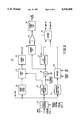
- the received RF signal is converted to an IF signal by a tuner 10, which is controlled by a microprocessor 12.
- Microprocessor 12 is responsive to user inputs, from either a keyboard 14 or an IR receiver 16, for applying appropriate signals to tuner 10 for tuning the selected channel.
- the IF signal including the pilot at 46.69 MHz, is applied from tuner 10 through a SAW filter 18, having a pass-band of about 41-47 MHz, to an IF amplifier and synchronous demodulator 20.
- the analog baseband output of demodulator 20 is coupled via a capacitor 21 to an analog to digital (A/D) converter 22, which samples the signal and provides the M-level symbols in binary form to a digital processor 24.
- A/D analog to digital
- Capacitor 21 eliminates the DC offset mentioned above from the A/D 22 input.
- A/D 22 is operated for sampling the output of demodulator 20 at the correct symbol times in response to a clock signal generated by digital processor 24.
- Digital processor 24 supplies the data and also supplies an AGC control signal to IF amplifier and synchronous demodulator 20 which, in turn, supplies a delayed AGC signal to tuner 10.
- Both demodulator 20 and digital processor 24 are responsive to an AFC Defeat signal generated by microprocessor 12 in response to selected start-up conditions, such as power-up, channel change and loss of data segment or frame synchronization.
- phase of the data output may be inverted because the FPLL in the synchronous demodulator is bi-phase stable, an automatic arrangement for providing the proper phase of data is also included. This is described more fully in connection with FIG. 5 and is claimed in copending application Ser. No. 08/174,867, above.
- IF amplifier and synchronous demodulator 20 is shown in more detail in FIG. 2.
- the IF signal from SAW filter 18 is applied through a gain controlled amplifier 30 to one input of an IF switch 32.
- the gain of amplifier 30 is controlled by an AGC control and charge pump 31.
- Circuit 31 is responsive to Gain-Up and Gain-Down signals for charging and discharging a capacitor 33 to a desired value for controlling the gain of amplifier 30.
- Circuit 31 also generates a delayed AGC signal for application to tuner 10.
- a crystal oscillator 34 is enabled in response to the AFC Defeat signal from microprocessor 12 for applying a relatively strong signal at the frequency of the pilot (46.69 MHz) to a second input of IF switch 32.
- IF switch 32 is also responsive to the AFC Defeat signal for coupling the output of crystal oscillator 34 to the switch output and is otherwise operable for coupling the output of IF amplifier 30 to its output.
- the output of IF switch 32 is the IF signal when the AFC Defeat signal is absent, and is the output of crystal oscillator 34 when the AFC Defeat signal is present.
- the output of IF switch 32 is applied to the first inputs of a pair of multipliers 40 and 42.
- a voltage controllable oscillator (VCO) 44 nominally generates an output at a frequency equal to 4 ⁇ pilot frequency (i.e. 186.76 MHz), which is applied to a divide-by-four prescaler circuit 46 for producing a pair of 90° phase-displaced signals at the pilot frequency.
- the in-phase (0°) signal is applied to the second input of multiplier 40 to produce an in-phase baseband component I and the quadrature (90°) signal is applied to the second input of multiplier 42 to produce a quadrature baseband component Q.
- the I and Q components are coupled through respective low-pass filters 50 and 52 to remove second harmonic mixer products, and amplified by respective amplifiers 54 and 56 to provide desired output levels.
- the amplified I and Q components are supplied to respective inputs of an FPLL 58, which is operated, in a well known manner, for generating a tuning voltage V t for locking the frequency and phase of the signal generated by VCO 44 to 4 times the pilot frequency.
- Capacitor 21 prevents the DC offset in the I channel signal from being applied to A/D 22. In this manner, the quadrature signals produced by divider 46 are locked to the pilot IF frequency for appropriately demodulating the received IF signal.
- the frequency of VCO 44 may be so far from its nominal frequency of 186.76 MHz that rapid lock-up by FPLL 58 in response to the relatively small received pilot cannot occur.
- FPLL 58 typically has a pull-in range of only about ⁇ 100 KHz at the IF frequency with the weak pilot signal, whereas its pull-in range with a strong signal is typically about ⁇ 750 KHz.
- the relatively strong 46.69 MHz output of crystal oscillator 34 is applied through IF switch 32 to the inputs of multipliers 40 and 42 during a start-up interval, which is defined by the AFC Defeat signal duration, rather than the received IF signal from IF amplifier 30.
- the start-up interval may be about 100 milliseconds (ms) long.
- a relatively strong signal at the frequency of the IF pilot is applied to the synchronous demodulator to allow FPLL 58 to rapidly bring the frequency of VCO 44 to its nominal value.
- the IF signal from amplifier 30 is applied to the synchronous demodulator by IF switch 32. Since VCO 44 is now very near the nominal demodulation frequency, FPLL 58 may readily lock VCO 44 to the frequency and phase of the received pilot to facilitate proper demodulation.
- the demodulated data is supplied from the I channel of synchronous demodulator 20, through capacitor 21, to the input of A/D 22 (FIG. 1).
- A/D 22 is responsive to a clock signal from digital processor 24 for sampling the analog I channel data signal at the correct sampling points and thereby providing a binary I channel data bit stream, representing the amplitudes of the received symbols, to the digital processor.
- the symbol values are preferably symmetrically disposed about a zero axis and the presence of any DC offset skews the values with respect to the zero axis. Therefore the A/D 22 needs to process amplitudes that are larger in one direction which requires a larger capacitor A/D.
- Elimination of the DC offset from the data channel by capacitor 21 permits the A/D 22 to see symmetrical inputs and consequently enables optimization of the size of A/D 22.
- the clock signal controlling sampling by A/D 22 is preferably generated as disclosed in copending application Ser. No. 07/894,388.
- the binary I channel data bit stream is applied to a polarity inverter 59 (controlled by a polarity invert control signal as will be described in FIG. 5) and thence to a symbol sync filter 60 and a sync correlation filter 62.
- Filter 60 is responsive to each segment sync character for producing a discriminator-type output having a zero-crossing at the center of the sync character.
- Filter 62 is configured for generating a relatively large pulse coinciding in time with the zero crossing of the output of filter 60.
- the output of filter 60 is gated into a PLL 64 by the pulse generated by filter 62.
- a symbol clock generator 66 is properly phased if the gated signal is zero.
- the receiver is operated in a noncoherent AGC mode for a short period after the start-up interval, and thereafter is operated in its normal, coherent AGC mode in another, much longer period corresponding to normal signal reception.
- These three periods are depicted in FIG. 4.
- the start-up interval i.e., the AFC Defeat signal is present
- the gain of amplifier 30 is rapidly reduced until a threshold level T is reached, after which the AGC is operated in its coherent mode in which the amplifier gain is controlled relatively slowly.
- a decoder 68 is responsive to the AFC Defeat signal for causing a second decoder 70 to generate a Gain-Up signal which is applied to charge pump 31 for rapidly increasing the gain of IF amplifier 30 independent of input signal strength.
- the binary I channel data signal which is being continually compared to a maximum value by a comparator 72 becomes effective. If the received data signal is equal to or exceeds the maximum value for eight consecutive symbols, decoder 68 generates an output causing decoder 70 to generate a Gain-Down signal for reducing the gain of amplifier 31 by a predetermined amount or step. This continues as long as the condition required by comparator 72 is satisfied.
- the receiver enters coherent AGC operation wherein the gain of amplifier 30 is controlled according to the strength of the received segment sync character, which is represented by the correlated pulse produced at the output of filter 62.
- the correlated pulse is applied to a polarity selection circuit in FIG. 5 to assure that the data polarity is correct since FPLL 58 can lock up in either of two phases.
- a reference level is subtracted from this correlated pulse in a summer 76 and the result is integrated in an AGC integrator 74, the output of which is applied to decoder 70 for controlling the gain of amplifier 31.
- a Gain-Down signal is generated by decoder 70 to reduce the gain of amplifier 31 and when the integrated signal falls below a second level a Gain-Up signal is generated by decoder 70 to increase the gain of amplifier 31.
- Integrator 74 is reset by decoder 70 after a Gain-Up or a Gain-Down signal is generated.
- the output of summer 76 is also applied to a segment sync integrator 94, the output of which is applied to one input of a comparator 96, the other input of which is supplied with a zero signal reference.
- the output of comparator 96 is supplied to a segment sync generator 98 for providing a segment sync output whenever the integrated correlation pulse from filter 62 is equal to or greater than a zero value.
- noncoherent AGC operation is relatively fast, being able to effect a gain change every eight symbol clocks.
- Coherent AGC operation is responsive to the segment sync character and can thus effect a gain change only once per data segment.
- non-coherent AGC operation has priority over coherent AGC operation. Thus, if the condition of comparator 72 is satisfied at any time (i.e. the I signal is equal to or greater than the maximum value for eight consecutive symbols), non-coherent mode AGC operation takes effect.
- the dual mode AGC operation is separately claimed in copending application Ser. No. 08/174,902, above.
- FPLL 58 in synchronous demodulator 20 is bi-phase stable. Consequently, the phase of the output data may be inverted.
- the polarity inverter 59 in digital processor 24 inverts the phase of the data signal, if necessary. Polarity inverter 59 is controlled by a signal from the polarity selection circuit shown in FIG. 5.
- the sign bit of the correlated sync pattern produced at the output of filter 62 is coupled to the D input of a first flip-flop 82, whose Q output is coupled to the D input of a second flip-flop 84 and to one input of a comparator 86, whose second input is supplied with the Q output of flip-flop 84.
- the output of comparator 86 is applied to the Reset input of a 3-bit counter 88, whose Carry output is coupled to one input of an AND gate 90.
- a second input of AND gate 90 is supplied with the Q output of flip-flop 82 and the output of the gate is coupled to the toggle input of a toggle flip-flop 92.
- the Q output of flip-flop 92 comprises the polarity invert control signal which controls the operation of polarity inverter 59.
- Flip-flops 82-84 and counter 88 are clocked by the segment sync signal derived from segment sync generator 98 (FIG. 3).
- the sign bit of the correlated output of filter 62 will be logic 0 when the output of synchronous demodulator 20 is properly phased. If the sign bit is logic 1, inverter 59 will be operated to invert the polarity of the data signal applied to digital processor 24.
- flip-flops 82 and 84 are operated for storing the sign bits of successive outputs of sync correlation filter 62.
- FIG. 6 shows a preferred embodiment of FPLL 58 (FIG. 2) which is also responsive to the AFC Defeat signal from microprocessor 12 as described hereinafter.
- the FPLL conventionally includes an AFC filter 80 comprising a series of resistors R1, R2 and R3 and capacitors C1, C2 and C3.
- the input of filter 80 is connected for receiving the demodulated I channel data signal and its output is connected to one input of a limiter 82, the other input of limiter 82 being supplied with a reference voltage.
- the output of limiter 82 is supplied to one input of a multiplier 84.
- the demodulated Q signal is supplied to a second input of multiplier 84, whose output is connected to a PLL filter 86, which generates the voltage V t for controlling VCO 44 (FIG. 2).
- AFC filter 80 has amplitude and phase versus frequency response characteristics as shown in solid line in FIGS. 7A and 7B, respectively, for (1) rejecting the high frequency data components in the I channel data signal and (2) providing a phase shift of the input signal.
- An error in the frequency of VCO 44 from its nominal demodulating frequency is reflected in the production of beat frequencies in the I and Q signals.
- AFC filter 80 will produce an output of sufficient amplitude and phase to allow for correction of the VCO frequency.
- Such correction is effected by multiplying the limited output of AFC filter 80 with the Q signal to supply a frequency correction signal to PLL filter 86.
- AFC filter 80 provides an increased level output signal having a phase shift of less than 180° (i.e., about 90°) to facilitate carrier acquisition in response to the output of crystal oscillator 34 during the start-up interval.
Abstract
Description
Claims (32)
Priority Applications (9)
| Application Number | Priority Date | Filing Date | Title |
|---|---|---|---|
| US08/175,333 US5410368A (en) | 1993-12-29 | 1993-12-29 | Carrier acquisition by applying substitute pilot to a synchronous demodulator during a start up interval |
| PCT/US1994/014393 WO1995018508A1 (en) | 1993-12-29 | 1994-12-15 | Circuit for the acquisition of a carrier signal by applying a substitute pilot to a synchronous demodulator |
| CA002296855A CA2296855C (en) | 1993-12-29 | 1994-12-15 | Receiving and demodulating a digital television signal |
| CN94194684A CN1109439C (en) | 1993-12-29 | 1994-12-15 | Circuit for the acquisition of a carrier signal by applying a substitute pilot to a synchronous demodulator |
| CA002296861A CA2296861C (en) | 1993-12-29 | 1994-12-15 | Television receiver for tuning a signal including a pilot signal |
| JP51807095A JP3399533B2 (en) | 1993-12-29 | 1994-12-15 | Television receiver for tuning television signals, including pilot signals |
| CA002178198A CA2178198C (en) | 1993-12-29 | 1994-12-15 | Circuit for the acquisition of a carrier signal by applying a substitute pilot to a synchronous demodulator |
| KR1019960703484A KR100274290B1 (en) | 1993-12-29 | 1994-12-15 | A television receiver for tuning a television signal |
| US08/345,886 US5638140A (en) | 1993-12-29 | 1995-01-27 | FPLL having AFC filter with limited phase shift |
Applications Claiming Priority (1)
| Application Number | Priority Date | Filing Date | Title |
|---|---|---|---|
| US08/175,333 US5410368A (en) | 1993-12-29 | 1993-12-29 | Carrier acquisition by applying substitute pilot to a synchronous demodulator during a start up interval |
Related Child Applications (1)
| Application Number | Title | Priority Date | Filing Date |
|---|---|---|---|
| US08/345,886 Division US5638140A (en) | 1993-12-29 | 1995-01-27 | FPLL having AFC filter with limited phase shift |
Publications (1)
| Publication Number | Publication Date |
|---|---|
| US5410368A true US5410368A (en) | 1995-04-25 |
Family
ID=22639879
Family Applications (2)
| Application Number | Title | Priority Date | Filing Date |
|---|---|---|---|
| US08/175,333 Expired - Lifetime US5410368A (en) | 1993-12-29 | 1993-12-29 | Carrier acquisition by applying substitute pilot to a synchronous demodulator during a start up interval |
| US08/345,886 Expired - Lifetime US5638140A (en) | 1993-12-29 | 1995-01-27 | FPLL having AFC filter with limited phase shift |
Family Applications After (1)
| Application Number | Title | Priority Date | Filing Date |
|---|---|---|---|
| US08/345,886 Expired - Lifetime US5638140A (en) | 1993-12-29 | 1995-01-27 | FPLL having AFC filter with limited phase shift |
Country Status (6)
| Country | Link |
|---|---|
| US (2) | US5410368A (en) |
| JP (1) | JP3399533B2 (en) |
| KR (1) | KR100274290B1 (en) |
| CN (1) | CN1109439C (en) |
| CA (3) | CA2178198C (en) |
| WO (1) | WO1995018508A1 (en) |
Cited By (26)
| Publication number | Priority date | Publication date | Assignee | Title |
|---|---|---|---|---|
| WO1995026101A1 (en) * | 1994-03-21 | 1995-09-28 | Rca Thomson Licensing Corporation | Carrier recovery system for a vestigial sideband signal |
| US5508748A (en) * | 1993-02-08 | 1996-04-16 | Zenith Electronics Corporation | Data level selection for multilevel VSB transmission system |
| US5565932A (en) * | 1994-11-08 | 1996-10-15 | Zenith Electronics Corp. | AGC system with pilot using digital data reference |
| US5570137A (en) * | 1994-05-20 | 1996-10-29 | Ant Nachrichtentechnik Gmbh | Device for digital demodulation of video and audio elements of television signal |
| US5648923A (en) * | 1995-03-02 | 1997-07-15 | Hitachi America, Ltd. | Nyquist filter for use in a joint VSB/QAM demodulator |
| US5673293A (en) * | 1994-09-08 | 1997-09-30 | Hitachi America, Ltd. | Method and apparatus for demodulating QAM and VSB signals |
| US5699011A (en) * | 1996-08-02 | 1997-12-16 | Zenith Electronics Corporation | DC offset compensation method and apparatus |
| US5745528A (en) * | 1995-07-13 | 1998-04-28 | Zenith Electronics Corporation | VSB mode selection system |
| US5894334A (en) * | 1994-03-21 | 1999-04-13 | Rca Thomson Licensing Corporation | Carrier recovery system for a vestigial sideband signal |
| WO1999023821A1 (en) * | 1997-10-31 | 1999-05-14 | Thomson Licensing S.A. | Network for eliminating dc offset in a received hdtv signal |
| FR2798017A1 (en) * | 1999-08-30 | 2001-03-02 | Sharp Kk | Satellite receiver digital broadcast receiver phase shifter having two signal paths phase shift separated and frequency multiplier producing two local oscillator signals 90 degrees phase shift separated. |
| US6219088B1 (en) | 1998-11-03 | 2001-04-17 | Broadcom Corporation | NTSC interference rejection filter |
| US6222891B1 (en) | 1998-11-03 | 2001-04-24 | Broadcom Corporation | Timing recovery using the pilot signal in high definition TV |
| US6226323B1 (en) | 1998-11-03 | 2001-05-01 | Broadcom Corporation | Technique for minimizing decision feedback equalizer wordlength in the presence of a DC component |
| USRE37326E1 (en) * | 1994-04-12 | 2001-08-14 | Lg Electronics | HDTV receiver |
| US6313885B1 (en) * | 1998-03-25 | 2001-11-06 | Samsung Electronics Co., Ltd. | DTV receiver with baseband equalization filters for QAM signal and for VSB signal which employ common elements |
| US6421098B1 (en) * | 1999-03-12 | 2002-07-16 | Sony Corporation | Method and apparatus for changing automatic gain control points of digital television signals |
| US6496229B1 (en) * | 1998-04-02 | 2002-12-17 | Samsung Electronics Co., Ltd. | TV receiver using read-only memory shared during VSB and QAM reception for synchrodyning I-F signal to baseband |
| US6512555B1 (en) * | 1994-05-04 | 2003-01-28 | Samsung Electronics Co., Ltd. | Radio receiver for vestigal-sideband amplitude-modulation digital television signals |
| US6545728B1 (en) * | 1994-05-04 | 2003-04-08 | Samsung Electronics Co., Ltd. | Digital television receivers that digitize final I-F signals resulting from triple-conversion |
| US20040022331A1 (en) * | 2002-07-31 | 2004-02-05 | Taarud Jeff E. | Method for mitigating DC offset in a sign bit correlator |
| US6775334B1 (en) | 1998-11-03 | 2004-08-10 | Broadcom Corporation | Equalization and decision-directed loops with trellis demodulation in high definition TV |
| US20040196897A1 (en) * | 1998-11-03 | 2004-10-07 | Broadcom Corporation | Technique for minimizing decision feedback equalizer wordlength in the presence of a DC component |
| US6842495B1 (en) | 1998-11-03 | 2005-01-11 | Broadcom Corporation | Dual mode QAM/VSB receiver |
| US6879627B1 (en) * | 2000-06-01 | 2005-04-12 | Shiron Satellite Communications (1996) Ltd. | Variable rate continuous mode satellite modem |
| US20070146553A1 (en) * | 2005-12-28 | 2007-06-28 | Matsushita Electric Industrial Co., Ltd. | Receiving circuit, receiving apparatus, and receiving method |
Families Citing this family (18)
| Publication number | Priority date | Publication date | Assignee | Title |
|---|---|---|---|---|
| KR0157531B1 (en) * | 1995-07-14 | 1998-11-16 | 김광호 | Digital carrier wave restoring apparatus and method at tv signal receiver |
| JP3225837B2 (en) * | 1996-04-19 | 2001-11-05 | 松下電器産業株式会社 | High frequency signal receiver |
| JPH10248040A (en) * | 1997-03-05 | 1998-09-14 | Sanyo Electric Co Ltd | Television receiver |
| US6061096A (en) * | 1997-03-19 | 2000-05-09 | Samsung Electronics Co., Ltd. | Digital-and-analog-TV-signal receivers, each with single first detector and shared high-band I-F amplification |
| US6055280A (en) * | 1997-06-27 | 2000-04-25 | Raytheon Company | High data rate digital demodulator and bit synchronizer |
| US6751272B1 (en) * | 1998-02-11 | 2004-06-15 | 3Com Corporation | Dynamic adjustment to preserve signal-to-noise ratio in a quadrature detector system |
| KR100252987B1 (en) * | 1998-03-12 | 2000-04-15 | 구자홍 | Digital tv receiver |
| JP2000115263A (en) * | 1998-09-30 | 2000-04-21 | Matsushita Electric Ind Co Ltd | Digital broadcast demodulator |
| JP2001077671A (en) * | 1999-07-06 | 2001-03-23 | Matsushita Electric Ind Co Ltd | Device and method for digital broadcast channel selection |
| EP1197077B8 (en) * | 1999-07-16 | 2005-11-30 | Thomson Licensing | Selective gain adjustement to aid carrier acquisition in a high definition television receiver |
| KR100364783B1 (en) * | 2000-07-28 | 2002-12-16 | 엘지전자 주식회사 | digital television receiver and method for controlling to antenna in digital television receiver |
| US7079591B2 (en) | 2001-08-01 | 2006-07-18 | Radiodetection Limited | Method and system for recovering information from a magnetic field signal usable for locating an underground object |
| JP3586267B2 (en) * | 2002-06-18 | 2004-11-10 | 沖電気工業株式会社 | Automatic gain control circuit |
| JP4979025B2 (en) * | 2005-11-04 | 2012-07-18 | トムソン ライセンシング | Apparatus and method for detecting low signal-to-noise ratio ATSC signals |
| US20090232759A1 (en) * | 2005-12-16 | 2009-09-17 | Fraser Ian Bell | Hair Treatment Compositions |
| US7937053B2 (en) * | 2007-06-08 | 2011-05-03 | Himax Technologies Limited | Method for receiving station signal and receiver for receiving the same |
| CN109004930A (en) * | 2018-09-29 | 2018-12-14 | 清华大学 | Circuit system and control method based on the direct frequency, demodulation frequency modulated signal of phaselocked loop |
| CN112542996A (en) * | 2019-09-20 | 2021-03-23 | 中国科学院微电子研究所 | High-order synchronous integral demodulation circuit and method for gyro digital signal |
Citations (4)
| Publication number | Priority date | Publication date | Assignee | Title |
|---|---|---|---|---|
| US3644853A (en) * | 1970-11-23 | 1972-02-22 | Zenith Radio Corp | Voltage-controlled signal-seeking tuning system |
| US4443769A (en) * | 1981-04-27 | 1984-04-17 | Rca Corporation | Frequency search system for a phase locked loop |
| US4939790A (en) * | 1988-03-28 | 1990-07-03 | Zenith Electronics Corporation | PLL frequency stabilization in data packet receivers |
| US5105273A (en) * | 1989-07-12 | 1992-04-14 | Mitsubishi Denki Kabushiki Kaisha | Video intermediate frequency signal processing circuit |
Family Cites Families (10)
| Publication number | Priority date | Publication date | Assignee | Title |
|---|---|---|---|---|
| CH566089A5 (en) * | 1973-12-20 | 1975-08-29 | Hasler Ag | |
| US4823399A (en) * | 1987-07-30 | 1989-04-18 | General Instrument Corporation | Refined tuning of RF receiver with frequency-locked loop |
| US4849993A (en) * | 1987-12-10 | 1989-07-18 | Silicon General, Inc. | Clock holdover circuit |
| US4918718A (en) * | 1988-06-28 | 1990-04-17 | Luma Telecom, Inc. | Quadrature amplitude modulation with line synchronization pulse for video telephone |
| US4945415A (en) * | 1988-08-29 | 1990-07-31 | Motorola, Inc. | Slew enhancement circuit for an automatic frequency control system |
| US5087975A (en) * | 1990-11-09 | 1992-02-11 | Zenith Electronics Corporation | VSB HDTV transmission system with reduced NTSC co-channel interference |
| JPH04239804A (en) * | 1991-01-24 | 1992-08-27 | Matsushita Electric Ind Co Ltd | Demodulation circuit |
| US5287180A (en) * | 1991-02-04 | 1994-02-15 | General Electric Company | Modulator/demodulater for compatible high definition television system |
| US5181112A (en) * | 1991-03-11 | 1993-01-19 | Zenith Electronics Corporation | Television signal transmission system with carrier offset compensation |
| US5175626A (en) * | 1991-07-25 | 1992-12-29 | Rca Thomson Licensing Corporation | Apparatus providing a clock signal for a digital television receiver in response to a channel change |
-
1993
- 1993-12-29 US US08/175,333 patent/US5410368A/en not_active Expired - Lifetime
-
1994
- 1994-12-15 WO PCT/US1994/014393 patent/WO1995018508A1/en active Application Filing
- 1994-12-15 CN CN94194684A patent/CN1109439C/en not_active Expired - Lifetime
- 1994-12-15 JP JP51807095A patent/JP3399533B2/en not_active Expired - Lifetime
- 1994-12-15 KR KR1019960703484A patent/KR100274290B1/en not_active IP Right Cessation
- 1994-12-15 CA CA002178198A patent/CA2178198C/en not_active Expired - Lifetime
- 1994-12-15 CA CA002296861A patent/CA2296861C/en not_active Expired - Lifetime
- 1994-12-15 CA CA002296855A patent/CA2296855C/en not_active Expired - Lifetime
-
1995
- 1995-01-27 US US08/345,886 patent/US5638140A/en not_active Expired - Lifetime
Patent Citations (4)
| Publication number | Priority date | Publication date | Assignee | Title |
|---|---|---|---|---|
| US3644853A (en) * | 1970-11-23 | 1972-02-22 | Zenith Radio Corp | Voltage-controlled signal-seeking tuning system |
| US4443769A (en) * | 1981-04-27 | 1984-04-17 | Rca Corporation | Frequency search system for a phase locked loop |
| US4939790A (en) * | 1988-03-28 | 1990-07-03 | Zenith Electronics Corporation | PLL frequency stabilization in data packet receivers |
| US5105273A (en) * | 1989-07-12 | 1992-04-14 | Mitsubishi Denki Kabushiki Kaisha | Video intermediate frequency signal processing circuit |
Cited By (45)
| Publication number | Priority date | Publication date | Assignee | Title |
|---|---|---|---|---|
| US5508748A (en) * | 1993-02-08 | 1996-04-16 | Zenith Electronics Corporation | Data level selection for multilevel VSB transmission system |
| WO1995026101A1 (en) * | 1994-03-21 | 1995-09-28 | Rca Thomson Licensing Corporation | Carrier recovery system for a vestigial sideband signal |
| US5894334A (en) * | 1994-03-21 | 1999-04-13 | Rca Thomson Licensing Corporation | Carrier recovery system for a vestigial sideband signal |
| USRE37326E1 (en) * | 1994-04-12 | 2001-08-14 | Lg Electronics | HDTV receiver |
| US6512555B1 (en) * | 1994-05-04 | 2003-01-28 | Samsung Electronics Co., Ltd. | Radio receiver for vestigal-sideband amplitude-modulation digital television signals |
| US6545728B1 (en) * | 1994-05-04 | 2003-04-08 | Samsung Electronics Co., Ltd. | Digital television receivers that digitize final I-F signals resulting from triple-conversion |
| US5570137A (en) * | 1994-05-20 | 1996-10-29 | Ant Nachrichtentechnik Gmbh | Device for digital demodulation of video and audio elements of television signal |
| US5673293A (en) * | 1994-09-08 | 1997-09-30 | Hitachi America, Ltd. | Method and apparatus for demodulating QAM and VSB signals |
| AU691695B2 (en) * | 1994-11-08 | 1998-05-21 | Zenith Electronics Corporation | Agc circuit for a digital receiver |
| US5565932A (en) * | 1994-11-08 | 1996-10-15 | Zenith Electronics Corp. | AGC system with pilot using digital data reference |
| US5648923A (en) * | 1995-03-02 | 1997-07-15 | Hitachi America, Ltd. | Nyquist filter for use in a joint VSB/QAM demodulator |
| US5745528A (en) * | 1995-07-13 | 1998-04-28 | Zenith Electronics Corporation | VSB mode selection system |
| US5987070A (en) * | 1995-07-13 | 1999-11-16 | Zenith Electronics Corporation | VSB mode selection system |
| US5699011A (en) * | 1996-08-02 | 1997-12-16 | Zenith Electronics Corporation | DC offset compensation method and apparatus |
| WO1999023821A1 (en) * | 1997-10-31 | 1999-05-14 | Thomson Licensing S.A. | Network for eliminating dc offset in a received hdtv signal |
| US6313885B1 (en) * | 1998-03-25 | 2001-11-06 | Samsung Electronics Co., Ltd. | DTV receiver with baseband equalization filters for QAM signal and for VSB signal which employ common elements |
| US6496229B1 (en) * | 1998-04-02 | 2002-12-17 | Samsung Electronics Co., Ltd. | TV receiver using read-only memory shared during VSB and QAM reception for synchrodyning I-F signal to baseband |
| US20040081257A1 (en) * | 1998-11-03 | 2004-04-29 | Broadcom Corporation | Phase detectors in carrier recovery for offset QAM and VSB |
| US6842495B1 (en) | 1998-11-03 | 2005-01-11 | Broadcom Corporation | Dual mode QAM/VSB receiver |
| US6771714B2 (en) | 1998-11-03 | 2004-08-03 | Broadcom Corporation | Timing recovery using the pilot signal in high definition TV |
| US8098725B2 (en) | 1998-11-03 | 2012-01-17 | Broadcom Corporation | Equalization and decision-directed loops with trellis demodulation in high definition TV |
| US6493409B1 (en) | 1998-11-03 | 2002-12-10 | Broadcom Corporation | Phase detectors in carrier recovery for offset QAM and VSB |
| US6222891B1 (en) | 1998-11-03 | 2001-04-24 | Broadcom Corporation | Timing recovery using the pilot signal in high definition TV |
| US6219088B1 (en) | 1998-11-03 | 2001-04-17 | Broadcom Corporation | NTSC interference rejection filter |
| US6226323B1 (en) | 1998-11-03 | 2001-05-01 | Broadcom Corporation | Technique for minimizing decision feedback equalizer wordlength in the presence of a DC component |
| US6775334B1 (en) | 1998-11-03 | 2004-08-10 | Broadcom Corporation | Equalization and decision-directed loops with trellis demodulation in high definition TV |
| US20090086808A1 (en) * | 1998-11-03 | 2009-04-02 | Broadcom Corporation | Equalization And Decision-Directed Loops With Trellis Demodulation In High Definition TV |
| US7327819B2 (en) | 1998-11-03 | 2008-02-05 | Broadcom Corporation | Phase detectors in carrier recovery for offset QAM and VSB |
| US7277481B2 (en) | 1998-11-03 | 2007-10-02 | Broadcom Corporation | Technique for minimizing decision feedback equalizer wordlength in the presence of a DC component |
| US6671342B2 (en) | 1998-11-03 | 2003-12-30 | Broadcom Corporation | Phase detectors in carrier recovery for offset QAM and VSB |
| US20040196897A1 (en) * | 1998-11-03 | 2004-10-07 | Broadcom Corporation | Technique for minimizing decision feedback equalizer wordlength in the presence of a DC component |
| US20040258184A1 (en) * | 1998-11-03 | 2004-12-23 | Broadcom Corporation | Equalization and decision-directed loops with trellis demodulation in high definition TV |
| US20040258180A1 (en) * | 1998-11-03 | 2004-12-23 | Broadcom Corporation | Timing recovery using the pilot signal in high definition TV |
| US6411659B1 (en) | 1998-11-03 | 2002-06-25 | Broadcom Corporation | Timing recovery using the pilot signal in high definition TV |
| US7474695B2 (en) | 1998-11-03 | 2009-01-06 | Broadcom Corporation | Equalization and decision-directed loops with trellis demodulation in high definition TV |
| US20050105651A1 (en) * | 1998-11-03 | 2005-05-19 | Jaffe Steven T. | Dual mode QAM/VSB receiver |
| US7403579B2 (en) | 1998-11-03 | 2008-07-22 | Broadcom Corporation | Dual mode QAM/VSB receiver |
| US7027528B2 (en) | 1998-11-03 | 2006-04-11 | Broadcom Corporation | Timing recovery using the pilot signal in high definition TV |
| US6421098B1 (en) * | 1999-03-12 | 2002-07-16 | Sony Corporation | Method and apparatus for changing automatic gain control points of digital television signals |
| FR2798017A1 (en) * | 1999-08-30 | 2001-03-02 | Sharp Kk | Satellite receiver digital broadcast receiver phase shifter having two signal paths phase shift separated and frequency multiplier producing two local oscillator signals 90 degrees phase shift separated. |
| US6433630B1 (en) * | 1999-08-30 | 2002-08-13 | Sharp Kabushiki Kaisha | Phase shifter, and demodulator employing it |
| US6879627B1 (en) * | 2000-06-01 | 2005-04-12 | Shiron Satellite Communications (1996) Ltd. | Variable rate continuous mode satellite modem |
| US6999534B2 (en) * | 2002-07-31 | 2006-02-14 | Texas Instruments Incorporated | Method for mitigating DC offset in a sign bit correlator |
| US20040022331A1 (en) * | 2002-07-31 | 2004-02-05 | Taarud Jeff E. | Method for mitigating DC offset in a sign bit correlator |
| US20070146553A1 (en) * | 2005-12-28 | 2007-06-28 | Matsushita Electric Industrial Co., Ltd. | Receiving circuit, receiving apparatus, and receiving method |
Also Published As
| Publication number | Publication date |
|---|---|
| CN1109439C (en) | 2003-05-21 |
| JPH09509020A (en) | 1997-09-09 |
| JP3399533B2 (en) | 2003-04-21 |
| WO1995018508A1 (en) | 1995-07-06 |
| US5638140A (en) | 1997-06-10 |
| CA2296855A1 (en) | 1995-07-06 |
| CA2178198C (en) | 2000-05-02 |
| CA2296861A1 (en) | 1995-07-06 |
| CN1139507A (en) | 1997-01-01 |
| CA2296855C (en) | 2001-02-20 |
| CA2296861C (en) | 2001-02-20 |
| KR100274290B1 (en) | 2000-12-15 |
Similar Documents
| Publication | Publication Date | Title |
|---|---|---|
| US5410368A (en) | Carrier acquisition by applying substitute pilot to a synchronous demodulator during a start up interval | |
| US5584068A (en) | Direct conversion receiver | |
| JP2971033B2 (en) | Apparatus and method for restoring digital carrier in television signal receiver | |
| US5402449A (en) | Process and device for converting digitally modulate high-frequency reception signals | |
| US4816769A (en) | BPSK demodulator and FM receiver for digital data pagers | |
| US6069524A (en) | FPLL with third multiplier in an analog input signal | |
| US6731698B1 (en) | Quadrature demodulation circuit capable for canceling offset | |
| US5546138A (en) | AGC system with overriding, maximum gain during an initial interval to enhance signal acquisition | |
| US5627604A (en) | Stabilizing the lock up of a bi-phase stable FPLL by augmenting a recovered DC pilot | |
| US5621483A (en) | Polarity selection circuit for bi-phase stable FPLL | |
| CA2134531A1 (en) | Control arrangements for digital radio receivers | |
| US4517531A (en) | Carrier wave reproducing circuit in synchronized detection system of medium speed facsimile | |
| IE894026L (en) | Digital automatic frequency control on pure sine waves | |
| US5644606A (en) | Receiver with two synchronization loops | |
| US5809096A (en) | Digital transmission system comprising decision means for changing the synchronization mode | |
| US5745004A (en) | FPLL with third multiplier in an AC path in the FPLL | |
| MXPA96004558A (en) | Receiver and method for stabilizing a demodulator by increasing a cd recobr pilot component | |
| US6593974B1 (en) | Circuit arrangement for demodulating an intermediate-frequency video signal | |
| JP2687851B2 (en) | Receiving machine | |
| KR0153604B1 (en) | Frequency and phase automatic regulation circuit and method of receiver | |
| US5881111A (en) | Frequency sweep circuit | |
| US5668498A (en) | Controlling FPLL polarity using pilot signal and polarity inverter | |
| KR0159440B1 (en) | A circuit and method for restorating frequency offset of receiver | |
| KR19980018519A (en) | Circuitry for locking frequency and phase locking circuitry to a desired phase | |
| JP2865760B2 (en) | Satellite receiver |
Legal Events
| Date | Code | Title | Description |
|---|---|---|---|
| AS | Assignment |
Owner name: ZENITH ELECTRONICS CORP., ILLINOIS Free format text: ASSIGNMENT OF ASSIGNORS INTEREST;ASSIGNORS:KRISHNAMURTHY, GOPALAN;MYCYNEK, VICTOR G.;SGRIGNOLI, GARY J.;REEL/FRAME:006856/0512 Effective date: 19931228 |
|
| STCF | Information on status: patent grant |
Free format text: PATENTED CASE |
|
| AS | Assignment |
Owner name: CITICORP NORTH AMERICA, INC., AS AGENT, NEW YORK Free format text: PATENT COLLATERAL ASSIGNMENT AND SECURITY AGREEMENT.;ASSIGNOR:ZENITH ELECTRONICS CORPORATION;REEL/FRAME:010033/0321 Effective date: 19980331 |
|
| AS | Assignment |
Owner name: LG ELECTRONICS INC., KOREA, REPUBLIC OF Free format text: PATENT COLLATERAL ASSIGNMENT AND SECURITY AGREEMENT. RE-RECORD TO CORRECT THE RECORDATION DATE OF 07/28/98 TO 05/05/98 PREVIOUSLY RECORDED AT REEL 9367, FRAME 0067.;ASSIGNOR:ZENITH ELECTRONICS CORPORATION;REEL/FRAME:009423/0216 Effective date: 19980429 |
|
| AS | Assignment |
Owner name: LG ELECTRONICS INC., KOREA, REPUBLIC OF Free format text: ;ASSIGNOR:ZENITH ELECTRONICS CORPORATIOIN;REEL/FRAME:009367/0060 Effective date: 19980429 |
|
| FPAY | Fee payment |
Year of fee payment: 4 |
|
| AS | Assignment |
Owner name: CITICORP NORTH AMERICA, INC., AS AGENT, NEW YORK Free format text: SECURITY AGREEMENT;ASSIGNOR:ZENITH ELECTRONICS CORPORATION;REEL/FRAME:010470/0414 Effective date: 19991109 |
|
| AS | Assignment |
Owner name: LG ELECTRONICS INC., KOREA, REPUBLIC OF Free format text: SECURITY AGREEMENT;ASSIGNOR:ZENITH ELECTRONICS CORPORATION;REEL/FRAME:010618/0424 Effective date: 19991109 |
|
| AS | Assignment |
Owner name: ZENITH ELECTRONICS CORPORATION, ILLINOIS Free format text: RELEASE OF SECURITY INTEREST;ASSIGNOR:CITICORP NORTH AMERICA, INC.;REEL/FRAME:012188/0204 Effective date: 20010822 |
|
| FPAY | Fee payment |
Year of fee payment: 8 |
|
| FEPP | Fee payment procedure |
Free format text: PAYOR NUMBER ASSIGNED (ORIGINAL EVENT CODE: ASPN); ENTITY STATUS OF PATENT OWNER: LARGE ENTITY |
|
| FPAY | Fee payment |
Year of fee payment: 12 |