US5469434A - Distributed frame processing for time division multiplexing - Google Patents
Distributed frame processing for time division multiplexing Download PDFInfo
- Publication number
- US5469434A US5469434A US08/007,074 US707493A US5469434A US 5469434 A US5469434 A US 5469434A US 707493 A US707493 A US 707493A US 5469434 A US5469434 A US 5469434A
- Authority
- US
- United States
- Prior art keywords
- data
- bus
- time division
- frame
- pri
- Prior art date
- Legal status (The legal status is an assumption and is not a legal conclusion. Google has not performed a legal analysis and makes no representation as to the accuracy of the status listed.)
- Expired - Fee Related
Links
- 238000012545 processing Methods 0.000 title claims description 8
- 238000004891 communication Methods 0.000 claims abstract description 78
- 238000009432 framing Methods 0.000 claims abstract description 13
- 230000001360 synchronised effect Effects 0.000 claims abstract description 3
- 230000002457 bidirectional effect Effects 0.000 claims description 4
- 238000012544 monitoring process Methods 0.000 claims 1
- 230000007246 mechanism Effects 0.000 description 56
- 230000006870 function Effects 0.000 description 15
- 238000012546 transfer Methods 0.000 description 14
- 238000012360 testing method Methods 0.000 description 10
- 101100521097 Caenorhabditis elegans pri-1 gene Proteins 0.000 description 5
- 101100353170 Caenorhabditis elegans pri-2 gene Proteins 0.000 description 5
- 238000003860 storage Methods 0.000 description 5
- 238000010586 diagram Methods 0.000 description 4
- 238000000034 method Methods 0.000 description 4
- 230000008569 process Effects 0.000 description 4
- 239000002131 composite material Substances 0.000 description 3
- 101100172879 Caenorhabditis elegans sec-5 gene Proteins 0.000 description 2
- 101100172886 Caenorhabditis elegans sec-6 gene Proteins 0.000 description 2
- 101100172892 Caenorhabditis elegans sec-8 gene Proteins 0.000 description 2
- 230000005540 biological transmission Effects 0.000 description 2
- 239000000872 buffer Substances 0.000 description 2
- 230000004048 modification Effects 0.000 description 2
- 238000012986 modification Methods 0.000 description 2
- GRNHLFULJDXJKR-UHFFFAOYSA-N 3-(2-sulfanylethyl)-1h-quinazoline-2,4-dione Chemical compound C1=CC=C2C(=O)N(CCS)C(=O)NC2=C1 GRNHLFULJDXJKR-UHFFFAOYSA-N 0.000 description 1
- 101001022148 Homo sapiens Furin Proteins 0.000 description 1
- 101000701936 Homo sapiens Signal peptidase complex subunit 1 Proteins 0.000 description 1
- 101100353177 Schizosaccharomyces pombe (strain 972 / ATCC 24843) spp2 gene Proteins 0.000 description 1
- 102100030313 Signal peptidase complex subunit 1 Human genes 0.000 description 1
- 101150056647 TNFRSF4 gene Proteins 0.000 description 1
- 238000004364 calculation method Methods 0.000 description 1
- 230000008859 change Effects 0.000 description 1
- 239000004020 conductor Substances 0.000 description 1
- 238000013500 data storage Methods 0.000 description 1
- 238000003745 diagnosis Methods 0.000 description 1
- 238000009826 distribution Methods 0.000 description 1
- 230000009977 dual effect Effects 0.000 description 1
- 238000004519 manufacturing process Methods 0.000 description 1
- 101150047682 priL gene Proteins 0.000 description 1
- 101150103950 priS gene Proteins 0.000 description 1
- 230000000630 rising effect Effects 0.000 description 1
- 230000011664 signaling Effects 0.000 description 1
Images


Classifications
-
- H—ELECTRICITY
- H04—ELECTRIC COMMUNICATION TECHNIQUE
- H04L—TRANSMISSION OF DIGITAL INFORMATION, e.g. TELEGRAPHIC COMMUNICATION
- H04L12/00—Data switching networks
- H04L12/50—Circuit switching systems, i.e. systems in which the path is physically permanent during the communication
- H04L12/52—Circuit switching systems, i.e. systems in which the path is physically permanent during the communication using time division techniques
-
- H—ELECTRICITY
- H04—ELECTRIC COMMUNICATION TECHNIQUE
- H04J—MULTIPLEX COMMUNICATION
- H04J3/00—Time-division multiplex systems
- H04J3/02—Details
- H04J3/06—Synchronising arrangements
- H04J3/0635—Clock or time synchronisation in a network
- H04J3/0685—Clock or time synchronisation in a node; Intranode synchronisation
-
- H—ELECTRICITY
- H04—ELECTRIC COMMUNICATION TECHNIQUE
- H04J—MULTIPLEX COMMUNICATION
- H04J3/00—Time-division multiplex systems
- H04J3/16—Time-division multiplex systems in which the time allocation to individual channels within a transmission cycle is variable, e.g. to accommodate varying complexity of signals, to vary number of channels transmitted
- H04J3/1605—Fixed allocated frame structures
- H04J3/1623—Plesiochronous digital hierarchy [PDH]
- H04J3/1641—Hierarchical systems
-
- Y—GENERAL TAGGING OF NEW TECHNOLOGICAL DEVELOPMENTS; GENERAL TAGGING OF CROSS-SECTIONAL TECHNOLOGIES SPANNING OVER SEVERAL SECTIONS OF THE IPC; TECHNICAL SUBJECTS COVERED BY FORMER USPC CROSS-REFERENCE ART COLLECTIONS [XRACs] AND DIGESTS
- Y10—TECHNICAL SUBJECTS COVERED BY FORMER USPC
- Y10S—TECHNICAL SUBJECTS COVERED BY FORMER USPC CROSS-REFERENCE ART COLLECTIONS [XRACs] AND DIGESTS
- Y10S370/00—Multiplex communications
- Y10S370/914—Rate converter
Definitions
- This invention relates generally to telecommunications systems. More particularly, the present invention relates to time-division-multiplexers (TDMs).
- TDMs time-division-multiplexers
- TDM systems are used for multiplexing information present on a plurality of input channels onto a single output or aggregate data channel.
- This multiplexing function is generally achieved by the use of a data "frame" to efficiently allocate and combine the incoming data from the input channels into the aggregate channel.
- An example of a framing algorithm for allocating the data from a plurality of input channels to an aggregate channel is disclosed in U.S. Pat. No. 4,881,224 to Bains, which is hereby incorporated herein by reference in its entirety.
- a central processor and a plurality of channel modules are provided.
- the incoming channels are coupled to the individual channel modules.
- Each channel module is typically coupled to the central processor via a data bus and an address bus.
- the central processor generates and contains the framing algorithm.
- the central processor executes the framing algorithm by communicating with the channel modules.
- the central processor uses the address bus to inform the channel modules as to the particular times they are to place information on a data bus.
- the central processor places an address on the address bus, and the channel module at that address is then permitted to place information on the data bus.
- bit interleaved multiplexers the information placed by the channel module onto the data bus is a single bit of information at a time. It will be appreciated that in byte interleaved multiplexers, when the address of the channel module is indicated, a whole byte of information may be placed onto the data bus.
- the central processor With the prior art systems, large burdens are placed on the central processor. Not only does the central processor have to supervise the time division multiplexing of data onto the data bus by quickly generating and sending source and destination addresses to the channel modules via the address bus according to the determined framing algorithm, but the central processor typically is utilized to check the status of the various channel modules and to test that they are functioning properly. While at relatively slow speeds these functions may be readily accomplished, at high TDM rates, difficulties arise.
- Another object of the invention is to provide a time division multiplexing system where the framing algorithm for the system is communicated by a central processor to each of the channel modules over the time division multiplexed data bus which carries data.
- the TDM system for multiplexing data from a plurality of channels.
- the TDM system generally comprises a high speed time division multiplexed digital data bus, a plurality of channel cards coupled between the data channels and the data bus with each channel card having its own processor and memory, and a system communication manager which is also coupled to the digital bus, and includes a microprocessor.
- the processor of the common control module determines the frame for the system and initially forwards the frame information to each of the channel cards during predetermined time slots of the high speed time division multiplexed digital data bus.
- the channel cards are synchronized by the communication manager via a synchronization bus, and the channel cards use the synchronization information and the framing information in order to appropriately place data on and take data off of the high speed data bus without ever being addressed by an address bus. More particularly, where the data frame comprises a sequence of bits relating to the channels from which data is to be placed on or taken off the bus, each of the plurality of channel card processors synchronously runs the data frame thereby placing data onto and taking data off of the digital bus according to the data frame when the channel with which a particular processor is associated is indicated by the data frame.
- a system overhead frame is also multiplexed into timeslots of the high speed data bus.
- the high speed data bus multiplexes not only data from the channel cards, but system overhead information as well as framing information.
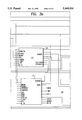
- FIG. 1 is a block diagram showing the interconnection of the major components of a time division multiplex (TDM) system of the invention
- FIG. 2 (represented as FIGS. 2A, 2B and 2C, on three separate sheets) is a block diagram showing a preferred distributed frame processor (DFP) utilized in the channel cards of the invention;
- DFP distributed frame processor
- FIG. 3 and 3A-3C are a block diagram showing a preferred system communication manager (SCM) utilized in the common control module of the invention.
- SCM system communication manager
- FIG. 4 is a timing diagram of a sample system overhead frame (SOF) structure for use with the present invention.
- SOF sample system overhead frame
- TDM system 100 includes a system clock bus 102, a system synchronization bus 104, a high speed bit serial data bus 106, a line interface module 108, a common control module 110, and a plurality of channel modules 112, 114, . . . 116.
- Each of the modules 108, 110, 112, 114 . . . , 116 are coupled to the clock, synch, and data buses, with the common control module 110 generating the synch signal 104 from the clock signal 102, and providing the synch signal to the other modules.
- the high speed bit serial data bus 106 is preferably implemented using wire-ORed FUTUREBUS tranceivers.
- each of the line interface and channel modules generally comprises a distributed frame processor (DFP) 118, 120, 122, 124, . . . 126, (which is discussed hereinafter in detail with reference to FIG. 2) and an interface 128, 130, 132, 134, . . . 136.
- DFP distributed frame processor
- the line interface module uses the line interface 128 to interface with an aggregate link 144
- the channel modules utilize the channel interfaces 132, 134, . . . 136 to interface to data channels 138, 140, . . . 142.
- the TDM system 110 combines a number of input signals, exemplified by channel data signals 138, 140 and 142, into an output aggregate signal 144, and vice versa.
- one of the paths of the signals is through channel modules 112, 114, and 116 respectively, onto high speed data bus 106, and out via the line interface module 108.
- the other path is through line interface module 108, onto the high speed data bus 106, and out via the channel modules 112, 114, . . . 116.
- Traffic on the data bus 106 which governs the transfer of data is controlled by frame information which is determined by the common control module 110.
- the frame information relating when each of modules 112, 114 and 116 are to place their data onto data bus 106 is computed, and initially stored, within module 110. It is subsequently distributed to all of the channel and line interface modules 108, 112, 114 . . . 116 within TDM 100.
- the frame information within common control module 110 specifies each specific time slice during the frame when each source of bus data, such as channel modules 112, 114, 116 or line interface module 108 can either read or write from/to data bus 106.
- 9,216,000 bits per second may be written onto the data bus and read off the data bus, and thus the frame will control 9,216,000 time slices per second.
- 512 KHz of the 9.216 MHz is used for a "manual mechanism" which relates to transmitting the frame, and an additional 512 KHz of the 9.216 MHz is used for the system overhead frame (SOF).
- SOF system overhead frame
- the 8.192 MHz remainder of the 9.216 MHz is used for the channel data.
- the 8.192 MHz remainder permits a 4.096 MHz bandwidth in each direction; i.e., 4,096,000 bits per second can be received by the channel cards from the data channels, multiplexed on the high speed bus, and output on a plurality of aggregate links, while an additional 4,096,000 bits per second can be received by typically a plurality of line interface modules from a plurality of aggregate links, and output via the channel modules (i.e., demultiplexed) to the data channels.
- the frame which controls the placing of data onto and the taking of data off of the high speed data bus 106 is determined by the common control module 110.
- the channel modules are capable of making those decisions independently.
- the on-bus and off-bus frames of the TDM system are distributed by the system control module 120 to the distributed frame processors (DFPs) 118, 122, 124, . . . 126 of the channel and line interface modules where the frames are stored and used to control access to bus 106 independently of the control module 110.
- the distribution of the frames to the DFPs is accomplished via the placement of frame information onto the data bus 106.
- the frame data is the only data placed on the data bus, and is placed on the bus at a rate of 512 KHz in predetermined "locations" of the 9.216 MHz signal.
- locations of the 9.216 MHz signal are also reserved for framing information even when channel data (up to 8.192 MHz) is being multiplexed on the fast data bus 106.
- the frames which are transmitted to the DFPs by the SCM are received and decoded (if necessary) by the distributed frame processors (DFP) 118, 122, 124 . . . , 126 in modules 108, 112, 114, and 116 respectively.
- the frames are then stored in RAM associated with each of the DFPs. Having received the frame information, and based on the synch signals received on bus 104, the DFP's 122, 124 . . . 126 output the data received via the channel interfaces 132, 134 and 136 on the bus 106 at times specified by the on-bus frame structure without further intervention from the common control module 110.
- the fast clock 102 which is distributed to all the DFP's as well as the SCM 120 provides mechanism for assuring that all DFP's in the system have a common time frame for placing data onto the bus (e.g., immediately following the rising edge of the clock).
- the synch bus 104 provides a synchronization signal which permits all of the modules such as modules 108, 110, 112, 114, . . . 116 to initiate an event (e.g., the start of a frame) concurrently.
- the bus 106 is configured as a single conductor which interconnects each printed circuit board of the TDM 100 such as, for example, channel modules 112, 114 . . . 116, line interface module 108, and common control module 110.
- the two separate data frames e.g., the "onto bus” data frame, and the "off of bus” data frame
- the fast bus 8.192 MHz
- each channel module or line interface card of the system receives all data which is placed on the bus.
- the modules only process the data when the receive (off-bus) frame processed by the card indicates that the data is intended for that particular card. Because the bus is bidirectional, the channel module cards could be arranged to look at information at only half the 8.192 data rate, with the line interface card and common control card looking at the other half of the data. Also, if desired, and as described in more detail hereinafter, the system can be arranged so that each card is assigned to a particular aggregate, such that, e.g., only one-half of that half of the bits on the bus could possibly be intended for any particular card. As described below, this allows each card to synchronize to one of two possible incoming (and outgoing) frames under software control.
- the card would use a lower rate frame (e.g., 2.048 MHz) to determine whether the channel data on the bus is intended for it. It will be appreciated, however, that at the same time, separate mechanisms are used by the card to determine whether to put or take manual mechanism or system overhead bits onto or off of the fast bus, as described in more detail below.
- a lower rate frame e.g. 2.048 MHz
- the DFPs serve to interface the data coming from bus 106 onto the channel interface units 132, 134, . . . 136 or line interface unit 128 or vice versa.
- DFP 118 in module 108 interfaces with line interface unit 128.
- the function of DFP 118 is to process the data to or from bus 106 and prepare it for processing by the line interface unit 128.
- DFPs 122, 124, and 126 work with channel interfaces 132, 134 and 136 respectively, which are associated with channels 138, 140 and 142.
- a local "busy bus" 146 is provided for each module to connect the channel interface (e.g., 136) to its associated DFP (e.g. 126).
- an exemplary DFP 122 (the other DFPs being the same) of the present invention may be broken down into several functions or subparts such as a mode control 202, a manual mechanism 204, a serial data interface 206, a test unit 208, a framer 210, a status unit 212, a scheduler 214, a synch unit 216, a communications (COMMS) unit 218, and an external module interface (EMI) 220.
- a mode control 202 such as a mode control 202, a manual mechanism 204, a serial data interface 206, a test unit 208, a framer 210, a status unit 212, a scheduler 214, a synch unit 216, a communications (COMMS) unit 218, and an external module interface (EMI) 220.
- a mode control 202 such as a mode control 202, a manual mechanism 204, a serial data interface 206, a test unit 208, a framer 210, a status unit 212
- the mode control block 202 stores the operating mode, configuration and control of DFP 200.
- the mode control block contains registers which are written and read by the SCM 120 of the common control module 110 in order to control the operating mode and configuration of the DFP 200.
- the mode control block 202 includes registers for setting frame pointers, setting the group number of the DFP, setting the soft address of the DFP, setting bit type, turning frames on or off, setting the synch mode, and setting the test registers of the DFP.
- the manual mechanism 204 implements a hardware protocol with the SCM 120 to transfer sixteen bit words between the processor 130 of the SCM and the DFP of the channel module.
- the manual mechanism is assigned a bandwidth of 512 KHz such that one bit in eighteen transmitted on data bus 106 is used for this data transfer.
- the transfer protocol consists of forty bit fixed length packets which includes sixteen bits of data and twenty-four bits of address information. Because of the twenty-four bits of address information is provided in the manual mechanism coding scheme, access to any and all DFP's in a system may be accessed with a single command. It will be appreciated that each module obtains its address based on its physical location along the backplane. It will also be appreciated that the "manual mechanism" is the mechanism utilized in providing frame information to the DFPs during initialization of the system. Additional details of the manual mechanism will be described below with reference to a description of the SCM 120 and FIG. 3.
- the serial data interface 206 provides an interface between the high speed data bus 106 and the internals of the DFP.
- the functions performed in interface 206 are timing alignment, data readback and data loopback.
- Data readback compares data written to and read from the bus for test purposes while data loopback aids in fault diagnosis at the field replaceable unit level.
- the test unit 208 of the DFP allows the DFP to be operated in a test mode.
- the test block redefines several I/O pins of the DFP to allow quick access to its internal registers.
- the test unit is used during production test only and is not intended for use during normal operation of the device.
- the framer 210 reads frame instructions from an external Frame RAM 250, and if necessary decodes those instructions.
- the framer 210 also executes the instructions contained in the system overhead frame (SOF) as will be discussed in more detail hereinafter with respect to FIG. 4.
- SOF system overhead frame
- a bandwidth of 512 KHz one in eighteen bits of the fast data bus
- the framer 210 maintains the necessary pointers to execute multi-tiered frames as described in previously incorporated U.S. Pat. No. 4,881,224 to Bains.
- the framer 210 contains two independent execution units. One is used to drive the payload data process (data to/from a remote destination, outside of TDM 100) while the other is used for the SOF (local to the TDM 100).
- the payload data is formatted in such a way that the aggregate data stream is compatible with the structure of well known aggregate signals.
- This payload data frame is usually referred to as the Group Frame.
- the SOF uses one timeslot in eighteen of the fast bit serial data bus to transfer information to/from common control module 110. This one bit in eighteen is separate and distinct from the structure used by the "manual mechanism".
- the Group Frame is a 3-tier frame used to carry payload data to/from a remote node.
- the Group Frame must include some bandwidth for synchronization (SYNCH) and internodal communications (COMMS).
- SYNCH synchronization
- COMMS internodal communications
- the 3-tier frame is used as a mechanism to reduce the amount of RAM required to store the description of the frame. For example, a 2.048 Mbps aggregate, described by a frame repeating at 100 Hz would require a frame length of 2,048,000/100, or 20,480 frame instructions.
- the 3-tier mechanism Using the 3-tier mechanism, however, the storage requirement is reduced to less than 4000 frame instructions (worst case), and typically much less than that.
- the System Overhead Frame (SOF), an example of which is shown in FIG. 4, is intended to be used for those operations which happen on a regular schedule.
- the common control processor creates the SOF which is appropriate for its current configuration in order to automatically collect status, alarms, and to distribute slow control information.
- the SOF provides a convenient manner for the common module to communicate to both intelligent (e.g., modules containing a microprocessor) and non-intelligent modules on the shelf.
- the status unit 212 continually collects status information from the other blocks within the DFP, and transfers the status information to the SCM 120 during the manual mechanism bandwidth and/or the system overhead bandwidth of the frame. Information needed by the processor 130 on a regular basis is transferred during each SOF frame. Additional information specifically requested by the processor 130 of the common control unit 110 is also gathered by the status unit 212 and transferred during the manual mechanism.
- the scheduler 214 is used for internal scheduling of the DFP. More particularly, the DFP has various functions which utilize the busy bus 146 which is internal to the channel module. The highest priority function is transmitting data onto the fast bus 106, whether group frame data or SOF data. The second priority function is receiving data off of the fast bus 106; again whether group frame data or SOF data. The third priority function is the manual mechanism. To properly align data onto the fast bus 106, the DFP requires a substantial internal processing pipeline. Because of this pipeline, requests for use of the busy bus by the various blocks of the DFP may coincide. The scheduler 214 ensures that each block has access to the busy bus 146 and that no requests are lost.
- the synch block 216 provides the mechanism necessary for achieving and maintaining synchronization between the DFP and a remote node.
- Five mechanisms are implemented by the synch block.
- a first mechanism is the generation and transmission of a synch pattern.
- a second mechanism is the "receive synch monitor”.
- the receive synch monitor monitors the synch bits in the frame. The synch bits received are compared with those expected, and errors are counted. The count of the errors can be read by the common control processor to determine the number of synch errors during a period of time.
- a third mechanism implemented by the synch block 216 is a "receive synch search". In a receive synch search if a specified error rate is exceeded, a "frame slip" command is issued to the framer 210.
- the fourth mechanism is a "frame offset calculation” where the synch block 216 computes the actual offset (# of bits) between the transmit and receive frames.
- the fifth mechanism is the "receive offset force”. In the “receive offset force” mechanism, when one DFP in the system calculates a frame offset, software in the receive offset force mechanism loads this offset into the other DFPs to instantly force them "in synch”.
- the control processor 130 of the common control module 110 must have inter-nodal communication paths open to all remote nodes coupled to the TDM 100. Since it is impractical for the processor 130 to execute several Group Frames (one for each destination) and extract the associated inter-nodal communications, the COMMS unit 218 is provided within the DFP. In particular, one DFP associated with each remote destination is designated as the comms processor.
- the comms unit 218 performs two primary functions. First, the comms unit 218 receives communication bits located in the Group Frame from the remote destination, and stores them temporarily in a FIFO buffer. The received communication bits are then sent to the processor 130 in the system overhead frame (SOF). Second, communication bits of the local SOF frame are received by the comms unit 218 and are stored temporarily in a FIFO. Then, those communication bits are sent to the remote destination via the Group Frame.
- the comms unit 218 of the DFP obtains communications information from an incoming Group Frame and inserts communications information into an outgoing Group Frame instead of the common control module, and sends and receives desired communications information to and from the common control module during the system overhead frame. This relieves the common control module from dealing with the Group Frames directly.
- the DFPs act to transfer communication information from each of the associated Group Frames into the System Overhead Frame to be processed by processor 130. The same is also true for the opposite direction.
- the SCM 120 generally performs two major groups of functions: those associated with the manual mechanism; and those associated with the system overhead frame for support of the various communication mechanisms.
- the SCM 120 generally includes a timing generator 302, a manual mechanism 304, a serial data interface 306, a system overhead frame 308, a processor interface 310, a byte storage block 312, a communications interface block 314, and a status and configuration block 316.
- the SCM 120 as seen in FIG. 3 is coupled to the fast clock bus 102, the synch bus 104 and the data bus 106, and also interfaces with the common control processor 130.
- the common control processor utilizes various SCM communication mechanisms to configure and collect status from the other modules in the TDM 100 system and to communicate with remote TDM systems as described below.
- the timing generator block 302 of the SCM functions to generate the synchronization signal which is placed on the synch bus 104.
- the SCM 120 receives the 9.216 MHz clock from the fast clock bus 102 and produces a 50 Hz synch clock signal therefrom by dividing down the fast clock by 184,320.
- the synch clock is used to identify the manual mechanism time slots on data bus 106 (by setting a counter which produces a manual mechanism indication every eighteenth time slot of the fast bus), and may also be used to identify the system overhead frame timeslots if those are regularly placed in the 9.216 MHz clock bandwidth.
- the synch pulse may be used to align on-bus and off-bus alignment.
- the DFPs 118, 122, 124, . . . 126 in the system time synchronize themselves to the bus synch generated by the timing generator block of the SCM 120.
- the manual mechanism 304 of the SCM is intended to be used for those operations such as testing, configuration, and detailed status reporting which do not happen with any regularity.
- a flexible addressing scheme allows individual cards or any group of cards in a typical TDM 100 to be accessed for those purposes.
- the manual mechanism 304 offers several operating modes to the common control processor 130 for generating packets of information.
- a single module such as a line interface module 108 can be addressed by its physical slot number.
- one or more registers on interface module 108 can be sequentially accessed for either read or write operations.
- a variation of this mode allows the same register on multiple cards, such as channel module 112, to be sequentially accessed.
- the next level of addressing allows any collection of cards to be accessed simultaneously.
- Two DFP registers located in a DFP are accessible via one of the simpler manual mechanism modes, and allow each DFP in the TDM system to be addressed as part of a sub-group or collection (as discussed above with regard to the DFP off-bus frame rates).
- the “group” address refers to the collection of cards which belong to a particular aggregate and permits the common control module to talk to every card in the same group at the same time.
- the soft address is another way of grouping cards even though they may be associated with different aggregates. For example, all of the channel module cards may be provided with the same soft address.
- the soft address has the specific purpose for supporting DFP frame downloads (as discussed in more detail hereinafter), but it can also be used for any general purpose grouping.
- the manual mechanism is contained in MAN MECH Block 304 of the SCM 120. It is implemented as a forty bit packet containing a 24 bit header and a 16 bit data field.
- the generation of packets is accomplished by the common control processor 130 initializing SCM registers and setting an enable bit.
- the SCM can be configured to transfer multiple packets. Once running, the SCM will solicit microprocessor 130 every seventy-eight microseconds for data to transfer. To unburden the microprocessor from supplying the data for each packet transfer, the necessary controls have been added to the SCM to work in conjunction with a direct memory access arrangement.
- a special mode of operation allows an efficient downloading of the DFP frames. In this mode, the common control processor 130 can download one DFP frame to modules such as 108, 112, 114, . . . 116 in the same group simultaneously. Each DFP can customize the frame for its own use.
- the preferred forty bit manual mechanism packet is broken into a twenty-four bit header and a sixteen bit data field.
- the forty bit manual mechanism header is preferably set up as follows:
- the access type identifies how all of the DFPs in TDM 100 will be addressed as discussed above.
- the individual access type (000) uses the physical slot address; the group access (group address--001) identifies all cards in a compatible type group (aggregate); the soft access (soft address--010) allows cards with the same configuration to be grouped; and global access (011) allows all cards in the shelf to be accessed simultaneously.
- the "Transfer Mode" of the manual mechanism data field is defined by the combination of the bits in the INT/EXT and FR fields of the manual mechanism header as defined above, where the FR bit is set to a value one (i.e., FR--DFP Frame RAM Download), and where "Ext” defines that the register being accessed is external to the DFP, while “Int” defines that the register being accessed is internal to the DFP.
- the DFP frame RAM download algorithm is supported mostly by the DFP with the SCM providing a special download packet.
- the following pseudo-code is implemented by the DFP and is presented here for clarity of the mechanism.
- serial data interface block 306 is provided to interface the SCM with the future bus drivers of the fast data bus.
- buffers for storing SOF and Manual Mechanism bits are provided within the block, as well as the necessary interface and timing hardware.
- the processor interface 310 of the SCM 120 is designed to operate preferably with a Motorola 68000 series microprocessor. Thus, the processor interface 310 provides the microprocessor with the ability to access all of the SCM's configuration and status registers.
- the byte storage block 312 provides an interface between the SCM 120 and the processor 130 via external RAM 350 for supporting "slow controls” and "status summaries” instructions.
- the "slow controls” instructions effectively pass EIA RS-232 leads (RTS, CTS, Data Set Ready, etc.) to a remote device coupled to the multiplexer, while the "status summaries” include events which are used to interrupt the processor and generate an alarm, such as the number of synch errors, watchdog expirations, frame swaps, hardware failure, unconfigured/configured indications, and in-slot/out-of-slot indications.
- both of these "slow controls” and "status summaries” instructions utilize a byte communication mechanism.
- the external RAM 350 is situated such that it may be accessed by both the byte storage block 312 and a processor 130.
- the slow control instructions allow locations in RAM to be read and shifted out to a DFP. These locations in RAM are shifted into the DFP and placed onto the busy bus of the channel control module as a byte.
- the reverse operation is performed for writing a slow control byte to the RAM.
- the frame index byte is used as an offset into the RAM allowing for a maximum of two hundred fifty-six slow controls to be stored.
- the status summary instruction unidirectional and is used for collecting status from each card in TDM 100. The status, as it is collected, is compared to a mask stored in the frame RAM (written there by software) for generating an interrupt to the processor 130. This allows important events to be acted upon immediately.
- the status byte is then written to a specific block of RAM and indexed by the frame index byte.
- the communications block 314 provides a multiplexed serial data interface to the processor 130 of the common control module for supporting supervisory communications and "inter-module message mechanism” (IMM) instructions.
- the IMM instructions are basically communications between "intelligent" processors on different boards of the multiplexer 100.
- a line interface module might have a microprocessor controlling various aspects of its functioning, and that it is desirable for that microprocessor to be able to communicate with the SCM microprocessor.
- the inter-module message mechanism (IMM) is provided for that purpose.
- the IMM is a multi-bit instruction which when read from the Frame RAM will cause the SOF block to repeat the instruction eight times. This will reduce the amount of Frame RAM required to store a frame.
- the communications block 314 places an eight bit frame index (the byte following the frame instruction in the frame RAM) onto the communications block 314 address bus (which is local to the microprocessor) to identify which serial channel is to be accessed. Therefore, this mechanism allows for the addressing of two hundred fifty-six serial communications channels.
- frame index the byte following the frame instruction in the frame RAM
- address bus which is local to the microprocessor
- the status and configuration block 316 stores the present status of SCM 300.
- the second primary function of the common control card is to execute the system overhead frame (SOF).
- SOF structure (a first example of which is shown in FIG. 4) is intended to be used for those operations which are performed on a regular schedule.
- the common control processor 130 creates the system overhead frame which is appropriate for its current configuration.
- the SOF preferably has a two-tier frame structure which supports supervisory communications, inter-module messages, slow controls, and automatic collection of status information and alarms as described above.
- the SOF block 308 of FIG. 3 provides the mechanism for conducting the SOF frame. Essentially, the byte storage 312, the communications block 314, and the serial data interface block 306 have data which must be moved. The SOF block 308 is coupled to those blocks and instructs those blocks as to how and when to move the data.
- the SOF block 308 reads an eight bit frame instruction from the RAM 350 and an eight bit index from the frame RAM 350 at a rate of 512 KHz.
- the eight bit overhead frame instruction identifies which communication mechanism to operate on while also providing branching information for fetching the next instruction.
- the eight bit overhead frame instruction is preferably contructed as follows:
- the frame indicator bit which is also called the "system overhead bit” allows the SCM to broadcast which of the frames it is currently running.
- FIB frame indicator bit
- the use of the SOF is further detailed in FIG. 4.
- the cycles of the fast clock 102 are seen, and the synch bus 404 is shown providing a synch signal at a 50 Hz rate.
- the system overhead frame is shown to be located in every eighteenth location (e.g., S13) of the fast clock bandwidth, with the S13 bits forming the SOF structure.
- the first eight bits (byte) provides a status summary byte from channel 1.
- the second and third bytes (bits C9-C16 and C17-C24) define status symmary bytes from channel 2 and from the line card.
- Bits C25, C26, C27, and C28 are used as serial communications bits (supervisory comms) to the line card, from the line card, to a redundant common card, and from a redundant common card respectively.
- Bits C29-C36 are then used as a control byte (slow controls) from channel 1; bits C37-44 are used as a control byte to channel 1; bits C45-52 are used as a control byte from channel 2; bits C53-60 are used as a control byte to channel 2; bits C61-68 are used as a control byte from the line card; and bits C69-76 are used as a control byte to the line card.
- a second illustrative example of an SOF frame is as follows:
- Channels 1 and 2 of the example are typical of overhead for a data channel card (channel modules), while channel 3 is typical of overhead for a line interface module.
- the composite frame would appear as follows:
- a "*" indicates that an instruction is repeated eight times. Also, it will be appreciated that the frame instruction and frame index are indicated in hexadecimal code (Ox), while the end flag is bit 0 of the system overhead frame instruction and the next instruction is bit 1 of the SOF instruction.
Abstract
Description
______________________________________
Manual Mechanism 24-bit Header
          Size
Field Name
          (bits) Definitions
______________________________________
Packet Type
          2      00 - Normal
                 11 - Null
Access Type
          3      000 - Individual
                 001 - Group
                 010 - Soft
                 011 - Global
INT/EXT   1      0 - The register being addressed is
                 external to the DFP.
                 1 - The register being addressed is
                 internal to the DFP.
RW        1      0 - The packet contains data to be
                 written
                 1 - The addressed card will provide
                 data
FR        1      0 - Normal
                 1 - DFP Frame RAM Download/Upload
Access Address
          6      Provides the address of the DFP to
                 receive the packet. This can be
                 the physical slot, group or soft
                 address.
Register  8      Provides the address of the
Address          register to be accessed.
NU        2      Not Used
______________________________________
______________________________________
Manual Mechanism 16-bit Data Field
         Size   Transfer
Field Name
         (bits) Mode     Definitions
______________________________________
Data (LSB)
         8      Ext      BUSY BUS Data Byte (D7-D0)
                Int      DFP Lower Byte of Word
                FR       Frame RAM Data Byte
Soft Address
         6      Ext      Not used
                Int      Part of the Upper Data
                         Byte (D13-D8)
                FR       Soft Address used in
                         download algorithm
Override 1      Ext      Not used
                Int      Part of the Upper Data
                         Byte (D14)
                FR       0 - Normal download algorithm
                         1 - Write the data byte to
                         the Frame RAM without
                         modification.
Bit/Byte 1      Ext      Not used
                Int      Part of the Upper Data
                         Byte (D15)
                FR       Defines the type of
                         Instruction
                         0 - Bit
                         1 - Byte
______________________________________
______________________________________
if (  Packet Type = Normal
  .AND. Transfer Mode = Frame RAM
  .AND. RW = Write
  .AND. Access Type = Group
  .AND. Access Address = Group Address)
then
  if (Override = 0)
   then
  {
   if (Packet Soft Address = Configured Soft Address)
   then
   {
    Write Packet Data to Frame RAM
   }
   else
   {
    Change the Packet Data to a NOP instruction
7            6     5     4     3   2   1   0
Bit/Byte     0     0     0   D3  D2  D1  D0
    D3-D0 = Lower nibble of Packet Data
   }
  }
  else
  {
   Write Packet Data to Frame RAM
  }
}
______________________________________
______________________________________ bit 0 EOF indicator 0 - normal 1 - end offrame bit 1 Next instruction 0 - primary next 1 - secondarynext bit 2 Transfer type 0 - off bus 1 - on bus bits 7-3 Information field 00000 bit NOP 00001 comms bit 00010 system overhead frame indicator (FIB) 00011 bit reserved for future use . . . 00111 bit reserved for future use 01000 IMM bit 01001 bit reserved for future use . . . 01111 bit reserved for future use 10000 byte NOP 10001 slow control byte 10010 status summary byte 10011 byte reserved for future use 10100 byte reserved for future use 10101 slow control byte - channel B of dual or quad channel 10110 byte reserved for future use 10111 byte reserved for future use 11000 byte reserved for future use 11001 slow control byte - channel C of quad channel 11010 byte reserved for future use 11011 byte reserved for future use 11100 byte reserved for future use 11101 slow control byte - channel D of quad channel 11110 byte reserved for future use 11111 byte reserved for future use ______________________________________
______________________________________
frame                     next end  frame frame
index  opcode      index  instr
                               flag inst  index
______________________________________
pri 0      COMMS    ON   CH1  sec       OxOe  Ox01
sec 0      COMMS    ON   CH1  pri       Ox0c  Ox01
pri 1      COMMS    OFF  CH1  pri       OxO8  Ox01
pri 2      COMMS    ON   CH2  pri       Ox0c  OxO2
pri 3      COMMS    OFF  CH2  pri       Ox08  OxO2
pri 4      IMM      ON   CH3  pri       Ox44  OxO3
*:    :    :        :    :         :    :
pri 5      IMM      OFF  CH3  pri       Ox4O  OxO3
*:    :    :        :    :         :    :
pri 6      SC       ON   CH1  pri       Ox8c  Ox01
*:    :    :        :    :         :    :
pri 7      SC       OFF  CH1  pri       Ox88  Ox01
*:    :    :        :    :         :    :
pri 8      SC       ON   CH2  sec       Ox8e  OxO2
*:    :    :        :    :         :    :
sec 1      SS       ON   CH1  pri       Ox94  Ox01
*:    :    :        :    :         :    :
pri 9      SC       OFF  CH2  pri       Ox88  Ox02
*:    :    :        :    :         :    :
pri 10     Bit      NOP       pri       Ox00  Ox00
pri 11     Bit      NOP       pri       Ox00  Ox00
pri 12     Bit      NOP       pri  eof  Ox00  Ox00
pri 0      COMMS    ON   CH1  sec       OxOe  Ox01
sec 2      COMMS    ON   CH2  pri       Ox0c  OxO2
pri 1      COMMS    OFF  CH1  pri       OxO8  Ox01
pri 2      COMMS    ON   CH2  pri       Ox0c  OxO2
pri 3      COMMS    OFF  CH2  pri       Oxos  OxO2
pri 4      IMM      ON   CH3  pri       Ox44  OxO3
*:    :    :        :    :         :    :
pri 5      IMM      OFF  CH3  pri       Ox4O  OxO3
*:    :    :        :    :         :    :
pri 6      SC       ON   CH1  pri       Ox8c  Ox01
*:    :    :        :    :         :    :
pri 7      SC       OFF  CH1  pri       Ox88  Ox01
*:    :    :        :    :         :    :
pri 8      SC       ON   CH2  sec       Ox8e  OxO2
*:    :    :        :    :         :    :
sec 3      SS       ON   CH3  pri       Ox94  OxO3
*:    :    :        :    :         :    :
pri 9      SC       OFF  CH2  pri       Ox88  OxO2
*:    :    :        :    :         :    :
pri 10     Bit      NOP       pri       Ox00  Ox00
pri 11     Bit      NOP       pri       Ox00  Ox00
pri 12     Bit      NOP       pri  eof  Ox00  Ox00
pri 0      COMMS    ON   CH1  sec       OxOe  Ox01
sec 4      COMMS    OFF  CH1  pri       Ox08  Ox01
pri 1      COMMS    OFF  CH1  pri       Ox08  Ox01
pri 2      COMMS    ON   CH2  pri       Ox0c  OxO2
pri 3      COMMS    OFF  CH2  pri       Ox08  OxO2
pri 4      IMM      ON   CH3  pri       Ox44  OxO3
*:    :    :        :    :         :    :
pri 5      IMM      OFF  CH3  pri       Ox4O  OxO3
*:    ;    :        :    :         :    :
pri 6      SC       ON   CH1  pri       Ox8c  Ox01
*:    :    :        :    :         :    :
pri 7      SC       OFF  CH1  pri       Ox88  Ox01
*:    :    :        :    :         :    :
pri 8      SC       ON   CH2  sec       Ox8e  OxO2
*:    :    :        :    :         :    :
sec 5      SS       ON   CH2  pri       Ox94  OxO2
*:    :    :        :    :         :    :
pri 9      SC       OFF  CH2  pri       Ox88  OxO2
*:    :    :        :    :         :    :
pri 10     Bit      NOP       pri       Ox00  Ox00
pri 11     Bit      NOP       pri       Ox00  Ox00
pri 12     Bit      NOP       pri  eof  Ox00  Ox00
pri 0      COMMS    ON   CH1  sec       OxOe  Ox01
sec 6      COMMS    OFF  CH2  pri       Ox08  OxO2
pri 1      COMMS    OFF  CH1  pri       Ox08  Ox01
pri 2      COMMS    ON   CH2  pri       Ox0c  OxO2
pri 3      COMMS    OFF  CH2  pri       OxO8  OxO2
pri 4      IMM      ON   CH3  pri       Ox44  OxO3
*:    :    :        :    :         :    :
pri 5      IMM      OFF  CH3  pri       Ox4O  OxO3
*:    :    :        :    :         :    :
pri 6      SC       ON   CH1  pri             Ox01
*:    :    :        :    :         :    :
pri 7      SC       OFF  CH1  pri       Ox88  Ox01
*:    :    :        :    :         :    :
pri 8      SC       ON   CH2  sec       Ox8e  OxO2
*:    :    :        :    :         :    :
sec 7      Byte     NOP       pri       Ox00  Ox00
*:    :    :        :    :         :    :
pri 9      SC       OFF  CH2  pri       Ox88  OxO2
*:    :    :        :    :         :    :
pri 10     Bit      NOP       pri       Ox00  Ox00
pri 11     Bit      NOP       pri       Ox00  Ox00
pri 12     Bit      NOP       pri  eof  Ox00  Ox00
pri 0      COMMS    ON   CH1  sec       OxOe  Ox01
sec 8      FIB      ON        pri       Ox14  Ox00
pri 1      COMMS    OFF  CH1  pri       Ox08  Ox01
pri 2      COMMS    ON   CH2  pri       Ox0c  OxO2
pri 3      COMMS    OFF  CH2  pri       Ox08  OxO2
pri 4      IMM      ON   CH3  pri       Ox44  OxO3
*:    :    :        :    :         :    :
pri 5      IMM      OFF  CH3  pri       Ox4O  OxO3
*:    :    :        :    :         :    :
pri 6      SC       ON   CH1  pri       Ox8c  Ox01
*:    :    :        :    :         :    :
pri 7      SC       OFF  CH1  pri       Ox88  Ox01
*:    :    :        :    :         :    :
pri 8      SC       ON   CH2  sec       Ox8e  OxO2
*:    :    :        :    :         :    :
sec 9      Byte     NOP       pri  eof  Ox00  Ox00
*:    :    :        :    :         :    :
pri 9      SC       OFF  CH2  pri       Ox88  Ox02
*:    :    :        :    :         :    :
pri 10     Bit      NOP       pri       Ox00  Ox00
pri 11     Bit      NOP       pri       Ox00  Ox00
pri 12     Bit      NOP       pri  eof  Ox00  Ox00
______________________________________
______________________________________
Primary frame
frame                    next end  frame  frame
index opcode      index  instr
                              flag inst   index
______________________________________
pri0  COMMS    ON     CH1  sec       Ox0e   Ox01
pri1  COMMS    OFF    CH1  pri       Ox08   Ox01
pri2  COMMS    ON     CH2  pri       Ox0c   Ox02
pri3  COMMS    OFF    CH2  pri       Ox08   Ox02
pri4  IMM      ON     CH3  pri       Ox44   Ox03
pri5  IMM      OFF    CH3  pri       Ox40   Ox03
pri0  SC       ON     CH1  pri       Ox8c   Ox01
pri7  SC       OFF    CH1  pri       Ox88   Ox01
pri8  SC       ON     CH2  sec       Ox8e   Ox02
pri9  SC       OFF    CH2  pri       Ox88   Ox02
pri10 Bit      NOP         pri       Ox00   Ox00
pri11 Bit      NOP         pri       Ox00   Ox00
pril2 Bit      NOP         pri  eof  Ox00   Ox00
______________________________________
Secondary frame
frame                    next end  frame  frame
index opcode      index  frm  flag inst   index
______________________________________
sec 0 COMMS    ON     CH1  pri       Ox0c   Ox01
sec 1 SS       ON     CH1  pri       Ox94   Ox01
sec 2 COMMS    ON     CH2  pri       Ox0c   Ox02
sec 3 SS       ON     CH3  pri       Ox94   Ox03
sec 4 COMMS    OFF    CH1  pri       Ox08   Ox01
sec 5 SS       ON     CH2  pri       Ox94   Ox02
sec 6 COMMS    OFF    CH2  pri       Ox08   Ox02
sec 7 Byte     NOP         pri       Ox00   Ox00
sec 8 FIB      ON          pri       Oxl4   Ox00
sec 9 Byte     NOP         pri  eof  Ox00   Ox00
______________________________________
Claims (20)
Priority Applications (5)
| Application Number | Priority Date | Filing Date | Title |
|---|---|---|---|
| US08/007,074 US5469434A (en) | 1993-01-21 | 1993-01-21 | Distributed frame processing for time division multiplexing |
| PCT/US1994/000734 WO1994017612A1 (en) | 1993-01-21 | 1994-01-19 | Distributed frame processing for time division multiplexing |
| AU60921/94A AU677291B2 (en) | 1993-01-21 | 1994-01-19 | Distributed frame processing for time division multiplexing |
| CA002151393A CA2151393A1 (en) | 1993-01-21 | 1994-01-19 | Distributed frame processing for time division multiplexing |
| EP94907275A EP0680677A4 (en) | 1993-01-21 | 1994-01-19 | Distributed frame processing for time division multiplexing. |
Applications Claiming Priority (1)
| Application Number | Priority Date | Filing Date | Title |
|---|---|---|---|
| US08/007,074 US5469434A (en) | 1993-01-21 | 1993-01-21 | Distributed frame processing for time division multiplexing |
Publications (1)
| Publication Number | Publication Date |
|---|---|
| US5469434A true US5469434A (en) | 1995-11-21 |
Family
ID=21724078
Family Applications (1)
| Application Number | Title | Priority Date | Filing Date |
|---|---|---|---|
| US08/007,074 Expired - Fee Related US5469434A (en) | 1993-01-21 | 1993-01-21 | Distributed frame processing for time division multiplexing |
Country Status (5)
| Country | Link |
|---|---|
| US (1) | US5469434A (en) |
| EP (1) | EP0680677A4 (en) |
| AU (1) | AU677291B2 (en) |
| CA (1) | CA2151393A1 (en) |
| WO (1) | WO1994017612A1 (en) |
Cited By (13)
| Publication number | Priority date | Publication date | Assignee | Title |
|---|---|---|---|---|
| US5612954A (en) * | 1994-04-29 | 1997-03-18 | Telefonaktiebolaget Lm Ericsson | Time switch system |
| US5951659A (en) * | 1997-04-07 | 1999-09-14 | Ncr Corporation | Communications-oriented computer system backplane including a PCI input/output bus for transmission of address, data, and control information, and a time-domain multiplexed signal bus (TDMSB) for transmission of high-speed digitized signal information |
| US6115756A (en) * | 1997-06-27 | 2000-09-05 | Sun Microsystems, Inc. | Electro-optically connected multiprocessor and multiring configuration for dynamically allocating time |
| US6154728A (en) * | 1998-04-27 | 2000-11-28 | Lucent Technologies Inc. | Apparatus, method and system for distributed and automatic inventory, status and database creation and control for remote communication sites |
| US20010005862A1 (en) * | 1999-12-22 | 2001-06-28 | Lg Electronics Inc. | Method for down-loading data |
| US20020009097A1 (en) * | 2000-05-26 | 2002-01-24 | Tetsujiro Kondo | Signal processing apparatus |
| US6385208B1 (en) * | 1998-06-02 | 2002-05-07 | Cisco Technology, Inc. | Serial media independent interface |
| US20030002079A1 (en) * | 1998-05-09 | 2003-01-02 | Hartman Susan A. | Recovery of bit-rotated frames during facsimile transmissions in a global system for mobile communications (GSM) network |
| US6631138B1 (en) | 1998-06-02 | 2003-10-07 | Cisco Technology, Inc. | Reduced pin-count 10Base-T MAC to transceiver interface |
| US6947427B1 (en) * | 1999-09-29 | 2005-09-20 | Nec Corporation | Transmission method and network system for accommodating a plurality of kinds of traffic in a common network |
| US6977885B1 (en) * | 1999-08-25 | 2005-12-20 | Hitachi, Ltd. | Packet transmitting and receiving method and apparatus therefor |
| US7031333B1 (en) | 1998-06-02 | 2006-04-18 | Cisco Technology, Inc. | Reduced pin count media independent interface |
| US20130223236A1 (en) * | 2012-02-29 | 2013-08-29 | Hamilton Sundstrand Corporation | Channel interleaved multiplexed databus |
Citations (11)
| Publication number | Priority date | Publication date | Assignee | Title |
|---|---|---|---|---|
| US4653049A (en) * | 1984-07-12 | 1987-03-24 | Nec Corporation | Multidirection multiplex communication systems |
| US4742512A (en) * | 1985-07-19 | 1988-05-03 | Nec Corporation | Multipoint communication system having polling and reservation schemes |
| US4763320A (en) * | 1984-07-06 | 1988-08-09 | Messerschmitt-Bolkow-Blohm Gmbh | Method and arrangement for transmitting data, especially in an aircraft |
| US4787081A (en) * | 1986-01-22 | 1988-11-22 | Stc Plc | Time division multiplex equipment for use in data transmission equipment |
| US4872003A (en) * | 1984-11-30 | 1989-10-03 | Nec Corporation | Serial interface system flexibly applicable to a one-to-plurality connection |
| US4881224A (en) * | 1988-10-19 | 1989-11-14 | General Datacomm, Inc. | Framing algorithm for bit interleaved time division multiplexer |
| US4882730A (en) * | 1986-11-28 | 1989-11-21 | Nec Corporation | TDMA communication system having common time slots for system maintenance |
| US4907222A (en) * | 1988-08-17 | 1990-03-06 | Nuvatec, Inc. | Vehicle multiplex system |
| US5084872A (en) * | 1989-06-19 | 1992-01-28 | Alcatel Business Systems | Interface for transmit and receive mode access to the synchronous transmission medium of a distributed switching network |
| US5144621A (en) * | 1990-09-28 | 1992-09-01 | Nec Corporation | Common bus communication system with reduced interface memories |
| US5177737A (en) * | 1990-01-02 | 1993-01-05 | At&T Bell Laboratories | Multipurpose bus system |
Family Cites Families (1)
| Publication number | Priority date | Publication date | Assignee | Title |
|---|---|---|---|---|
| JP2579963B2 (en) * | 1987-10-26 | 1997-02-12 | シャープ株式会社 | Communication method |
-
1993
- 1993-01-21 US US08/007,074 patent/US5469434A/en not_active Expired - Fee Related
-
1994
- 1994-01-19 EP EP94907275A patent/EP0680677A4/en not_active Withdrawn
- 1994-01-19 AU AU60921/94A patent/AU677291B2/en not_active Ceased
- 1994-01-19 CA CA002151393A patent/CA2151393A1/en not_active Abandoned
- 1994-01-19 WO PCT/US1994/000734 patent/WO1994017612A1/en not_active Application Discontinuation
Patent Citations (11)
| Publication number | Priority date | Publication date | Assignee | Title |
|---|---|---|---|---|
| US4763320A (en) * | 1984-07-06 | 1988-08-09 | Messerschmitt-Bolkow-Blohm Gmbh | Method and arrangement for transmitting data, especially in an aircraft |
| US4653049A (en) * | 1984-07-12 | 1987-03-24 | Nec Corporation | Multidirection multiplex communication systems |
| US4872003A (en) * | 1984-11-30 | 1989-10-03 | Nec Corporation | Serial interface system flexibly applicable to a one-to-plurality connection |
| US4742512A (en) * | 1985-07-19 | 1988-05-03 | Nec Corporation | Multipoint communication system having polling and reservation schemes |
| US4787081A (en) * | 1986-01-22 | 1988-11-22 | Stc Plc | Time division multiplex equipment for use in data transmission equipment |
| US4882730A (en) * | 1986-11-28 | 1989-11-21 | Nec Corporation | TDMA communication system having common time slots for system maintenance |
| US4907222A (en) * | 1988-08-17 | 1990-03-06 | Nuvatec, Inc. | Vehicle multiplex system |
| US4881224A (en) * | 1988-10-19 | 1989-11-14 | General Datacomm, Inc. | Framing algorithm for bit interleaved time division multiplexer |
| US5084872A (en) * | 1989-06-19 | 1992-01-28 | Alcatel Business Systems | Interface for transmit and receive mode access to the synchronous transmission medium of a distributed switching network |
| US5177737A (en) * | 1990-01-02 | 1993-01-05 | At&T Bell Laboratories | Multipurpose bus system |
| US5144621A (en) * | 1990-09-28 | 1992-09-01 | Nec Corporation | Common bus communication system with reduced interface memories |
Non-Patent Citations (2)
| Title |
|---|
| Stallings, Data And Computer Communications, 1988, pp. 42 45, 174 175, and 182 185. * |
| Stallings, Data And Computer Communications, 1988, pp. 42-45, 174-175, and 182-185. |
Cited By (22)
| Publication number | Priority date | Publication date | Assignee | Title |
|---|---|---|---|---|
| US5612954A (en) * | 1994-04-29 | 1997-03-18 | Telefonaktiebolaget Lm Ericsson | Time switch system |
| US5951659A (en) * | 1997-04-07 | 1999-09-14 | Ncr Corporation | Communications-oriented computer system backplane including a PCI input/output bus for transmission of address, data, and control information, and a time-domain multiplexed signal bus (TDMSB) for transmission of high-speed digitized signal information |
| US6385657B1 (en) | 1997-06-27 | 2002-05-07 | Sun Microsystems, Inc. | Chain transaction transfers between ring computer systems coupled by bridge modules |
| US6115756A (en) * | 1997-06-27 | 2000-09-05 | Sun Microsystems, Inc. | Electro-optically connected multiprocessor and multiring configuration for dynamically allocating time |
| US6859844B2 (en) | 1997-06-27 | 2005-02-22 | Sun Microsystems, Inc. | Electro-optically connected multiprocessor configuration including a ring structured shift-register |
| US20020091865A1 (en) * | 1997-06-27 | 2002-07-11 | Sun Microsystems, Inc. | Electro-optically connected multiprocessor configuration |
| US6154728A (en) * | 1998-04-27 | 2000-11-28 | Lucent Technologies Inc. | Apparatus, method and system for distributed and automatic inventory, status and database creation and control for remote communication sites |
| US20030002079A1 (en) * | 1998-05-09 | 2003-01-02 | Hartman Susan A. | Recovery of bit-rotated frames during facsimile transmissions in a global system for mobile communications (GSM) network |
| US6894801B2 (en) * | 1998-05-09 | 2005-05-17 | Intel Corporation | Recovery of bit-rotated frames during facsimile transmissions in a global system for mobile communications (GSM) network |
| US6385208B1 (en) * | 1998-06-02 | 2002-05-07 | Cisco Technology, Inc. | Serial media independent interface |
| US7227869B2 (en) * | 1998-06-02 | 2007-06-05 | Cisco Technology, Inc. | Serial media independent interface |
| US20020126684A1 (en) * | 1998-06-02 | 2002-09-12 | Cisco Technology, Inc. | Serial media independent interface |
| US6631138B1 (en) | 1998-06-02 | 2003-10-07 | Cisco Technology, Inc. | Reduced pin-count 10Base-T MAC to transceiver interface |
| US20070160087A1 (en) * | 1998-06-02 | 2007-07-12 | Cisco Technology, Inc. | Serial media independent interface |
| US7031333B1 (en) | 1998-06-02 | 2006-04-18 | Cisco Technology, Inc. | Reduced pin count media independent interface |
| US6977885B1 (en) * | 1999-08-25 | 2005-12-20 | Hitachi, Ltd. | Packet transmitting and receiving method and apparatus therefor |
| US6947427B1 (en) * | 1999-09-29 | 2005-09-20 | Nec Corporation | Transmission method and network system for accommodating a plurality of kinds of traffic in a common network |
| US20010005862A1 (en) * | 1999-12-22 | 2001-06-28 | Lg Electronics Inc. | Method for down-loading data |
| US20020009097A1 (en) * | 2000-05-26 | 2002-01-24 | Tetsujiro Kondo | Signal processing apparatus |
| US7248599B2 (en) * | 2000-05-26 | 2007-07-24 | Sony Corporation | Signal processing apparatus |
| US20130223236A1 (en) * | 2012-02-29 | 2013-08-29 | Hamilton Sundstrand Corporation | Channel interleaved multiplexed databus |
| US8953463B2 (en) * | 2012-02-29 | 2015-02-10 | Hamilton Sundstrand Corporation | Channel interleaved multiplexed databus |
Also Published As
| Publication number | Publication date |
|---|---|
| CA2151393A1 (en) | 1994-08-04 |
| AU6092194A (en) | 1994-08-15 |
| EP0680677A1 (en) | 1995-11-08 |
| WO1994017612A1 (en) | 1994-08-04 |
| EP0680677A4 (en) | 1998-04-08 |
| AU677291B2 (en) | 1997-04-17 |
Similar Documents
| Publication | Publication Date | Title |
|---|---|---|
| US5615211A (en) | Time division multiplexed backplane with packet mode capability | |
| US5469434A (en) | Distributed frame processing for time division multiplexing | |
| US6275499B1 (en) | OC3 delivery unit; unit controller | |
| US6185630B1 (en) | Device initializing system with programmable array logic configured to cause non-volatile memory to output address and data information to the device in a prescribed sequence | |
| US7460482B2 (en) | Master-slave communications system and method for a network element | |
| US4998249A (en) | Method and system for multiplexing telephone line circuits to highway lines | |
| EP0559090B1 (en) | Network element comprising a cross-connect matrix and a server | |
| US20030043851A1 (en) | Transmit virtual concatenation processor | |
| EP0397197A2 (en) | Synchronous optical transmission system | |
| US7009978B2 (en) | Communications interface for providing a plurality of communication channels to a single port on a processor | |
| WO1990006645A1 (en) | System for cross-connecting high speed digital signals | |
| US5878039A (en) | Bus rate adaptation and time slot assignment circuit for a sonet multiplex system | |
| US20080137674A1 (en) | Data byte load based network byte-timeslot allocation | |
| JP3442180B2 (en) | Add-drop multiplex equipment | |
| CA2357944A1 (en) | Multi-subshelf control system and method for a network element | |
| CA2031785C (en) | Apparatus for programmably accessing and assigning time slots in a time division multiplexed communication system | |
| US6754174B1 (en) | Interface for communications among network elements | |
| US6493346B1 (en) | System for providing conversion of TDM-based frame relay data in a cross-connect matrix to and from ATM data | |
| US6633573B1 (en) | Method and apparatus for generating massive interrupts in random access memory (RAM) | |
| US6208648B1 (en) | Network element and input/output device for a synchronous transmission system | |
| US5768265A (en) | Duplex signal multiplexing system | |
| US7054324B1 (en) | Interface transmitter for communications among network elements | |
| Cisco | Synchronous Data Connections | |
| US6785766B1 (en) | Method and apparatus for servicing massive interrupts in random access memory (RAM) | |
| EP1298867B1 (en) | Master-slave communication system and method for a network element |
Legal Events
| Date | Code | Title | Description |
|---|---|---|---|
| AS | Assignment |
Owner name: GENERAL DATACOMM, INC., CONNECTICUT Free format text: ASSIGNMENT OF ASSIGNORS INTEREST.;ASSIGNORS:KURDZO, JAMES P.;KATZE, ALAN B., JR.;REEL/FRAME:006405/0437 Effective date: 19930120 |
|
| AS | Assignment |
Owner name: TRANSAMERICA BUSINESS CREDIT CORPORATION, AS AGENT Free format text: SECURITY AGREEMENT;ASSIGNOR:GENERAL DATACOMM, INC.;REEL/FRAME:008829/0038 Effective date: 19971022 |
|
| AS | Assignment |
Owner name: FOOTHILL CAPITAL CORPORATION, AS AGENT, CALIFORNIA Free format text: SECURITY INTEREST;ASSIGNORS:GENERAL DATACOMM, INC., A CORP. OF DE;GENERAL DATACOMM INDUSTRIES, INC., A CORP. OF DE;REEL/FRAME:009935/0139 Effective date: 19990514 |
|
| AS | Assignment |
Owner name: GENERAL DATACOMM INDUSTRIES, INC., (DELAWARE CORPO Free format text: RELEASE BY SECURED PARTY;ASSIGNOR:TRANSAMERICA BUSINESS CREDIT CORPORATION, AS AGENT;REEL/FRAME:009942/0001 Effective date: 19990513 Owner name: GENERAL DATACOMM, INC., CONNECTICUT Free format text: RELEASE BY SECURED PARTY;ASSIGNOR:TRANSAMERICA BUSINESS CREDIT CORPORATION, AS AGENT;REEL/FRAME:009942/0001 Effective date: 19990513 |
|
| REMI | Maintenance fee reminder mailed | ||
| LAPS | Lapse for failure to pay maintenance fees | ||
| FP | Lapsed due to failure to pay maintenance fee |
Effective date: 19991121 |
|
| STCH | Information on status: patent discontinuation |
Free format text: PATENT EXPIRED DUE TO NONPAYMENT OF MAINTENANCE FEES UNDER 37 CFR 1.362 |