US5726990A - Multiplexer and demultiplexer - Google Patents

Multiplexer and demultiplexer Download PDF

Info

Publication number
US5726990A
US5726990A US08/629,148 US62914896A US5726990A US 5726990 A US5726990 A US 5726990A US 62914896 A US62914896 A US 62914896A US 5726990 A US5726990 A US 5726990A
Authority
US
United States
Prior art keywords
stage
data
block
variable delay
multiplexer
Prior art date
Legal status (The legal status is an assumption and is not a legal conclusion. Google has not performed a legal analysis and makes no representation as to the accuracy of the status listed.)
Expired - Fee Related
Application number
US08/629,148
Inventor
Masaaki Shimada
Norio Higashisaka
Current Assignee (The listed assignees may be inaccurate. Google has not performed a legal analysis and makes no representation or warranty as to the accuracy of the list.)
Mitsubishi Electric Corp
Original Assignee
Mitsubishi Electric Corp
Priority date (The priority date is an assumption and is not a legal conclusion. Google has not performed a legal analysis and makes no representation as to the accuracy of the date listed.)
Filing date
Publication date
Application filed by Mitsubishi Electric Corp filed Critical Mitsubishi Electric Corp
Assigned to MITSUBISHI DENKI KABUSHIKI KAISHA reassignment MITSUBISHI DENKI KABUSHIKI KAISHA ASSIGNMENT OF ASSIGNORS INTEREST (SEE DOCUMENT FOR DETAILS). Assignors: HIGASHISAKA, NORIO, SHIMADA, MASAAKI
Application granted granted Critical
Publication of US5726990A publication Critical patent/US5726990A/en
Anticipated expiration legal-status Critical
Expired - Fee Related legal-status Critical Current

Links

Images

Classifications

    • HELECTRICITY
    • H03ELECTRONIC CIRCUITRY
    • H03MCODING; DECODING; CODE CONVERSION IN GENERAL
    • H03M9/00Parallel/series conversion or vice versa
    • HELECTRICITY
    • H04ELECTRIC COMMUNICATION TECHNIQUE
    • H04JMULTIPLEX COMMUNICATION
    • H04J3/00Time-division multiplex systems
    • H04J3/02Details
    • H04J3/06Synchronising arrangements
    • H04J3/0635Clock or time synchronisation in a network
    • H04J3/0685Clock or time synchronisation in a node; Intranode synchronisation

Definitions

  • the present invention relates to a multiplexer for converting parallel data to serial data and a demultiplexer for converting serial data to parallel data and, more particularly, to a multiplexer and a demultiplexer used for high-speed operation.
  • FIG. 19 is a circuit diagram illustrating a prior art multiplexer.
  • the m:1 multiplexer block comprises a number of D flip-flops equal to the input parallel data.
  • Reference numeral 4 designates a D flip-flop for timing control.
  • Reference numeral 5a designates a frequency divider that divides the frequency of an input clock signal to produce an output signal having a frequency that is an exact integral submultiple of the input frequency. The integral submultiple depends on the circuit structure of the m:1 MUX block 3a.
  • Reference numeral 60 designates a parallel data input terminal.
  • Reference numeral 61 designates a serial data output terminal.
  • Reference character CLK designates a high-speed clock.
  • Reference numeral 64 designates a high-speed clock input terminal.
  • the prior art multiplexer comprises the output stages S 1 to S n , and the final output stage S n includes the D flip-flop 4 that synchronizes the serial data output from the previous stage S n-1 with the high-speed clock input CLK.
  • the m n-j-1 m:1 MUX blocks 3a in the S j stage are connected to the next stage so that the serial data output from each m:1 MUX block 3a in the S j stage becomes one of the parallel data input to the m:1 MUX block 3a in the next stage or becomes serial data input to the D flip-flop 4 in the S n stage.
  • a plurality of parallel data inputs to the input terminal 60 are successively converted into serial data by the m:1 MUX blocks 3a, and serial data is produced at the S n-1 stage prior to the final stage.
  • This serial data is synchronized with the clock CLK at the final stage S n and output from the output terminal 61 as a serial data output.
  • FIG. 12 is a block diagram for explaining the operating principle of the prior art multiplexer.
  • the multiplexer 200 includes 2:1 MUX blocks 1, 2, and 3 corresponding to the m:1 MUX blocks 3a, 1/2 frequency dividers 5 and 5b corresponding to the frequency dividers 5a, and a D flip-flop 4.
  • Reference character SIG 1 denotes a serial data output from the 2:1 MUX block 3.
  • the multiplexer 200 is a 4:1 multiplexer converting four bit parallel data into serial data, the operating principle is identical even when the bit number of the input parallel data is changed.
  • FIG. 13 is a block diagram illustrating a circuit structure of the 2:1 MUX blocks 1 to 3 shown in FIG. 12.
  • reference numeral 7 designates a D flip-flop
  • numeral 8 designates a D flip-flop with a phase shifter
  • numeral 9 designates a two-input selector. More specifically, the D flip-flop 7 latches the input data and outputs the data synchronously with clocks input to the 2:1 MUX block.
  • the D flip-flop 8 with the phase shifter latches the input data, delays the phase of the data by 1/2 period of the clock input to the 2:1 MUX block, and outputs the data.
  • the two-input selector 9 selects one of the outputs from the D flip-flops 7 and 8 synchronously with a clock signal.
  • the parallel data B input to the D flip-flop 8 is phase-delayed by 1/2 period from the parallel data A input to the D flip-flop 7 when it is input to the selector 9.
  • the parallel data A and the parallel data B are alternatingly selected at intervals equivalent to 1/2 period of the input clock.
  • the 2:1 MUX block converts two bit parallel data into serial data.
  • the operation of the m:1 MUX block 3a shown in FIG. 19 is fundamentally identical to the above-described operation although the number of the D flip-flops and the operating timing of the selector are different. More specifically, in the m:1 MUX block, the number of the D flip-flops is m, and one of the m D flip-flops has no phase shifter. That is, the (m-1) D flip-flops delay the phases of the input clocks by 1/m period, 2/m period, . . . , (m-1)/m period, respectively.
  • the multiplexer 200 comprises the 2:1 MUX blocks 1 to 3, the D flip-flop 4, and the frequency dividers 5 and 5b for dividing the frequency of an input clock to 1/2.
  • the by 2 frequency dividers 5 and 5b produce a clock 1/2 CLK having a frequency equivalent to a half of the frequency of the high-speed clock CLK and a clock 1/4 CLK having a frequency equivalent to a quarter of the high-speed clock CLK, respectively.
  • the first stage 2:1 MUX blocks 1 and 2 convert four bit parallel data 3, 2, 1, and 0 into two bit parallel data ODD and EVEN in response to the clock 1/4 CLK.
  • the second stage 2:1 MUX block 3 converts the two bit parallel data ODD and EVEN into serial data SIG 1 in response to the clock 1/2 CLK.
  • the D flip-flop 4 synchronizes the serial data SIG 1 with the high-speed clock CLK that is directly applied from the outside of the multiplexer 200, and obtained serial data output is output from the multiplexer 200.
  • FIGS. 14(a)-14(k) show a timing chart of the prior art multiplexer. More specifically, FIGS. 14(a)-14(d) show the timings of the parallel data 3, 2, 1, and 0 input to the multiplexer 200, respectively, FIGS. 14(e), 14(h), and 14(j) show the timings of the clocks 1/4 CLK, 1/2 CLK, and CLK, respectively, FIGS. 14(f) and 14(g) show the timings of the parallel data ODD and EVEN, respectively, FIG. 14(i) shows the timing of the serial data SIG 1 , and FIG. 14(k) shows the timing of the serial data output from the multiplexer 200.
  • ⁇ Ta is a delay time in the frequency divider 5
  • ⁇ Tb is a delay time in the frequency divider 5b
  • ⁇ Tc is a delay time in the first stage 2:1 MUX blocks 1 and 2
  • ⁇ Td is a delay time in the second stage 2:1 MUX block 3
  • ⁇ Te is a delay time in the D flip-flop 4.
  • FIGS. 18(a)-18(c) show the relationship between a clock input and a data input in the D flip-flop 4. More specifically, FIG. 18(a) shows a clock CLK input, and FIGS. 18(b) and 18(c) show data SIG 1 inputs.
  • reference characters T su and T h denote a setup time and a hold time of the D flip-flop 4, respectively.
  • Reference numeral 19 designates a data SIG 1 changing point.
  • the data should not be changed between the setup time T su and the hold time T h of the D flip-flop 4, and the data SIG 1 should not be changed between the setup time T su and the hold time T h when the clock CLK rises.
  • the D flip-flop 4 selects the data A1.
  • the D flip-flop 4 becomes unstable in selecting between the data before the data changing point 19 and the data after that point.
  • the timing of the data output from the D flip-flop 4 varies.
  • the timing of the clock CLK that is input to the D flip-flop 4 and the timing of the data SIG 1 that is obtained using the clock 1/2 CLK produced by division of the clock CLK are determined by the total of the delay times ⁇ Ta and ⁇ Td.
  • the delay times ⁇ Ta and ⁇ Td are not always as designed and significantly vary due to variations in process parameters or the temperature of the constituents of the multiplexer circuit, so that the timing of the clock CLK is sometimes deviated from the timing of the data SIG 1 .
  • the time interval where the data SIG 1 is not changed is shortened, and the timing margin for the setup time T su and the hold time T h of the D flip-flop 4 is reduced, resulting in difficulty in normally operating the D flip-flop 4.
  • FIG. 20 is a block diagram illustrating a circuit structure of a prior art demultiplexer.
  • the 1:m demultiplexer block 13a comprises a number of D flip-flops equal to the number of the parallel data outputs.
  • Reference numeral 14 designates a D flip-flop for timing control.
  • Reference numeral 15a designates a frequency divider that divides the frequency of an input clock to produce an output signal having a frequency that is an exact integral submultiple of the input frequency.
  • Reference numeral 62 designates a serial data input terminal.
  • Reference numeral 63 designates a parallel data output terminal.
  • Reference character CLK designates a high-speed clock.
  • Reference numeral 65 designates a high-speed clock input terminal.
  • the prior art demultiplexer comprises the output stages S 1 to S n , and the first stage S1 includes the D flip-flop 14 that synchronizes the serial data that is input to the input terminal 62 with the high-speed clock CLK.
  • the m i-2 1:m DEMUX blocks 13a of the S i stage are connected to the previous stage so that the serial data output from the previous D flip-flop 14 or one of the parallel data output from the 1:m DEMUX block 13a of the previous stage is input to the 1:m DEMUX block 13a in the S i stage as serial data.
  • serial data input to the input terminal 62 is synchronized with the clock signal CLK in the S 1 stage and then it is output to the S 2 stage. Thereafter, the data is successively converted into parallel data by the 1:m DEMUX blocks. Finally, the parallel data are output from the output terminals of the final output stage, i.e., the S n stage, as parallel data outputs.
  • FIG. 15 is a block diagram for explaining the operating principle of the prior art demultiplexer.
  • the demultiplexer 400 includes 1:2 DEMUX blocks 11, 12, and 13 corresponding to the 1:m DEMUX blocks 13a, 1/2 frequency dividers 15 and 15b corresponding to the frequency dividers 15a, and a D flip-flop 14.
  • Reference character SIG 1 denotes serial data.
  • the demultiplexer 400 is a 1:4 demultiplexer converting serial data into four bit parallel data, the operating principle is identical even when the bit number of the output parallel data is changed.
  • FIG. 16 is a block diagram illustrating a circuit structure of the 1:2 DEMUX blocks 11 to 13 shown in FIG. 15.
  • the 1:2 DEMUX block comprises a D flip-flop 7 to which serial data is input and a D flip-flop 8 with a phase shifter that delays the phase of the serial data by 1/2 period of the clock with respect to the D flip-flop 7.
  • the period of the clock CLK that is input to the 1:2 DEMUX block is twice as long as the period of the serial data.
  • the serial data is input to the D flip-flops 7 and 8 since the D flip-flop 8 has the phase shifter, the serial data input to the D flip-flop 8 is delayed by one period of the data from the data input to the D flip-flop 7. Since the data output from the D flip-flops 7 and 8 are synchronized alternately, the input serial data are alternately output from the D flip-flop 7 and the D flip-flop 8. In this way, the 1:2 DEMUX block converts the serial data into two bit parallel data.
  • the operation of the 1:m DEMUX block 13a shown in FIG. 20 is fundamentally identical to the above-described operation although the number of the D flip-flops and the operating timing are changed. More specifically, in the 1:m DEMUX block, the number of the D flip-flops is m, and one of the m D flip-flops has no phase shifter. That is, the (m-1) D flip-flops delay the phases of the input clocks by 1/m period, 2/m period, . . . , (m-1)/m period, respectively.
  • the demultiplexer 400 comprises the D flip-flop 14, the 1:2 DEMUX blocks 11 to 13, and the frequency dividers 15 and 15b for dividing the frequency of an input clock to by two.
  • the frequency dividers 15 and 15b produce a clock 1/2 CLK having a frequency equivalent to 1/2 of the frequency of the high-speed clock CLK and a clock 1/4 CLK having a frequency equivalent to 1/4 of the frequency of the high-speed clock CLK, respectively.
  • the D flip-flop 14 synchronizes the serial data input to the demultiplexer 400 with the high-speed clock CLK and outputs serial data SIG 1 .
  • serial data SIG 1 is converted into two bit parallel data ODD and EVEN by the 1:2 DEMUX block 13 in the next stage.
  • the two bit parallel data ODD and EVEN are converted into four bit parallel data 3, 2, 1, and 0 by the 1:2 DEMUX blocks 11 and 12 in the final output stage, and these parallel data are output from the demultiplexer 400.
  • FIGS. 17(a)-17(k) show a timing chart of the prior art demultiplexer 400. More specifically, FIGS. 17(h)-17(k) show the timings of the parallel data 3, 2, 1, and 0 output from the demultiplexer, respectively, FIGS. 17(b), 17(d), and 17(g) show the timings of the clocks CLK, 1/2 CLK, and 1/4 CLK, respectively, FIGS. 17(e) and 17(f) show the timings of the parallel data ODD and EVEN, respectively, FIG. 17(c) shows the timing of the serial data SIG 1 , and FIG. 17(a) shows the timing of the serial data input to the demultiplexer.
  • ⁇ Ta is a delay time in the frequency divider
  • ⁇ Tb is a delay time in the frequency divider 15b
  • ⁇ Tc is a delay time in the first stage D flip-flop
  • ⁇ Td is a delay time in the second stage 1:2 DEMUX block 13
  • ⁇ Te is a delay time in the 1:2 DEMUX blocks 11 and 12 at the final output stage.
  • the timing of the 1:2 DEMUX block 13 Assuming that the setup time and the hold time of the D flip-flops 7 and 8 in the 1:2 DEMUX block 13 are T su and T h , respectively, in order to operate the 1:2 DEMUX block 13 normally, the data SIG 1 must not be changed, i.e., it must be stable, between the setup time T su and the hold time T h when the clock 1/2 CLK rises. If the data SIG 1 changes between the setup time T su and the hold time T h , the data selected by the D flip-flops 7 and 8 becomes unstable between the data before the data changing point 19 and the data after that point, whereby the operation becomes unstable.
  • the timing of the clock 1/2 CLK and the data SIG 1 to be input to the 1:2 DEMUX block 13 is determined by a difference between the delay time ⁇ Ta and the delay time ⁇ Tc.
  • the delay times ⁇ Ta and ⁇ Tc are not always as designed and are significantly vary due to variations in process parameters and the temperature of the constituents of the demultiplexer circuit, whereby the timing of the clock 1/2 CLK sometimes deviates from the timing of the data SIG 1 that is synchronized with the clock CLK.
  • the time interval where the data SIG 1 is not changed is shortened, and the timing margin for the setup time T su and the hold time T h of the D flip-flops 7 and 8 is reduced, resulting in difficulty in operating the 1:2 DEMUX block 13 normally.
  • the multiplexer further includes a variable delay circuit connected to the data input terminal of each multiplexer block in any of the second to the n-th stages, and the variable delay circuit delays the data input by a variable delay time. Therefore, even when the delay times of the constituents of the circuit are varied due to variations in the device parameters or the temperature and the timing of the data input is deviated, the timing of the data input is adjusted by the variable delay circuit, whereby the D flip-flop in the stage having the variable delay circuit is normally operated.
  • the multiplexer further includes a variable delay circuit connected to the clock input terminal of each multiplexer block in any of the first to the (n-1)th stages or to the clock input terminal of the D flip-flop in the n-th stage, and the variable delay circuit delays the clock input by a variable delay time. Therefore, even when the delay times of the constituents of the circuit are varied due to variations in the device parameters or the temperature and the timing of the clock input is deviated, the timing of the clock input is adjusted by the variable delay circuit, whereby the D flip-flop in the stage having the variable delay circuit is normally operated.
  • the multiplexer further includes a variable delay circuit connected to the data input terminal of each multiplexer block in any of the second to the n-th stages, and the variable delay circuit delays the data input by a variable delay time. Therefore, even when the delay times of the constituents of the circuit are varied due to variations in the device parameters or the temperature and the timing of the data input is deviated, the timing of the data input is adjusted by the variable delay circuit, whereby the D flip-flop in the stage having the variable delay circuit is normally operated.
  • the multiplexer further includes a variable delay circuit connected to the clock input terminal of each multiplexer block in any of the first to the (n-1)th stages or to the clock input terminal of the multiplexer block in the n-th stage, and the variable delay circuit delays the clock input by a variable delay time. Therefore, even when the delay times of the constituents of the circuit are varied due to variations in the device parameters or the temperature and the timing of the clock input is deviated, the timing of the clock input is adjusted by the variable delay circuit, whereby the D flip-flop in the stage having the variable delay circuit is normally operated.
  • the above-described multiplexers further include means for monitoring data output from the data output terminal of the D flip-flop or the multiplexer block in the final n-th stage; and means for controlling the delay time of the variable delay circuit with a control signal according to the result of the monitoring. Therefore, even when the delay times of the constituents of the circuit are varied due to variations in the device parameters or the temperature and the timing of the data input or the clock input is deviated, the deviation of the timing is monitored and the delay time of the variable delay circuit is controlled according to the result of the monitoring so that the deviation of the timing is prevented, thereby providing a normally operating multiplexer.
  • the variable delay circuit comprises a plurality of lines comprising buffers in different numbers and providing different delay times, the lines being arranged in parallel with each other; and a selector for selecting one of the lines in response to the control signal supplied from the delay time controlling means, the selector being connected to the lines and the delay time controlling means. Therefore, the delay time of the variable delay circuit is easily controlled by switching the lines using the selector, thereby providing a multiplexer that is easily adjusted to the normal operating state even when the delay times of the constituents of the circuit are varied.
  • the variable delay circuit comprises at least a variable delay buffer that is connected to the delay time controlling means and varies the delay time in response to the control signal supplied from the delay time controlling means. Therefore, the delay time of the variable delay circuit is easily controlled by varying the delay time of the variable delay buffer with the control signal, thereby providing a multiplexer that is easily adjusted to the normal operating state even when the delay times of the constituents of the circuit are varied.
  • variable delay buffer comprises a source follower buffer including a current supply transistor, and the delay time is controlled by controlling a gate voltage of the current supply transistor with the control signal supplied from the delay time controlling means.
  • the demultiplexer further includes a variable delay circuit connected to the data input terminal of each demultiplexer block in any of the second to the n-th stages, and the variable delay circuit delays the data input by a variable delay time. Therefore, even when the delay times of the constituents of the circuit are varied due to variations in the device parameters or the temperature and the timing of the data input is deviated, the timing of the data input is adjusted by the variable delay circuit, whereby the D flip-flop in the stage having the variable delay circuit is normally operated.
  • the demultiplexer further includes a variable delay circuit connected to the clock input terminal of each demultiplexer block in any of the second to the n-th stages or to the clock input terminal of the D flip-flop in the first stage, and the variable delay circuit delays the clock input by a variable delay time. Therefore, even when the delay times of the constituents of the circuit are varied due to variations in the device parameters or the temperature and the timing of the clock input is deviated, the timing of the clock input is adjusted by the variable delay circuit, whereby the D flip-flop in the stage having the variable delay circuit is normally operated.
  • the above-described demultiplexers further include means for monitoring data output from the data output terminals of the demultiplexer blocks in the final n-th stage; and means for controlling the delay time of the variable delay circuit with a control signal according to the result of the monitoring. Therefore, even when the delay times of the constituents of the circuit are varied due to variations in the device parameters or the temperature and the timing of the data input or the clock input is deviated, the deviation of the timing is monitored and the delay time of the variable delay circuit is controlled according to the result of the monitoring so that the deviation of the timing is prevented, thereby providing a normally operating demultiplexer.
  • the variable delay circuit comprises a plurality of lines comprising buffers in different numbers and providing different delay times, the lines being arranged in parallel with each other; and a selector for selecting one of the lines in response to the control signal supplied from the delay time controlling means, the selector being connected to the lines and the delay time controlling means. Therefore, the delay time of the variable delay circuit is easily controlled by switching the lines using the selector, thereby providing a demultiplexer that is easily adjusted to the normal operating state even when the delay times of the constituents of the circuit are varied.
  • the variable delay circuit comprises at least a variable delay buffer that is connected to the delay time controlling means and varies the delay time in response to the control signal supplied from the delay time controlling means. Therefore, the delay time of the variable delay circuit is easily controlled by varying the delay time of the variable delay buffer with the control signal, thereby providing a demultiplexer that is easily adjusted to the normal operating state even when the delay times of the constituents of the circuit are varied.
  • variable delay buffer comprises a source follower buffer including a current supply transistor, and the delay time is controlled by controlling a gate voltage of the current supply transistor with the control signal supplied from the delay time controlling means.
  • FIG. 1 is a block diagram illustrating a circuit structure of a multiplexer in accordance with a first embodiment of the present invention.
  • FIGS. 2(a)-2(l) are diagrams illustrating a timing chart of the multiplexer according to the first embodiment of the invention.
  • FIG. 3 is a block diagram illustrating a circuit structure of a multiplexer in accordance with a second embodiment of the present invention.
  • FIG. 4 is a block diagram illustrating a circuit structure of a demultiplexer in accordance with a fourth embodiment of the present invention.
  • FIGS. 5(a)-5(l) are diagrams illustrating a timing chart of the demultiplexer according to the fourth embodiment of the present invention.
  • FIG. 6 is a block diagram illustrating a circuit structure of a demultiplexer in accordance with a fifth embodiment of the present invention.
  • FIG. 7 is a block diagram illustrating a variable delay circuit included in a multiplexer according to the first embodiment of the invention.
  • FIG. 8 is a block diagram illustrating a variable delay circuit included in the multiplexer in accordance with a seventh embodiment of the invention.
  • FIG. 9 is a block diagram illustrating a circuit structure of a variable delay buffer included in the variable delay circuit according to the seventh embodiment of the invention.
  • FIG. 10 is a block diagram illustrating a circuit structure of a multiplexer in accordance with a third embodiment of the present invention.
  • FIG. 11 is a block diagram illustrating a circuit structure of a demultiplexer in accordance with a sixth embodiment of the present invention.
  • FIG. 12 is a block diagram illustrating a circuit structure of a 4:1 multiplexer according to the prior art.
  • FIG. 13 is a block diagram illustrating a circuit structure of a 2:1 multiplexer block included in the prior art multiplexer.
  • FIGS. 14(a)-14(k) are diagrams illustrating a timing chart of the prior art multiplexer.
  • FIG. 15 is a block diagram illustrating a circuit structure of a 1:4 demultiplexer according to the prior art.
  • FIG. 16 is a block diagram illustrating a circuit structure of a 1:2 demultiplexer block included in the prior art demultiplexer.
  • FIGS. 17(a)-17(k) are diagrams illustrating a timing chart of the prior art demultiplexer.
  • FIGS. 18(a)-18(c) are diagrams illustrating a timing chart of a clock input and a data input in a D flip-flop of the prior art multiplexer.
  • FIG. 19 is a block diagram illustrating a circuit structure of the prior art multiplexer.
  • FIG. 20 is a block diagram illustrating a circuit structure of the prior art demultiplexer.
  • FIG. 1 is a block diagram illustrating a circuit structure of a multiplexer in accordance with a first embodiment of the present invention.
  • Reference numeral 100 designates a multiplexer according to this first embodiment of the invention.
  • the multiplexer 100 comprises 2:1 MUX blocks 1, 2, and 3, a variable delay circuit 10, a D flip-flop 4, 1/2 frequency dividers 5 and 5b, a monitor 20, and a control circuit 30. More specifically, the 2:1 MUX block 1 receives parallel data 3 and 1 and outputs parallel data ODD.
  • the 2:1 MUX block 2 receives parallel data 2 and 0 and outputs parallel data EVEN.
  • the 2:1 MUX block 3 receives the parallel data ODD and EVEN output from the 2:1 MUX blocks 1 and 2, respectively, and outputs serial data SIG 1 .
  • the variable delay circuit 10 receives the serial data SIG 1 output from the 2:1 MUX block 3, delays the serial data SIG 1 by a variable delay time, and outputs serial data SIG 2 .
  • control circuit 30 is connected to the variable delay circuit 10 and controls the variable delay circuit 10 with a control signal that determines the delay time.
  • the D flip-flop 4 receives the serial data SIG 2 output from the variable delay circuit 10.
  • the monitor 20 is connected to an output terminal of the D flip-flop 4.
  • the monitor 20 monitors the serial data output from the D flip-flop 4 and compares the serial data with an expected value that is input to the monitor 20 in advance.
  • a measuring instrument or a combination of a measuring instrument and a computer is employed as the monitor 20.
  • a high-speed clock CLK supplied from outside of the multiplexer is input to the D flip-flop 4 and to the 1/2 frequency divider 5.
  • the 1/2 frequency divider 5 divides the frequency of the high-speed clock CLK and produces a clock 1/2 CLK.
  • the clock 1/2 CLK is input to the 2:1 MUX block 3 and to the 1/2 frequency divider 5b.
  • the 1/2 frequency divider 5b divides the frequency of the clock 1/2 CLK and produces a clock 1/4 CLK.
  • the clock 1/4 CLK is input to the 2:1 MUX blocks 1 and 2.
  • the multiplexer according to the first embodiment further includes a monitor for monitoring an output from the D flip-flop 4 in the final output stage, a variable delay circuit connected to the data input terminal of the D flip-flop 4, and a control circuit for controlling the variable delay circuit, whereby the variable delay circuit is controlled by the control circuit according to the result of the monitoring to adjust the variable delay time.
  • the multiplexer 100 is a 4:1 multiplexer
  • the monitor 20, the variable delay circuit 10, and the control circuit 30 may be applied to a multiplexer including n stages of m:1 MUX blocks as shown in FIG. 19 with the same operating principle and the same effects.
  • FIG. 7 is a block diagram illustrating a structure of the variable delay circuit 10 according to this first embodiment of the invention.
  • reference numeral 23 designates an input terminal of the variable delay circuit 10 to which the serial data SIG 1 is applied.
  • Reference numeral 22 designates a 2 r :1 selector that has 2 r data input terminals and selects one of 2 r data inputs. One of the 2 r input terminals of the selector 22 is connected to the input terminal 23 of the variable delay circuit 10.
  • the selector 22 is controlled by control signals L 1 to L r which are input to control signal input terminals 24.
  • the data SIG 2 selected in the selector 22 is output from the data output terminal 25.
  • a plurality of lines 210 in which one, two, four, . . . , and 2 r-1 buffers 21 are respectively connected in series (hereinafter referred to as buffer lines) are connected between the input terminal 23 and the (2 r -1) input terminals of the selector 22.
  • the delay times of the respective buffer lines 210 are varied by changing the number of the buffers 21 included in the buffer lines 210.
  • the delay times of the respective buffer lines 210 can be varied by changing the kind, fan-out number, fan-in number, wiring length, or I/O method of the buffers included in the respective buffer lines.
  • FIGS. 2(a)-2(l) are diagrams illustrating a timing chart of the multiplexer 100 according to this first embodiment of the invention. More specifically, FIGS. 2(a)-2(d) show the timings of the parallel data 3, 2, 1, and 0 input to the multiplexer 100, respectively, FIGS. 2(e) and 2(h) show the timings of the clocks 1/4 CLK and 1/2 CLK, respectively, FIGS. 2(f) and 2(g) show the timings of the parallel data ODD and EVEN, respectively, FIG. 2(i) shows the timing of the serial data SIG 1 , FIG. 2(k) shows the timing of the high-speed clock CLK, FIG.
  • FIG. 2(j) shows the timing of the serial data SIG 2 output from the variable delay circuit 10
  • FIG. 2(l) shows the timing of the serial data output from the D flip-flop 4.
  • the same reference characters as those shown in FIGS. 14(a)-14(k) denote the same or corresponding elements.
  • Reference character ⁇ T denotes a delay time in the variable delay circuit 10.
  • the input terminal 23 to which the data SIG 1 is input is connected to the selector 22 through the buffer lines 210 which are arranged in parallel and include the buffers 21 in different numbers.
  • the selector 22 selects one of the buffer lines 210 in response to a control signal that is supplied from the control circuit 30 through the control signal input terminal 24 to the selector 22. Thereby, the number of the buffers 21 through which the input data SIG 1 travels is changed, and a desired delay time is obtained.
  • a high-speed clock CLK is divided using the frequency dividers 5 and 5b to produce a clock 1/2 CLK having a frequency equivalent to 1/2 of the frequency of the high-speed clock CLK and a clock 1/4 CLK having a frequency equivalent to 1/4 of the frequency of the high-speed clock CLK.
  • first stage 2:1 MUX blocks 1 and 2 using the clock 1/4 CLK, four bit parallel data 3, 2, 1, and 0 are converted into two bit parallel data ODD and EVEN.
  • the second stage 2:1 MUX block 3 using the clock 1/2 CLK, the two bit parallel data ODD and EVEN are converted into serial data SIG 1 .
  • serial data SIG 1 is delayed by ⁇ T by the variable delay circuit 10 to produce serial data SIG 2 .
  • the serial data SIG 2 is synchronized with the high-speed clock CLK that is directly input from the outside of the multiplexer 100, whereby the serial data SIG 2 is delayed by ⁇ Te.
  • the serial data output obtained from the D flip-flop 4 is output from the multiplexer 100.
  • known parallel data 3, 2, 1, 0 for testing are input to a multiplexer identical to the multiplexer 100 and kept at a temperature proximate to an actual operating temperature, and an output from the final output stage is monitored using the monitor 20.
  • the delay time ⁇ T of the data SIG 2 in the variable delay circuit 10 is adjusted in response to a control signal supplied from the control circuit 30 so that the monitored value becomes equivalent to an expected value for the serial data output obtained from the parallel data for test.
  • the delay times of the constituents of the circuit are unfavorably varied due to variations in the process parameters and the temperature, so that the timing of the high-speed clock CLK and the serial data SIG 1 to be input to the D flip-flop 4 vary from the design timing, whereby the D flip-flop 4 is not normally operated.
  • the delay time of the variable delay circuit 10 is adjusted in advance. Therefore, even when the timing of the high-speed clock CLK and the serial data SIG 1 varies from the design timing and the data changing point of the serial data SIG 1 is placed between the setup time and the hold time of the D flip-flop 4, since the timing of the serial data SIG 1 is adjusted in the variable delay circuit 10 and the timing-adjusted serial data SIG 2 is input to the D flip-flop 4, the data changing point of the data input SIG 2 is prevented from being placed between the setup time and the hold time of the D flip-flop 4, whereby the deviation of the timing in the final output stage, i.e., the D flip-flop 4, is avoided. As a result, the multiplexer 100 is normally operated.
  • control of the output signal from the control circuit according to the result of the monitoring may be manually performed.
  • control of the output signal may be automated with the result of the monitoring in advance.
  • variable delay circuit 10 is connected to the data input terminal of the D flip-flop 4 for timing control, and the delay time of the variable delay circuit 10 is controlled by the control circuit in response to the output of the D flip-flop 4 that is monitored by the monitor 20, whereby the timing of the serial data input to the D flip-flop is adjusted. Therefore, even when the delay times of the constituents of the circuit vary due to variations in device parameters and temperature, it is possible to normally operate the D flip-flop 4 using the timing-adjusted serial data, whereby the multiplexer operates normally.
  • variable delay circuit 10 since the variable delay circuit 10 includes the selector 22 that selects one of the buffer lines 210 comprising different numbers of the buffers 21 and having different delay times, the delay time of the variable delay circuit 10 is easily varied by switching the buffer lines 210 of the selector 22, whereby a normally operating multiplexer is provided even when the delay times of the constituents of the circuit are varied.
  • variable delay circuit 10 is connected to the data input terminal of the D flip-flop 4 in the final output stage.
  • variable delay circuit is connected to the data input terminals of the MUX blocks constituting any of the other output stages, except the first output stage.
  • the variable delay circuit must be connected to the data input terminals of all of the D flip-flops constituting the output stage.
  • FIG. 3 is a block diagram illustrating a circuit structure of a multiplexer in accordance with a second embodiment of the present invention.
  • Reference numeral 101 designates a multiplexer according to this second embodiment of the invention.
  • the multiplexer 101 comprises 2:1 MUX blocks 1, 2, and 3, a variable delay circuit 10, a D flip-flop 4, 1/2 frequency dividers 5 and 5b, a monitor 20, and a control circuit 30. More specifically, the 2:1 MUX block 1 receives parallel data 3 and 1 and outputs parallel data ODD.
  • the 2:1 MUX block 2 receives parallel data 2 and 0 and outputs parallel data EVEN.
  • the 2:1 MUX block 3 receives the parallel data ODD and EVEN output from the 2:1 MUX blocks 1 and 2, respectively, and outputs serial data SIG 1 .
  • the D flip-flop 4 receives the serial data SIG 1 output from the 2:1 MUX block 3.
  • the monitor 20 is connected to an output terminal of the D flip-flop 4.
  • the monitor 20 monitors the serial data output from the D flip-flop 4 and compares the serial data with an expected value that is input to the monitor 20 in advance.
  • a measuring instrument or a combination of a measuring instrument and a computer is employed as the monitor 20.
  • the variable delay circuit 10 receives a high-speed clock CLK supplied from outside of the multiplexer and delays the high-speed clock CLK.
  • the variable delay circuit 10 controls the delay time of the input signal at variable values.
  • the control circuit 30 is connected to the variable delay circuit 10 and controls the variable delay circuit 10 with a control signal that determines the delay time.
  • the 1/2 frequency divider 5 divides the frequency of the high-speed clock CLK and produces a clock 1/2 CLK.
  • the clock 1/2 CLK is input to the 2:1 MUX block 3 and the 1/2 frequency divider 5b.
  • the 1/2 frequency divider 5b divides the frequency of the clock 1/2 CLK and produces a clock 1/4 CLK.
  • the clock 1/4 CLK is input to the 2:1 MUX blocks 1 and 2.
  • variable delay circuit 10 is connected to the data input terminal of the D flip-flop 4 in the final output stage, in this second embodiment it is connected to the clock input terminal of the D flip-flop 4, whereby the clock signal input to the D flip-flop 4 is delayed at variable values.
  • variable delay circuit 10 is connected to the clock input terminal of the D flip-flop 4 in the final output stage.
  • variable delay circuit is connected to the frequency-divided clock input terminals of the MUX blocks constituting any of other output stages.
  • the variable delay circuit must be connected to the frequency-divided clock input terminals of all of the D flip-flops constituting the output stage.
  • a control signal supplied from the control circuit 30 is input to the variable delay circuit 10 to adjust the timing of the data input SIG 1 and produce a data input SIG 2 , and the data input SIG 2 is input to the D flip-flop 4, whereby the D flip-flop 4 is normally operated.
  • the high-speed clock CLK is divided by the frequency dividers 5 and 5b to produce a clock 1/2 CLK having a frequency equivalent to 1/2 of the frequency of the high-speed clock CLK and a clock 1/4 CLK having a frequency equivalent to 1/4 of the frequency of the high-speed clock CLK.
  • first stage 2:1 MUX blocks 1 and 2 using the clock 1/4 CLK, four bit parallel data 3, 2, 1, and 0 are converted into two bit parallel data ODD and EVEN.
  • the second stage 2:1 MUX block 3 using the clock 1/2 CLK, the two bit parallel data ODD and EVEN are converted into serial data SIG 1 . Then, this serial data SIG 1 is input to the D flip-flop 4 in the final output stage.
  • known parallel data 3, 2, 1, 0 for test are input to a multiplexer identical to the multiplexer 101 according to the second embodiment and kept at a temperature proximate to an actual operating temperature, and an output from the final output stage is monitored using the monitor 20.
  • the delay time ⁇ T of the high-speed clock CLK in the variable delay circuit 10 is adjusted in response to a control signal supplied from the control circuit 30 so that the monitored value becomes the same as an expected value for the serial data output obtained from the parallel data for test.
  • the delay times of the constituents of the circuit are unfavorably varied due to variations in the process parameters and the temperature, so that the timing of the high-speed clock CLK and the data input SIG 1 to be input to the D flip-flop 4 varies from the design timing, whereby the D flip-flop 4 is not normally operated.
  • the delay time of the variable delay circuit 10 is adjusted in advance. Therefore, even when the timing of the high-speed clock CLK and the data input SIG 1 to be input to the D flip-flop 4 varies from the design timing and the data changing point of the data input SIG 1 is located between the setup time and the hold time of the D flip-flop 4, since the deviation of the timing is adjusted by delaying the high-speed clock CLK in the variable delay circuit 10, the changing point of the output from the D flip-flop 4 is prevented from being placed between the setup time and the hold time of the D flip-flop 4. As a result, the deviation of the timing in the final output stage, i.e., the D flip-flop 4, is avoided, whereby the multiplexer 101 is normally operated.
  • control of the output signal using the control circuit according to the result of the monitoring may be manually performed.
  • control of the output signal may be automated with the result of the monitoring in advance.
  • variable delay circuit 10 is connected to the clock input terminal of the D flip-flop 4 in the final output stage, and the delay time of the variable delay circuit 10 is controlled to adjust the timing of the clock input to the D flip-flop 4. Therefore, even when the delay times of the constituents of the circuit to vary due to variations in the device parameters and the temperature and the timing of the data input varies from the timing of the clock input or the divided clock input, since the delay time of the variable delay circuit is adjusted by the control circuit according to the result of the monitoring so that the deviation is prevented, the D flip-flop provided with the variable delay circuit is normally operated.
  • variable delay circuit 10 includes the selector 22 that selects one of the buffer lines 210 comprising the buffers 21 and having different delay times, the delay time of the variable delay circuit 10 is easily varied by switching the buffer lines 210 in the selector 22. Therefore, a normally operating multiplexer is realized even when the delay times of the constituents of the circuit are varied.
  • FIG. 10 is a block diagram illustrating a circuit structure of a multiplexer in accordance with a third embodiment of the present invention.
  • Reference numeral 102 designates a multiplexer according to the third embodiment of the invention.
  • the multiplexer 102 comprises 2:1 MUX blocks 1, 2, and 3, variable delay circuits 10a and 10b, a 1/2 frequency divider 5b, a monitor 20, and a control circuit 30. More specifically, the 2:1 MUX block 1 receives parallel data inputs 3 and 1 and outputs serial data.
  • the 2:1 MUX block 2 receives parallel data inputs 2 and 0 and outputs serial data.
  • the variable delay circuits 10a and 10b receive the serial data output from the 2:1 MUX blocks 1 and 2 and delay the serial data, respectively. These variable delay circuits 10a and 10b are identical to the variable delay circuit 10 according to the first and second embodiments.
  • control circuit 30 is connected to the variable delay circuits 10a and 10b and controls the variable delay circuits 10a and 10b with a control signal that determines the delay time.
  • the variable delay circuits 10a and 10b output data ODD and data EVEN, respectively, and these data ODD and EVEN are input to the 2:1 MUX block 3.
  • the monitor 20 is connected to an output terminal of the 2:1 MUX block 3.
  • the monitor 20 monitors the serial data output from the 2:1 MUX block 3 and compares the serial data with an expected value that is input to the monitor 20 in advance.
  • a measuring instrument or a combination of a measuring instrument and a computer is employed as the monitor 20.
  • the 1/2 frequency divider 5 divides the frequency of the high-speed clock CLK supplied from the outside of multiplexer and produces a clock 1/2 CLK.
  • the clock 1/2 CLK is input to the 2:1 MUX blocks 1 and 2.
  • a variable delay circuit is included in a multiplexer in which serial data is synchronized with a clock input in a D flip-flop at the final output stage.
  • the h-th stage (h 32 integer, 1 ⁇ h ⁇ n-1) includes m n-h m:1 MUX blocks that convert the m parallel data into serial data using a frequency-divided clock input obtained by frequency division of the clock signal.
  • variable delay circuits are connected to the data input terminals of the m:1 MUX block in the final output stage, i.e., the n-th stage.
  • variable delay circuits 10a and 10b are connected to the data input terminals of the MUX block 3 in the final output stage.
  • variable delay circuits are connected to the clock input terminals or the frequency-divided clock input terminals of the MUX blocks constituting any output stage.
  • the variable delay circuit must be connected to the clock input terminals or the frequency-divided clock input terminals of all of the D flip-flops constituting the output stage.
  • variable delay circuits are connected to the data input terminals of the MUX blocks constituting any other output stages, except the first output stage, is also within the scope of the invention. In this case, the variable delay circuits must be connected to the data input terminals of all of the D flip-flops constituting the output stage.
  • variable delay circuit 10 is included in a multiplexer in which the serial data SIG 1 are synchronized with the clock CLK by the D flip-flop 4 in the final output stage
  • the final output stage is constituted by the 2:1 MUX block 3 and the variable delay circuits 10a and 10b are connected to the data input terminals of the 2:1 MUX block 3 in the final output stage.
  • the high-speed clock CLK is divided by the frequency divider 5b to produce a clock 1/2 CLK having a frequency equivalent to 1/2 of the frequency of the high-speed clock CLK.
  • the first stage 2:1 MUX blocks 1 and 2 using the clock 1/2 CLK, four bit parallel data 3, 2, 1, and 0 are converted into two bit parallel data. These two bit parallel data are delayed in the variable delay circuits 10a and 10b, respectively, producing two bit parallel data ODD and EVEN. These parallel data ODD and EVEN are converted into serial data by the 2:1 MUX block 3 and this serial data is output from the multiplexer 102.
  • known parallel data inputs 3, 2, 1, and 0 for test are input to a multiplexer identical to the multiplexer 102 according to the third embodiment and kept at a temperature proximate to an actual operating temperature, and an output from the final output stage is monitored using the monitor 20.
  • the delay times of the output data from the 2:1 MUX blocks 1 and 2 in the variable delay circuits 10a and 10b are controlled in response to a control signal output from the control circuit 30 so that the monitored value becomes equivalent to an expected value for the serial data output obtained from the parallel data for test.
  • the delay times of the constituents of the circuit are unfavorably varied due to variations in the process parameters and the temperature, so that the timing of the high-speed clock CLK and the parallel data ODD and EVEN to be input to the 2:1 MUX block 3 unfavorably varies from the design timing.
  • the delay time of the variable delay circuits 10a and 10b is adjusted in advance. Therefore, even when the timing of the high-speed clock CLK and the parallel data ODD and EVEN to be input to the m:1 MUX block 3 varies from the design timing and the changing point of the parallel data ODD and EVEN is placed in the switching time of the 2:1 MUX block 3, since the deviation of the timing of the parallel data is adjusted by delaying the parallel data in the variable delay circuits 10a and 10b, the changing point of the parallel data ODD and EVEN is prevented from being placed in the switching time of the 2:1 MUX block 3. As a result, the deviation of the timing in the final output stage, i.e., the 2:1 MUX block 3, is avoided, whereby the multiplexer 102 is normally operated.
  • control of the output signal from the control circuit according to the result of the monitoring may be manually performed.
  • control of the output signal may be automated with the result of the monitoring in advance.
  • variable delay circuits 10a and 10b are connected to the data input terminals of the 2:1 MUX block 3 in the final output stage, and the delay time is controlled to adjust the timing of the data input to the 2:1 MUX block 3. Therefore, as in the first embodiment of the invention, even when the delay times of the constituents of the circuit are varied due to variations in the device parameters and the temperature and the timing of the data input, clock input, or frequency-divided clock input is deviate, since the delay time of the variable delay circuit is adjusted in advance by the control circuit according to the result of the monitoring so that the deviation is compensated, the 2:1 MUX block provided with the variable delay circuit is normally operated.
  • variable delay circuit 10a (10b) since the variable delay circuit 10a (10b) includes the selector 22 that selects one of the buffer lines 210 comprising the buffers 21 and having different delay times, the delay time of the variable delay circuit is easily varied by switching the buffer lines 210 of the selector 22, whereby a normally operating multiplexer is provided even when the delay times of the constituents of the circuit vary.
  • FIG. 4 is a block diagram illustrating a circuit structure of a demultiplexer in accordance with a fourth embodiment of the present invention.
  • Reference numeral 300 designates a demultiplexer.
  • the demultiplexer 300 comprises a D flip-flop 14, a variable delay circuit 10, a control circuit 30, 1:2 DEMUX blocks 13, 11, and 12, a monitor 20, and 1/2 frequency dividers 15 and 15b. More specifically, the D flip-flop 14 receives a serial data input and outputs serial data SIG 1 .
  • the variable delay circuit 10 that can control delay time of an input signal receives the serial data SIG 1 output from the D flip-flop 14 and outputs serial data SIG 2 .
  • the control circuit 30 is connected to the variable delay circuit 10 and controls the variable delay circuit 10 with a control signal that determines the delay time.
  • the 1:2 DEMUX block 13 receives the serial data SIG 2 output from the variable delay circuit 10 and converts the serial data SIG 2 into two bit parallel data ODD and EVEN.
  • the 1:2 DEMUX blocks 11 and 12 receive the two bit parallel data ODD and EVEN, respectively, and convert the data ODD and EVEN into four bit parallel data 3, 1, 2, and 0.
  • the monitor 20 monitors the outputs from the 1:2 DEMUX blocks 11 and 12 in the final output stage and compares the monitor outputs with expected values which are input in advance.
  • a high-speed clock CLK supplied from outside of the demultiplexer is input to the D flip-flop 14 and to the 1/2 frequency divider 15.
  • the 1/2 frequency divider 15 divides the frequency of the high-speed clock CLK and produces a clock 1/2 CLK.
  • the clock 1/2 CLK is input to the 1:2 DEMUX block 13 and to the 1/2 frequency divider 15b.
  • the 1/2 frequency divider 15b divides the frequency of the clock 1/2 CLK and produces a clock 1/4 CLK.
  • the 1:2 DEMUX blocks 11 and 12 receive the clock 1/4 CLK.
  • the demultiplexer according to the fourth embodiment further includes a monitor 20 for monitoring outputs from the 1:m DEMUX blocks 13a in the final output stage, a variable delay circuit 10 connected between the data output terminal of the D flip-flop 14 in the first stage and the data input terminal of the 1:m DEMUX block 13a in the second stage, and a control circuit 30 for controlling the variable delay circuit 10, whereby the variable delay circuit 10 is controlled in response to a control signal that is output from the control circuit 30 according to the result of the monitoring to adjust the delay time.
  • a monitor 20 for monitoring outputs from the 1:m DEMUX blocks 13a in the final output stage
  • a variable delay circuit 10 connected between the data output terminal of the D flip-flop 14 in the first stage and the data input terminal of the 1:m DEMUX block 13a in the second stage
  • a control circuit 30 for controlling the variable delay circuit 10, whereby the variable delay circuit 10 is controlled in response to a control signal that is output from the control circuit 30 according to the result of the monitoring to adjust the delay time.
  • the demultiplexer 300 is a 1:4 demultiplexer
  • the monitor 20, the variable delay circuit 10, and the control circuit 30 may be applied to a demultiplexer including n stages of 1:m DEMUX blocks as shown in FIG. 20 with the same operating principle and the same effects.
  • FIGS. 5(a)-5(l) are diagrams illustrating a timing chart of the demultiplexer 300 in accordance with a fourth embodiment of the invention. More specifically, FIGS. 5(i)-5(l) show the timings of the parallel data 3, 2, 1, and 0 output from the demultiplexer, respectively, FIGS. 5(b), 5(e), and 5(h) show the timings of the clocks CLK, 1/2 CLK, and 1/4 CLK, respectively, FIGS. 5(f) and 5(g) show the timings of the parallel data ODD and EVEN, respectively, FIG. 5(c) shows the timing of the serial data SIG 1 , FIG. 5(d) shows the timing of the serial data SIG 2 , and FIG.
  • FIG. 5(a) shows the timing of the serial data input to the demultiplexer.
  • the same reference characters as shown in FIGS. 17(a)-17(k) denote the same or corresponding elements.
  • Reference character ⁇ T denotes the delay time in the variable delay circuit 10.
  • the frequency dividers 15 and 15b receive the high-speed clock CLK and produce a clock 1/2 CLK having a frequency equivalent to 1/2 of the frequency of the high-speed clock CLK and a clock 1/4 CLK having a frequency equivalent to 1/4 of the frequency of the high-speed clock CLK, respectively.
  • the D flip-flop 14 receives the serial data input to the demultiplexer 300, synchronizes the serial data with the high-speed clock CLK, and outputs serial data SIG 1 .
  • the serial data SIG 1 is input to the variable delay circuit 10.
  • the variable delay circuit 10 delays the serial data SIG 1 by ⁇ T and outputs serial data SIG 2 .
  • serial data SIG 2 is input to the 1:2 DEMUX block 13 in the next stage and converted into two bit parallel data ODD and EVEN.
  • the two bit parallel data ODD and EVEN are input to the 1:2 DEMUX blocks 11 and 12 in the final stage, respectively, and converted into four bit parallel data 3, 1, 2, and 0. Finally, the four bit parallel data are output from the demultiplexer 300.
  • demultiplexer 300 known serial data for test is input to a demultiplexer identical to the demultiplexer 300 according to this fourth embodiment and being kept at a temperature proximate to an actual operating temperature, and the outputs from the final output stage are monitored using the monitor 20.
  • the delay time ⁇ T of the data in the variable delay circuit 10 is controlled in response to a control signal supplied from the control circuit 30 so that the monitored value becomes equivalent to an expected value for the data output obtained from the serial data for test.
  • the delay times of the constituents of the circuit are unfavorably varied due to variations in the process parameters and the temperature, so that the timing of the serial data SIG 1 and the clock 1/2 CLK to be input to the 1:2 DEMUX block 13 varies from the design timing, whereby the D flip-flops 7 and 8 constituting the 1:2 DEMUX block 13 are not operated normally.
  • the delay time of the variable delay circuit 10 is adjusted in advance. Therefore, even when the timing of the clock 1/2 CLK and the data input SIG 1 varies from the design timing and the changing point of the data input SIG 1 is located between the setup time and the hold time of the D flip-flops 7 and 8 constituting the 1:2 DEMUX block 13, since the deviation of the timing of the serial data SIG 1 is adjusted by the variable delay circuit 10 and the timing-adjusted serial data SIG 2 is input to the 1:2 DEMUX block 13, the changing point of the data input SIG 2 is prevented from being located between the setup time and the hold time of the D flip-flops 7 and 8, whereby the deviation of timing of the data input SIG 2 and the clock 1/2 CLK to be input to the 1:2 DEMUX block 13 is avoided. As a result, the demultiplexer 300 is operated normally.
  • the control of the output signal from the control circuit according to the result of the monitoring may be manually performed. Alternatively, the control of the output signal may be automated with the result of the monitoring
  • the first stage includes the D flip-flop for timing control that synchronizes the serial input with the clock input CLK
  • each of the m i-2 DEMUX blocks in the i-th stage is connected to the prior stage so that one of the parallel data output from the prior stage is input to the DEMUX block as serial data.
  • variable delay circuit that can delay the data input, the clock input, or the frequency-divided clock input by a variable delay time is connected to the data input terminal of one of the second to n-th stages, the frequency-divided clock input terminal of one of the second to n-th stages, or the clock input terminal of the first stage. Since the timing of the data input, the clock input, or the frequency-divided clock input is adjusted by the variable delay circuit, even when the timing of the above-described input varies due to variations in the delay time of the constituents of the circuit, the timing is adjusted by the variable delay circuit, whereby the D flip-flops in the stage with the variable delay circuit are normally operated.
  • variable delay circuit 10 is connected to the data input terminal of the 1:2 DEMUX block 13 in the second stage, and the outputs from the DEMUX blocks 11 and 12 in the final stage are monitored by the monitor 20.
  • the delay time in the variable delay circuit 10 is adjusted by the control circuit 30 according to the monitored values, whereby the timing of the serial data SIG 1 output from the D flip-flop 14 is adjusted in the variable delay circuit 10. Therefore, even when the delay times of the constituents of the circuit are varied due to variations in the device parameters or the temperature, the D flip-flop constituting the second stage 1:2 DEMUX block 13 is normally operated by the timing-adjusted serial data.
  • variable delay circuit 10 includes the selector 22 that selects one of the buffer lines 210 comprising the buffers 21 in different numbers and having different delay times, the delay time of the variable delay circuit 10 is easily varied by switching the buffer lines 210 of the selector 22. Therefore, a demultiplexer that is easily adjusted to the normal operating state is provided even when the delay times of the constituents of the circuit are varied.
  • variable delay circuit 10 is connected to the data input terminal of the 1:2 DEMUX block 13 in the second output stage.
  • variable delay circuits are connected to the data input terminals of the DEMUX blocks constituting any of other output stages, except the first stage.
  • the variable delay circuits must be connected to the data input terminals of all of the D flip-flops constituting the output stage.
  • FIG. 6 is a block diagram illustrating a circuit structure of a demultiplexer in accordance with a fifth embodiment of the present invention.
  • a demultiplexer 301 according to the fifth embodiment comprises a D flip-flop 14, a variable delay circuit 10, a control circuit 30, 1:2 DEMUX blocks 11, 12, and 13, a monitor 20, and 1/2 frequency dividers 15 and 15b. More specifically, the D flip-flop 14 receives a serial data input and outputs serial data SIG 1 .
  • the 1:2 DEMUX block 13 receives the serial data SIG 1 and converts the serial data SIG 1 into two bit parallel data ODD and EVEN.
  • the 1:2 DEMUX blocks 11 and 12 receive the two bit parallel data ODD and EVEN, respectively, and convert the data ODD and EVEN into four bit parallel data 3, 1, 2, and 0.
  • the monitor 20 monitors the outputs from the 1:2 DEMUX blocks 11 and 12 in the final output stage and compares the monitored outputs with expected values which are input in advance.
  • a high-speed clock CLK supplied from the outside of the demultiplexer is input to the D flip-flop 14 and to the 1/2 frequency divider 15.
  • the 1/2 frequency divider 15 divides the frequency of the high-speed clock CLK and produces a clock 1/2 CLK.
  • the clock 1/2 CLK is input to the variable delay circuit 10 that can control the delay time of the input signal at variable values.
  • the variable delay circuit 10 delays the clock 1/2 CLK and outputs the clock to the 1:2 DEMUX block 13.
  • the control circuit 30 is connected to the variable delay circuit 10.
  • the control circuit 30 controls the variable delay circuit 10 with a control signal that determines the delay time.
  • the 1/2 frequency divider 15b divides the frequency of the clock 1/2 CLK output from the 1/2 frequency divider 15 and produces a clock 1/4 CLK.
  • the clock 1/4 CLK is input to the 1:2 DEMUX blocks 11 and 12.
  • the demultiplexer 301 according to this fifth embodiment is fundamentally identical to the demultiplexer 300 according to the fourth embodiment except that the variable delay circuit 10 is connected to the clock input terminal of the 1:m DEMUX block 13 in the second stage and the variable delay circuit 10 delays the frequency-divided clock input to the 1:m DEMUX block 13 at variable values.
  • the clock 1/2 CLK is delayed, i.e., adjusted, by the variable delay circuit 10 and the adjusted clock is input to the clock input terminal of the 1:2 DEMUX block 13, whereby the timing of the clock 1/2 CLK and the data input SIG 1 is approximates to the design timing.
  • the frequency dividers 15 and 15b produce a clock 1/2 CLK having a frequency equivalent to 1/2 of the frequency of the high-speed clock CLK and a clock 1/4 CLK having a frequency equivalent to 1/4 of the frequency of the high-speed clock CLK, respectively.
  • the D flip-flop 14 synchronizes the serial data input to the demultiplexer 301 with the high-speed clock CLK and outputs the serial data SIG 1 .
  • the serial data SIG 1 is input to the 1:2 DEMUX block 13 in the next stage.
  • the clock 1/2 CLK is delayed by ⁇ T in the variable delay circuit 10 and the delayed 1/2 CLK is input to the 1:2 DEMUX block 13.
  • the 1:2 DEMUX block 13 synchronizes the serial data SIG 1 with the delayed 1/2 CLK and converts the serial data SIG 1 into two bit parallel data ODD and EVEN. Finally, the two bit parallel data ODD and EVEN are input to the 1:2 DEMUX blocks 11 and 12, respectively, and are converted into four bit parallel data 3, 2, 1, and 0.
  • known serial data for test is input to a demultiplexer identical to the demultiplexer 301 and kept at a temperature proximate to an actual operating temperature, and the outputs from the final output stage are monitored using the monitor 20.
  • the delay time ⁇ T of the data in the variable delay circuit 10 is adjusted in response to a control signal supplied from the control circuit 30 so that the monitored value becomes equivalent to an expected value for the data output obtained from the serial data for test.
  • the delay times of the constituents of the circuit are unfavorably varied due to variations in the process parameters and the temperature, so that the timing of the serial data SIG 1 and the clock 1/2 CLK to be input to the 1:2 DEMUX block 13 unfavorably varies from the design timing, whereby the D flip-flops 7 and 8 constituting the 1:2 DEMUX block 13 are not operated normally.
  • the delay time of the variable delay circuit 10 is adjusted in advance. Therefore, even when the timing of the clock 1/2 CLK and the data input SIG 1 varies from the design timing and the changing point of the data input SIG 1 is located between the setup time and the hold time of the D flip-flops 7 and 8 constituting the 1:2 DEMUX block 13, since the deviation of the timing of the clock 1/2 CLK is adjusted by the variable delay circuit 10 and the timing-adjusted clock 1/2 CLK is input to the 1:2 DEMUX block the changing point of the data input SIG 1 is prevented from being located between the setup time and the hold time of the D flip-flops 7 and 8, whereby variation of the timing of the data input SIG 1 and the clock 1/2 CLK to be input to the 1:2 DEMUX block 13 in the second stage is avoided. As a result, the demultiplexer 301 is operated normally.
  • the control of the output signal from the control circuit according to the result of the monitoring may be manually performed. Alternatively, the control of the output signal may be automated with the result of
  • variable delay circuit 10 is connected to the clock input terminal of the 1:2 DEMUX block 13 in the second stage, and the outputs from the 1:2 DEMUX blocks 11 and 12 in the final output stage are monitored by the monitor 20.
  • the delay time of the variable delay circuit 10 is adjusted by the control circuit 30 according to the monitored values, whereby the timing of the clock 1/2 CLK that is output from the 1/2 frequency divider 15 is adjusted in the variable delay circuit 10.
  • the D flip-flop constituting the 1:2 DEMUX block 13 in the second stage is normally operated by the timing-adjusted clock, resulting in a normally operated demultiplexer.
  • variable delay circuit 10 includes the selector 22 that selects one of the buffer lines 210 comprising the buffers 21 in different numbers and having different delay times, the delay time of the variable delay circuit 10 is easily varied by switching the buffer lines 210 of the selector 22. Therefore, a demultiplexer that is easily adjusted to the normal operating state is provided even when the delay times of the constituents of the circuit are varied.
  • variable delay circuit 10 is connected to the frequency-divided clock input terminal of the 1:2 DEMUX block 13 in the second output stage.
  • variable delay circuits are connected to the clock input terminals or the frequency-divided clock input terminals of the 1:2 DEMUX blocks constituting any of other output stages.
  • the variable delay circuits 10 must be connected to the clock input terminals or the frequency-divided-clock input terminals of all of the D flip-flops constituting the output stage.
  • FIG. 11 is a block diagram illustrating a demultiplexer in accordance with a sixth embodiment of the present invention.
  • a demultiplexer 302 comprises variable delay circuits 10a and 10b, a control circuit 30, 1:2 DEMUX blocks 11, 12, and 13, a monitor 20, and a 1/2 frequency divider 15b. More specifically, the 1:2 DEMUX block 13 receives serial data and converts the serial data into two bit parallel data ODD and EVEN. The parallel data ODD and EVEN are input to the variable delay circuits 10a and 10b, respectively, and delayed in the variable delay circuits.
  • the variable delay circuits 10a and 10b are identical to the variable delay circuit 10 shown in FIG.
  • the control circuit 30 is connected to the variable delay circuits 10a and 10b and controls the variable delay circuits 10a and 10b with a control signal that determines the delay time.
  • the 1:2 DEMUX blocks 11 and 12 receive the delayed parallel data ODD and EVEN, respectively, and convert the parallel data into four bit parallel data 3, 1, 2, and 0.
  • the monitor 20 monitors the outputs from the 1:2 DEMUX blocks 11 and 12 in the final output stage and compares the monitored values with expected values that are input to the monitor in advance.
  • the 1/2 frequency divider 15b receives a high-speed clock CLK and divides the frequency of the clock CLK to produce a clock 1/2 CLK.
  • the clock 1/2 CLK is input to the 1:2 DEMUX blocks 11 and 12.
  • the demultiplexer 302 according to this sixth embodiment is fundamentally identical to the demultiplexer 300 according to the fourth embodiment except that the demultiplexer 302 includes the 1:2 DEMUX block 13 in the first stage and the variable delay circuits 10a and 10b that are connected to the data input terminals of the 1:2 DEMUX blocks 11 and 12 in the second stage, respectively.
  • the demultiplexer 300 according to the fourth embodiment includes the D flip-flop 14 that synchronizes the serial data input with the high-speed clock CLK in the first stage and the variable delay circuit 10 that is connected to the data input terminal of the 1:2 DEMUX block 13 in the second stage. Also in this sixth embodiment, the data input to the second stage 1:2 DEMUX blocks 11 and 12 are variably delayed in the variable delay circuits 10a and 10b, respectively.
  • the 1:2 DEMUX block 13 in the first stage synchronizes the serial data input with the high-speed clock CLK and converts the serial data into two bit parallel data ODD and EVEN.
  • the two bit parallel data ODD and EVEN are delayed in the variable delay circuits 10a and 10b, and the delayed parallel data ODD and EVEN are input to the 1:2 DEMUX blocks 11 and 12 in next stage, respectively. Since the clock 1/2 CLK having a frequency equivalent to the half of the frequency of the high-speed clock CLK is input to the 1:2 DEMUX blocks 11 and 12 as a clock signal, the delayed parallel data ODD and EVEN are synchronized with the clock 1/2 CLK and converted into four bit parallel data 3, 2, 1, and 0. Finally, the four bit parallel data are output from the demultiplexer 302.
  • known serial data for test is input to a demultiplexer identical to the demultiplexer 302 and kept at a temperature proximate to an actual operating temperature, and the outputs from the final output stage are monitored using the monitor 20.
  • the delay time ⁇ T of the data in the variable delay circuits 10a and 10b is adjusted in response to a control signal supplied from the control circuit 30 so that the monitored value becomes equivalent to an expected value for the data output obtained from the serial data for test.
  • the delay times of the constituents of the circuit are unfavorably varied due to variations in the process parameters and the temperature, so that the timing of the serial data SIG 1 and the clock 1/2 CLK to be input to the 1:2 DEMUX block 13 is unfavorably varies from the design timing, whereby the D flip-flops 7 and 8 constituting the 1:2 DEMUX blocks 11 and 12 are not operated normally.
  • the delay time of the variable delay circuits 10a and 10b is adjusted in advance. Therefore, even when the timing of the two bit parallel data and the clock 1/2 CLK to be input to the 1:2 DEMUX blocks 11 and 12 varies from the design timing and the changing point of the two bit data is located between the setup time and the hold time of the D flip-flops 7 and 8 constituting the 1:2 DEMUX blocks 11 and 12, since the variable delay circuits 10a and 10b delay the two bit parallel data so that the timing of the two bit parallel data and the clock 1/2 CLK is adjusted and the delayed two bit data are input to the 1:2 DEMUX blocks 11 and 12, the changing point of the two bit data is prevented from being placed between the setup time and the hold time of the D flip-flops 7 and 8 in the 1:2 DEMUX blocks 11 and 12, whereby deviation of the timing of the two bit data and the clock 1/2 CLK to be input to the 1:2 DEMUX blocks 11 and 12 is avoided.
  • the demultiplexer 302 is normally operated.
  • the control of the output signal from the control circuit according to the result of the monitoring may be manually performed.
  • the control of the output signal may be automated with the result of the monitoring in advance.
  • variable delay circuits 10a and 10b are connected to the data input terminals of the 1:2 DEMUX blocks 11 and 12 in the second stage, respectively, and the outputs from the 1:2 DEMUX blocks 11 and 12 are monitored by the monitor 20.
  • the delay time of the variable delay circuits 10a and 10b is adjusted by the control circuit 30 according to the monitored values, whereby the timing of the two bit parallel data output from the 1:2 DEMUX block 13 is adjusted.
  • the D flip-flops constituting the second stage 1:2 DEMUX blocks 11 and 12 are normally operated by the timing-adjusted parallel data, resulting in a normally operated demultiplexer.
  • variable delay circuits 10a and 10b are connected to the data input terminals of the DEMUX blocks 11 and 12 constituting the second output stage.
  • variable delay circuits are connected to the clock input terminals or the frequency-divided clock input terminals of the DEMUX blocks constituting any output stage. In this case, the variable delay circuits must be connected to the clock input terminals or the frequency-divided clock input terminals of all of the D flip-flops constituting the output stage.
  • variable delay circuits are connected to the data input terminals of the DEMUX blocks constituting any of other output stages, except the first stage. In this case, the variable delay circuits must be connected to the data input terminals of all of the D flip-flops constituting the output stage.
  • variable delay circuit 10 includes the selector 22 that selects one of the buffer lines 210 comprising the buffers 21 in different numbers and having different delay times, the delay time of the variable delay circuit 10 is easily varied by switching the buffer lines 210 of the selector 22. Therefore, a demultiplexer that is easily adjusted to the normal operating state is provided even when the delay times of the constituents of the circuit are varied.
  • FIG. 8 is a block diagram illustrating a variable delay circuit used in a multiplexer or a demultiplexer in accordance with a seventh embodiment of the present invention.
  • a variable delay circuit 40 comprises a plurality of variable delay buffers 41 connected in series, a data input terminal 42 to which data to be delayed is input, a data output terminal 43 from which delayed data is output, and a control signal input terminal 44.
  • the number of the variable delay buffers 41 depends on the length of the delay time.
  • the data input terminal 42 is connected to an input terminal of the first stage variable delay buffer 41, and the data output terminal 43 is connected to an output terminal of the final stage variable delay buffer 41.
  • the control signal input terminal 44 is connected to control signal input terminals of the variable delay buffers 41 and supplies delay time control signals to the variable delay buffers 41.
  • FIG. 9 is a block diagram illustrating the circuit structure of the variable delay buffer 41 shown in FIG. 8.
  • the variable delay buffer 41 comprises a terminal 54 to which a supply voltage V DD is applied, diodes 45a to 45c each having an anode and a cathode, resistors 46a and 46b, field effect transistors (hereinafter referred to as FETs) 47 to 53 each having a gate, a drain, and a source, a terminal 55 to which a supply voltage V SS is applied, and data output terminals 56 and 57.
  • Reference numerals 47a to 51a designate gate terminals of the FETs 47 to 51, respectively.
  • the anode of the diode 45a is connected to the supply voltage V DD
  • the cathode of the diode 45a is connected to an end of the resistor 46a and to an end of the resistor 46b.
  • the other end of the resistor 46a is connected to the drain of the FET 47
  • the other end of the resistor 46b is connected to the drain of the FET 48.
  • a data input IN is input to the gate terminal 47a of the FET 47
  • a data input IN is input to the gate terminal 48a of the FET 48.
  • the sources of the FETs 47 and 48 are connected to the drain of the FET 49.
  • the source of the FET 49 is connected to the supply voltage V SS .
  • the drain of the FET 52 is connected to the supply voltage V DD , and the gate of the FET 52 is connected to the junction of the resistor 46b and the FET 48.
  • the anode of the diode 45b is connected to the source of the FET 52.
  • the drain of the FET 53 is connected to the supply voltage V DD , and the gate of the FET 53 is connected to the junction of the resistor 46b and the FET 47.
  • the anode of the diode 45c is connected to the source of the FET 53.
  • the cathodes of the diodes 45b and 45c are connected to the data output terminals 56 and 57, respectively. Data outputs OUT and OUT are output from the data output terminals 56 and 57, respectively.
  • the drain and the source of the FET 50 are connected to the data output terminal 56 and the supply voltage V SS , respectively.
  • the drain and the source of the FET 51 are connected to the data output terminal 57 and the supply voltage V SS , respectively.
  • the FETs 49, 50, and 51 are current supply transistors, and gate voltages V CS1 , V CS2 , and V CS3 are applied to the gate terminals 49a, 50a, and 51a, respectively.
  • the gate terminals 49a and 50a are connected to the control signal input terminal 44 shown in FIG. 8, and the gate voltages V CS2 and V CS3 are controlled by the control circuit 30.
  • variable delay circuit 40 comprising the variable delay buffers 41 as shown in FIG. 8 is employed.
  • variable delay circuit 40 includes a plurality of variable delay buffers 41 between the data input terminal 42 to which the data SIG 1 is input and the data output terminal 43 from which the data SIG 2 is output, and the delay time of the data in the variable delay buffers is controlled in response to controlled signals applied to the control signal input terminal 44 from the control circuit 30.
  • the variable delay buffer 41 is a source follower buffer as shown in FIG. 9.
  • the data differentially input to the data input terminals 47a and 48a are differentially amplified in the FETs 47 and 48 and sent to the FETs 53 and 52, respectively.
  • the data are subjected to impedance conversion in the FETs 53 and 52 and output from the data output terminals 57 and 56, respectively.
  • variable delay buffer 41 the magnitude of the current flowing in the source follower buffer comprising the FETs 52 and 53 is controlled by simultaneously changing the gate voltages V CS2 and V CS3 at the gate terminals 50a and 50b of the FETs 50 and 51, respectively, using the control circuit 30, whereby the delay times of the data OUT and OUT that are output from the data output terminals 56 and 57, respectively, are controlled.
  • the variable delay circuit 40 comprises a plurality of variable delay buffers 41 which control the delay time as described above, so that the delay times as many as the number of the buffers 41 are accumulated. Therefore, the data SIG 1 input to the data input terminal 42 is delayed by a time interval according to the number of the variable delay buffers 41 which are connected in series and the control signals applied to the control signal input terminal, and the delayed data is output from the data output terminal 43 as a data output SIG 2 .
  • the variable delay circuit 40 comprises a plurality of variable delay buffers 41, and the delay time of the data in the variable delay circuit 40 is controlled by the control circuit 30. Therefore, the delay time of the variable delay circuit 40 is easily controlled by switching the control signal from the control circuit 30. As a result, a multiplexer or a demultiplexer that can be adjusted to the normal operating state even when the delay times of the constituents of the circuit are varied is provided.
  • the delay time of the variable delay buffers 41 is controlled by varying the gate voltages V CS2 and V CS3 of the FETs 50 and 51 using the control circuit 30.
  • the control of the delay time may be performed by varying the gate voltage V CS1 at the gate terminal 49a of the FET 49 to change the logical amplitude of the variable delay buffer 41. Also in this case, the same effects as described above are achieved.
  • variable delay circuit 40 includes the SCFL (Source Coupled FET Logic) variable delay buffers 41.
  • SCFL Source Coupled FET Logic
  • BFL Buffered FET Logic
  • ECL emitter Coupled FET Logic
  • variable delay buffer 41 a double-phase driving source follower buffer may be employed with the same effects as described above.
  • the delay time of the variable delay buffer 41 is controlled by simultaneously controlling the gate voltages V CS2 and V CS3 with a control signal
  • the delay time may be controlled by separately controlling the gate voltages V CS2 and V CS3 and changing the cross point of the gate voltages V CS2 and V CS3 . Also in this case, the same effects as described above are achieved.
  • variable delay buffer 41 is controlled with the gate voltages V CS2 and V CS3
  • the delay time may be controlled by varying the supply voltages V DD and V SS using the control circuit 30 to control the magnitude of current.
  • the seventh embodiment of the invention a multiplexer similar to the multiplexer according to the first embodiment and employing the delay control circuit 40 comprising the variable delay buffers 41 in place of the delay control circuit 10 is described.
  • the delay control circuit 40 according to this seventh embodiment may be applied to the multiplexers according to the second and third embodiments and the demultiplexers according to the fourth to sixth embodiments with the same effects as described above.

Abstract

A multiplexer includes an n-th stage as a final output stage (n=integer, 2≦n); j stages (j=integer, 1≦j≦n-1), the n-th stage including a D flip-flop having a clock input terminal for receiving a first clock signal, a data input terminal for receiving serial data, and a data output terminal, the D flip-flop synchronizing the clock signal with the serial data; and a j-th stage including mn-j-1 (m=integer, 2≦m) multiplexer blocks, each multiplexer block including D flip-flops and having data input terminals for receiving m parallel data inputs and a clock input terminal for receiving a second clock signal produced by frequency division of the first clock signal, and converting the parallel data into serial data in response to the second clock signal. The multiplexer further includes a variable delay circuit connected to the data input terminal of each multiplexer block in one of the second to the n-th stages for delaying the data input by a variable delay time. Therefore, even when the delay times of the constituents of the circuit vary due to device parameters or temperature, the timing of the data input can be adjusted by the variable delay circuit.

Description

FIELD OF THE INVENTION
The present invention relates to a multiplexer for converting parallel data to serial data and a demultiplexer for converting serial data to parallel data and, more particularly, to a multiplexer and a demultiplexer used for high-speed operation.
BACKGROUND OF THE INVENTION
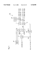
FIG. 19 is a circuit diagram illustrating a prior art multiplexer. In the figure, reference numeral 3a designates an m:1 multiplexer block (hereinafter referred to as MUX block) for converting m (m=integer, 2≦m) parallel data inputs to serial data. The m:1 multiplexer block comprises a number of D flip-flops equal to the input parallel data. Reference numeral 4 designates a D flip-flop for timing control. Reference numeral 5a designates a frequency divider that divides the frequency of an input clock signal to produce an output signal having a frequency that is an exact integral submultiple of the input frequency. The integral submultiple depends on the circuit structure of the m:1 MUX block 3a. Reference numeral 60 designates a parallel data input terminal. Reference numeral 61 designates a serial data output terminal. Reference characters S1 to Sn (n=integer, 2≦n) designate output stages. Reference character CLK designates a high-speed clock. Reference numeral 64 designates a high-speed clock input terminal.
As shown in FIG. 19, the prior art multiplexer comprises the output stages S1 to Sn, and the final output stage Sn includes the D flip-flop 4 that synchronizes the serial data output from the previous stage Sn-1 with the high-speed clock input CLK. The j-th stage Sj (j=integer, 1≦j≦n-1) includes mn-j-1 m:1 MUX blocks 3a for converting the m parallel data, which data are input to the parallel data input terminal 60 when j=1 and are input to the j-th stage Sj from the previous stage Sj-1 when j>1, into serial data using a clock signal that is obtained by dividing the clock input CLK using the (n-j) frequency dividers 5a. The mn-j-1 m:1 MUX blocks 3a in the Sj stage are connected to the next stage so that the serial data output from each m:1 MUX block 3a in the Sj stage becomes one of the parallel data input to the m:1 MUX block 3a in the next stage or becomes serial data input to the D flip-flop 4 in the Sn stage.
In the prior art multiplexer comprising the n output stages, a plurality of parallel data inputs to the input terminal 60 are successively converted into serial data by the m:1 MUX blocks 3a, and serial data is produced at the Sn-1 stage prior to the final stage. This serial data is synchronized with the clock CLK at the final stage Sn and output from the output terminal 61 as a serial data output.
FIG. 12 is a block diagram for explaining the operating principle of the prior art multiplexer. In the figure, the same reference numerals as those shown in FIG. 19 designate the same or corresponding parts. The multiplexer 200 includes 2:1 MUX blocks 1, 2, and 3 corresponding to the m:1 MUX blocks 3a, 1/2 frequency dividers 5 and 5b corresponding to the frequency dividers 5a, and a D flip-flop 4. Reference character SIG1 denotes a serial data output from the 2:1 MUX block 3.
Although the multiplexer 200 is a 4:1 multiplexer converting four bit parallel data into serial data, the operating principle is identical even when the bit number of the input parallel data is changed.
FIG. 13 is a block diagram illustrating a circuit structure of the 2:1 MUX blocks 1 to 3 shown in FIG. 12. In FIG. 13, reference numeral 7 designates a D flip-flop, numeral 8 designates a D flip-flop with a phase shifter, and numeral 9 designates a two-input selector. More specifically, the D flip-flop 7 latches the input data and outputs the data synchronously with clocks input to the 2:1 MUX block. The D flip-flop 8 with the phase shifter latches the input data, delays the phase of the data by 1/2 period of the clock input to the 2:1 MUX block, and outputs the data. The two-input selector 9 selects one of the outputs from the D flip- flops 7 and 8 synchronously with a clock signal.
Assuming that the parallel data input to the D flip-flop 7 and the D flip-flop 8 with the phase shifter are A and B, respectively, the parallel data B input to the D flip-flop 8 is phase-delayed by 1/2 period from the parallel data A input to the D flip-flop 7 when it is input to the selector 9.
In the selector 9, the parallel data A and the parallel data B are alternatingly selected at intervals equivalent to 1/2 period of the input clock. In this way, the 2:1 MUX block converts two bit parallel data into serial data. The operation of the m:1 MUX block 3a shown in FIG. 19 is fundamentally identical to the above-described operation although the number of the D flip-flops and the operating timing of the selector are different. More specifically, in the m:1 MUX block, the number of the D flip-flops is m, and one of the m D flip-flops has no phase shifter. That is, the (m-1) D flip-flops delay the phases of the input clocks by 1/m period, 2/m period, . . . , (m-1)/m period, respectively.
A description is given of the prior art multiplexer 200 shown in FIG. 12. The multiplexer 200 comprises the 2:1 MUX blocks 1 to 3, the D flip-flop 4, and the frequency dividers 5 and 5b for dividing the frequency of an input clock to 1/2. The by 2 frequency dividers 5 and 5b produce a clock 1/2 CLK having a frequency equivalent to a half of the frequency of the high-speed clock CLK and a clock 1/4 CLK having a frequency equivalent to a quarter of the high-speed clock CLK, respectively. The first stage 2:1 MUX blocks 1 and 2 convert four bit parallel data 3, 2, 1, and 0 into two bit parallel data ODD and EVEN in response to the clock 1/4 CLK. The second stage 2:1 MUX block 3 converts the two bit parallel data ODD and EVEN into serial data SIG1 in response to the clock 1/2 CLK. Finally, the D flip-flop 4 synchronizes the serial data SIG1 with the high-speed clock CLK that is directly applied from the outside of the multiplexer 200, and obtained serial data output is output from the multiplexer 200.
FIGS. 14(a)-14(k) show a timing chart of the prior art multiplexer. More specifically, FIGS. 14(a)-14(d) show the timings of the parallel data 3, 2, 1, and 0 input to the multiplexer 200, respectively, FIGS. 14(e), 14(h), and 14(j) show the timings of the clocks 1/4 CLK, 1/2 CLK, and CLK, respectively, FIGS. 14(f) and 14(g) show the timings of the parallel data ODD and EVEN, respectively, FIG. 14(i) shows the timing of the serial data SIG1, and FIG. 14(k) shows the timing of the serial data output from the multiplexer 200. In the figures, ΔTa is a delay time in the frequency divider 5, ΔTb is a delay time in the frequency divider 5b, ΔTc is a delay time in the first stage 2:1 MUX blocks 1 and 2, ΔTd is a delay time in the second stage 2:1 MUX block 3, and ΔTe is a delay time in the D flip-flop 4.
Now, a description is given of the timing of the D flip-flop 4 in the final output stage. FIGS. 18(a)-18(c) show the relationship between a clock input and a data input in the D flip-flop 4. More specifically, FIG. 18(a) shows a clock CLK input, and FIGS. 18(b) and 18(c) show data SIG1 inputs. In the figures, reference characters Tsu and Th denote a setup time and a hold time of the D flip-flop 4, respectively. Reference numeral 19 designates a data SIG1 changing point. In order to operate the D flip-flop 4 with stability, the data should not be changed between the setup time Tsu and the hold time Th of the D flip-flop 4, and the data SIG1 should not be changed between the setup time Tsu and the hold time Th when the clock CLK rises. For example, as shown in FIG. 18(b), when the data changing point 19 is not present between the setup time Tsu and the hold time Th, the D flip-flop 4 selects the data A1. However, when the data SIG1 is changed between the setup time Tsu and the hold time Th as shown in FIG. 18(c), the D flip-flop 4 becomes unstable in selecting between the data before the data changing point 19 and the data after that point. As a result, the timing of the data output from the D flip-flop 4 varies. As shown in FIGS. 14(a)-14(k), the timing of the clock CLK that is input to the D flip-flop 4 and the timing of the data SIG1 that is obtained using the clock 1/2 CLK produced by division of the clock CLK are determined by the total of the delay times ΔTa and ΔTd. However, the delay times ΔTa and ΔTd are not always as designed and significantly vary due to variations in process parameters or the temperature of the constituents of the multiplexer circuit, so that the timing of the clock CLK is sometimes deviated from the timing of the data SIG1. Especially when the operating speed is increased, the time interval where the data SIG1 is not changed is shortened, and the timing margin for the setup time Tsu and the hold time Th of the D flip-flop 4 is reduced, resulting in difficulty in normally operating the D flip-flop 4.
FIG. 20 is a block diagram illustrating a circuit structure of a prior art demultiplexer. In the figure, reference numeral 13a designates a 1:m demultiplexer block (hereinafter referred to as DEMUX block) for converting serial data into m (m=integer, 2≦m) parallel data outputs. The 1:m demultiplexer block 13a comprises a number of D flip-flops equal to the number of the parallel data outputs. Reference numeral 14 designates a D flip-flop for timing control. Reference numeral 15a designates a frequency divider that divides the frequency of an input clock to produce an output signal having a frequency that is an exact integral submultiple of the input frequency. The integral submultiple depends on the circuit structure of the 1:m DEMUX block 13a. Reference numeral 62 designates a serial data input terminal. Reference numeral 63 designates a parallel data output terminal. Reference characters S1 to Sn (n=integer, 2≦n) designate output stages. Reference character CLK designates a high-speed clock. Reference numeral 65 designates a high-speed clock input terminal.
As shown in FIG. 20, the prior art demultiplexer comprises the output stages S1 to Sn, and the first stage S1 includes the D flip-flop 14 that synchronizes the serial data that is input to the input terminal 62 with the high-speed clock CLK. The i-th stage Si (i=integer, 2≦i≦n (n=integer, 2≦n)) includes mi-2 1:m DEMUX blocks 13a for converting the serial data which is input to the i-th stage Si from the previous stage Si-1 into m (2≦m) parallel data outputs using a clock signal that is obtained by dividing the clock input CLK using the (i-1) frequency dividers 5a. The mi-2 1:m DEMUX blocks 13a of the Si stage are connected to the previous stage so that the serial data output from the previous D flip-flop 14 or one of the parallel data output from the 1:m DEMUX block 13a of the previous stage is input to the 1:m DEMUX block 13a in the Si stage as serial data.
In the prior art demultiplexer comprising the n output stages, serial data input to the input terminal 62 is synchronized with the clock signal CLK in the S1 stage and then it is output to the S2 stage. Thereafter, the data is successively converted into parallel data by the 1:m DEMUX blocks. Finally, the parallel data are output from the output terminals of the final output stage, i.e., the Sn stage, as parallel data outputs.
FIG. 15 is a block diagram for explaining the operating principle of the prior art demultiplexer. In the figure, the same reference numerals as those shown in FIG. 20 designate the same or corresponding parts. The demultiplexer 400 includes 1:2 DEMUX blocks 11, 12, and 13 corresponding to the 1:m DEMUX blocks 13a, 1/2 frequency dividers 15 and 15b corresponding to the frequency dividers 15a, and a D flip-flop 14. Reference character SIG1 denotes serial data.
Although the demultiplexer 400 is a 1:4 demultiplexer converting serial data into four bit parallel data, the operating principle is identical even when the bit number of the output parallel data is changed.
FIG. 16 is a block diagram illustrating a circuit structure of the 1:2 DEMUX blocks 11 to 13 shown in FIG. 15. In FIG. 16, the same reference numerals as those shown in FIG. 13 designate the same or corresponding parts. The 1:2 DEMUX block comprises a D flip-flop 7 to which serial data is input and a D flip-flop 8 with a phase shifter that delays the phase of the serial data by 1/2 period of the clock with respect to the D flip-flop 7. The period of the clock CLK that is input to the 1:2 DEMUX block is twice as long as the period of the serial data. Although the serial data is input to the D flip- flops 7 and 8, since the D flip-flop 8 has the phase shifter, the serial data input to the D flip-flop 8 is delayed by one period of the data from the data input to the D flip-flop 7. Since the data output from the D flip- flops 7 and 8 are synchronized alternately, the input serial data are alternately output from the D flip-flop 7 and the D flip-flop 8. In this way, the 1:2 DEMUX block converts the serial data into two bit parallel data.
The operation of the 1:m DEMUX block 13a shown in FIG. 20 is fundamentally identical to the above-described operation although the number of the D flip-flops and the operating timing are changed. More specifically, in the 1:m DEMUX block, the number of the D flip-flops is m, and one of the m D flip-flops has no phase shifter. That is, the (m-1) D flip-flops delay the phases of the input clocks by 1/m period, 2/m period, . . . , (m-1)/m period, respectively.
A description is given of the prior art demultiplexer 400 shown in FIG. 15. The demultiplexer 400 comprises the D flip-flop 14, the 1:2 DEMUX blocks 11 to 13, and the frequency dividers 15 and 15b for dividing the frequency of an input clock to by two. The frequency dividers 15 and 15b produce a clock 1/2 CLK having a frequency equivalent to 1/2 of the frequency of the high-speed clock CLK and a clock 1/4 CLK having a frequency equivalent to 1/4 of the frequency of the high-speed clock CLK, respectively. The D flip-flop 14 synchronizes the serial data input to the demultiplexer 400 with the high-speed clock CLK and outputs serial data SIG1. The serial data SIG1 is converted into two bit parallel data ODD and EVEN by the 1:2 DEMUX block 13 in the next stage. Finally, the two bit parallel data ODD and EVEN are converted into four bit parallel data 3, 2, 1, and 0 by the 1:2 DEMUX blocks 11 and 12 in the final output stage, and these parallel data are output from the demultiplexer 400.
FIGS. 17(a)-17(k) show a timing chart of the prior art demultiplexer 400. More specifically, FIGS. 17(h)-17(k) show the timings of the parallel data 3, 2, 1, and 0 output from the demultiplexer, respectively, FIGS. 17(b), 17(d), and 17(g) show the timings of the clocks CLK, 1/2 CLK, and 1/4 CLK, respectively, FIGS. 17(e) and 17(f) show the timings of the parallel data ODD and EVEN, respectively, FIG. 17(c) shows the timing of the serial data SIG1, and FIG. 17(a) shows the timing of the serial data input to the demultiplexer. In the figures, ΔTa is a delay time in the frequency divider 15, ΔTb is a delay time in the frequency divider 15b, ΔTc is a delay time in the first stage D flip-flop 14, ΔTd is a delay time in the second stage 1:2 DEMUX block 13, and ΔTe is a delay time in the 1:2 DEMUX blocks 11 and 12 at the final output stage.
Now, a description is given of the timing of the 1:2 DEMUX block 13. Assuming that the setup time and the hold time of the D flip- flops 7 and 8 in the 1:2 DEMUX block 13 are Tsu and Th, respectively, in order to operate the 1:2 DEMUX block 13 normally, the data SIG1 must not be changed, i.e., it must be stable, between the setup time Tsu and the hold time Th when the clock 1/2 CLK rises. If the data SIG1 changes between the setup time Tsu and the hold time Th, the data selected by the D flip- flops 7 and 8 becomes unstable between the data before the data changing point 19 and the data after that point, whereby the operation becomes unstable. As a result, the timing of the data output from the D flip- flops 7 and 8 varies. The timing of the clock 1/2 CLK and the data SIG1 to be input to the 1:2 DEMUX block 13 is determined by a difference between the delay time ΔTa and the delay time ΔTc. However, the delay times ΔTa and ΔTc are not always as designed and are significantly vary due to variations in process parameters and the temperature of the constituents of the demultiplexer circuit, whereby the timing of the clock 1/2 CLK sometimes deviates from the timing of the data SIG1 that is synchronized with the clock CLK. Especially when the operating speed is increased, the time interval where the data SIG1 is not changed is shortened, and the timing margin for the setup time Tsu and the hold time Th of the D flip- flops 7 and 8 is reduced, resulting in difficulty in operating the 1:2 DEMUX block 13 normally.
SUMMARY OF THE INVENTION
It is an object of the present invention to provide a multiplexer that operates normally even when the delay times of the constituents of the multiplexer vary due to variations in process parameters and temperature.
It is another object of the present invention to provide a demultiplexer that operates normally even when the delay times of the constituents of the multiplexer vary due to variations in process parameters and temperature.
Other objects and advantages of the invention will become apparent from the detailed description that follows. The detailed description and specific embodiments described are provided only for illustration since various additions and modifications within the spirit and scope of the invention will be apparent to those of skill in the art from the detailed description.
According to a first aspect of the present invention, a multiplexer comprises a plurality of stages including an n-th stage as a final output stage (n=integer, 2≦n) and a j-th stage (j=integer, 1≦j≦n-1), wherein the n-th stage includes a D flip-flop having a clock input terminal for receiving a first clock signal, a data input terminal for receiving serial data, and a data output terminal, the D flip-flop synchronizing the clock signal with the serial data; and the j-th stage includes mn-j-1 (m=integer, 2≦m) multiplexer blocks, each multiplexer block comprising a plurality of D flip-flops and having data input terminals for receiving m parallel data and a clock input terminal for receiving a second clock signal that is produced by frequency division of the first clock signal, the multiplexer block converting the parallel data into serial data in response to the second clock signal, and the multiplexer block being connected to a multiplexer block in the next stage so that the serial data output from the multiplexer block in the j-th stage is applied as one of parallel data that is input to the multiplexer block in the next stage. The multiplexer further includes a variable delay circuit connected to the data input terminal of each multiplexer block in any of the second to the n-th stages, and the variable delay circuit delays the data input by a variable delay time. Therefore, even when the delay times of the constituents of the circuit are varied due to variations in the device parameters or the temperature and the timing of the data input is deviated, the timing of the data input is adjusted by the variable delay circuit, whereby the D flip-flop in the stage having the variable delay circuit is normally operated.
According to a second aspect of the present invention, a multiplexer comprises a plurality of stages including an n-th stage as a final output stage (n=integer, 2≦n) and a j-th stage (j=integer, 1≦j≦n-1), wherein the n-th stage includes a D flip-flop having a clock input terminal for receiving a first clock signal, a data input terminal for receiving serial data, and a data output terminal, the D flip-flop synchronizing the clock signal with the serial data; and the j-th stage includes mn-j-1 (m=integer, 2≦m) multiplexer blocks, each multiplexer block comprising a plurality of D flip-flops and having data input terminals for receiving m parallel data and a clock input terminal for receiving a second clock signal that is produced by frequency division of the first clock signal, the multiplexer block converting the parallel data into serial data in response to the second clock signal, and the multiplexer block being connected to a multiplexer block in the next stage so that the serial data output from the multiplexer block in the j-th stage is applied as one of parallel data that is input to the multiplexer block in the next stage. The multiplexer further includes a variable delay circuit connected to the clock input terminal of each multiplexer block in any of the first to the (n-1)th stages or to the clock input terminal of the D flip-flop in the n-th stage, and the variable delay circuit delays the clock input by a variable delay time. Therefore, even when the delay times of the constituents of the circuit are varied due to variations in the device parameters or the temperature and the timing of the clock input is deviated, the timing of the clock input is adjusted by the variable delay circuit, whereby the D flip-flop in the stage having the variable delay circuit is normally operated.
According to a third aspect of the present invention, a multiplexer comprises a plurality of stages including an n-th stage as a final stage (n=integer, 2≦n) and an h-th stage (h=integer, 1≦h≦n-1), wherein the n-th stage includes a multiplexer block comprising a plurality of D flip-flops and having a clock input terminal for receiving a first clock signal, a data input terminal for receiving m (m=integer, 2≦m) parallel data, and a data output terminal, the multiplexer block converting the parallel data into serial data in response to the first clock signal; and the h-th stage includes mn-h multiplexer blocks, each multiplexer block comprising a plurality of D flip-flops and having data input terminals for receiving m parallel data and a clock input terminal for receiving a second clock signal that is produced by frequency division of the first clock signal, the multiplexer block converting the parallel data into serial data in response to the second clock signal, and the multiplexer block being connected to a multiplexer block in the next stage so that the serial data output from the multiplexer block in the h-th stage is applied as one of parallel data that is input to the multiplexer block in the next stage. The multiplexer further includes a variable delay circuit connected to the data input terminal of each multiplexer block in any of the second to the n-th stages, and the variable delay circuit delays the data input by a variable delay time. Therefore, even when the delay times of the constituents of the circuit are varied due to variations in the device parameters or the temperature and the timing of the data input is deviated, the timing of the data input is adjusted by the variable delay circuit, whereby the D flip-flop in the stage having the variable delay circuit is normally operated.
According to a fourth aspect of the present invention, a multiplexer comprises a plurality of stages including an n-th stage as a final stage (n=integer, 2≦n) and an h-th stage (h=integer, 1≦h≦n-1), wherein the n-th stage includes a multiplexer block comprising a plurality of D flip-flops and having a clock input terminal for receiving a first clock signal, a data input terminal for receiving m (m=integer, 2≦m) parallel data, and a data output terminal, the multiplexer block converting the parallel data into serial data in response to the first clock signal; and the h-th stage includes mn-h multiplexer blocks, each multiplexer block comprising a plurality of D flip-flops and having data input terminals for receiving m parallel data and a clock input terminal for receiving a second clock signal that is produced by frequency division of the first clock signal, the multiplexer block converting the parallel data into serial data in response to the second clock signal, and the multiplexer block being connected to a multiplexer block in the next stage so that the serial data output from the multiplexer block in the h-th stage is applied as one of parallel data that is input to the multiplexer block in the next stage. The multiplexer further includes a variable delay circuit connected to the clock input terminal of each multiplexer block in any of the first to the (n-1)th stages or to the clock input terminal of the multiplexer block in the n-th stage, and the variable delay circuit delays the clock input by a variable delay time. Therefore, even when the delay times of the constituents of the circuit are varied due to variations in the device parameters or the temperature and the timing of the clock input is deviated, the timing of the clock input is adjusted by the variable delay circuit, whereby the D flip-flop in the stage having the variable delay circuit is normally operated.
According to a fifth aspect of the present invention, the above-described multiplexers further include means for monitoring data output from the data output terminal of the D flip-flop or the multiplexer block in the final n-th stage; and means for controlling the delay time of the variable delay circuit with a control signal according to the result of the monitoring. Therefore, even when the delay times of the constituents of the circuit are varied due to variations in the device parameters or the temperature and the timing of the data input or the clock input is deviated, the deviation of the timing is monitored and the delay time of the variable delay circuit is controlled according to the result of the monitoring so that the deviation of the timing is prevented, thereby providing a normally operating multiplexer.
According to a sixth aspect of the present invention, in the above-described multiplexers, the variable delay circuit comprises a plurality of lines comprising buffers in different numbers and providing different delay times, the lines being arranged in parallel with each other; and a selector for selecting one of the lines in response to the control signal supplied from the delay time controlling means, the selector being connected to the lines and the delay time controlling means. Therefore, the delay time of the variable delay circuit is easily controlled by switching the lines using the selector, thereby providing a multiplexer that is easily adjusted to the normal operating state even when the delay times of the constituents of the circuit are varied.
According to a seventh aspect of the present invention, in the above-described multiplexers, the variable delay circuit comprises at least a variable delay buffer that is connected to the delay time controlling means and varies the delay time in response to the control signal supplied from the delay time controlling means. Therefore, the delay time of the variable delay circuit is easily controlled by varying the delay time of the variable delay buffer with the control signal, thereby providing a multiplexer that is easily adjusted to the normal operating state even when the delay times of the constituents of the circuit are varied.
According to an eighth aspect of the present invention, in the above-described multiplexers, the variable delay buffer comprises a source follower buffer including a current supply transistor, and the delay time is controlled by controlling a gate voltage of the current supply transistor with the control signal supplied from the delay time controlling means.
According to a ninth aspect of the present invention, a demultiplexer comprises a plurality of stages including a first stage and an i-th stage (i=integer, 2≦i≦n (n=integer, 2≦n)), wherein the first stage includes a D flip-flop having a clock input terminal for receiving a first clock signal, a data input terminal for receiving serial data, and a data output terminal, the D flip-flop synchronizing the clock signal with the serial data; and the i-th stage including mi-2 (m=integer, 2≦m) demultiplexer blocks, each demultiplexer block comprising a plurality of D flip-flops and having a data input terminal for receiving serial data and a clock input terminal for receiving a second clock signal that is produced by frequency division of the first clock signal, the demultiplexer block converting the serial data into m parallel data in response to the second clock signal, and the demultiplexer block being connected to a demultiplexer block in the prior stage so that one of parallel data output from the demultiplexer block in the prior stage is input to each demultiplexer block in the i-th stage as the serial data input. The demultiplexer further includes a variable delay circuit connected to the data input terminal of each demultiplexer block in any of the second to the n-th stages, and the variable delay circuit delays the data input by a variable delay time. Therefore, even when the delay times of the constituents of the circuit are varied due to variations in the device parameters or the temperature and the timing of the data input is deviated, the timing of the data input is adjusted by the variable delay circuit, whereby the D flip-flop in the stage having the variable delay circuit is normally operated.
According to a tenth aspect of the present invention, a demultiplexer comprises a plurality of stages including a first stage and an i-th stage (i=integer, 2≦i≦n (n=integer, 2≦n)), wherein the first stage includes a D flip-flop having a clock input terminal for receiving a first clock signal, a data input terminal for receiving serial data, and a data output terminal, the D flip-flop synchronizing the clock signal with the serial data; and the i-th stage includes mi-2 (m=integer, 2≦m) demultiplexer blocks, each demultiplexer block comprising a plurality of D flip-flops and having a data input terminal for receiving serial data and a clock input terminal for receiving a second clock signal that is produced by frequency division of the first clock signal, the demultiplexer block converting the serial data into m parallel data in response to the second clock signal, and the demultiplexer block being connected to a demultiplexer block in the prior stage so that one of parallel data output from the demultiplexer block in the prior stage is input to each demultiplexer block in the i-th stage as the serial data input. The demultiplexer further includes a variable delay circuit connected to the clock input terminal of each demultiplexer block in any of the second to the n-th stages or to the clock input terminal of the D flip-flop in the first stage, and the variable delay circuit delays the clock input by a variable delay time. Therefore, even when the delay times of the constituents of the circuit are varied due to variations in the device parameters or the temperature and the timing of the clock input is deviated, the timing of the clock input is adjusted by the variable delay circuit, whereby the D flip-flop in the stage having the variable delay circuit is normally operated.
According to an eleventh aspect of the present invention, a demultiplexer comprises a plurality of stages including a first stage and a k-th stage (k=integer, 2≦k≦n (n=integer, 2≦n)), wherein the first stage includes a demultiplexer block comprising a plurality of D flip-flops and having a clock input terminal for receiving a first clock signal, a data input terminal for receiving serial data, and a data output terminal, the demultiplexer block converting the serial data into m (m=integer, 2≦m) parallel data in response to the first clock signal; and the k-th stage includes mk-1 demultiplexer blocks, each demultiplexer block comprising a plurality of D flip-flops and having a data input terminal for receiving serial data and a clock input terminal for receiving a second clock signal that is produced by frequency division of the first clock signal, the demultiplexer block converting the serial data into m parallel data in response to the second clock signal, and the demultiplexer block being connected to a demultiplexer block in the prior stage so that one of parallel data output from the demultiplexer block in the prior stage is input to each demultiplexer block in the k-th stage as the serial data input. The demultiplexer further includes a variable delay circuit connected to the data input terminal of each demultiplexer block in any of the second to the n-th stages, and the variable delay circuit delays the data input by a variable delay time. Therefore, even when the delay times of the constituents of the circuit are varied due to variations in the device parameters or the temperature and the timing of the data input is deviated, the timing of the data input is adjusted by the variable delay circuit, whereby the D flip-flop in the stage having the variable delay circuit is normally operated.
According to a twelfth aspect of the present invention, a demultiplexer comprises a plurality of stages including a first stage and a k-th stage (k=integer, 2≦k≦n (n=integer, 2≦n)), wherein the first stage includes a demultiplexer block comprising a plurality of D flip-flops and having a clock input terminal for receiving a first clock signal, a data input terminal for receiving serial data, and a data output terminal, the demultiplexer block converting the serial data into m (m=integer, 2≦m) parallel data in response to the first clock signal; and the k-th stage includes mk-1 demultiplexer blocks, each demultiplexer block comprising a plurality of D flip-flops and having a data input terminal for receiving serial data and a clock input terminal for receiving a second clock signal that is produced by frequency division of the first clock signal, the demultiplexer block converting the serial data into m parallel data in response to the second clock signal, and the demultiplexer block being connected to a demultiplexer block in the prior stage so that one of parallel data output from the demultiplexer block in the prior stage is input to each demultiplexer block in the k-th stage as the serial data input. The demultiplexer further includes a variable delay circuit connected to the clock input terminal of each demultiplexer block in any of the second to the n-th stages or to the clock input terminal of the D flip-flop in the first stage, and the variable delay circuit delays the clock input by a variable delay time. Therefore, even when the delay times of the constituents of the circuit are varied due to variations in the device parameters or the temperature and the timing of the clock input is deviated, the timing of the clock input is adjusted by the variable delay circuit, whereby the D flip-flop in the stage having the variable delay circuit is normally operated.
According to a thirteenth aspect of the present invention, the above-described demultiplexers further include means for monitoring data output from the data output terminals of the demultiplexer blocks in the final n-th stage; and means for controlling the delay time of the variable delay circuit with a control signal according to the result of the monitoring. Therefore, even when the delay times of the constituents of the circuit are varied due to variations in the device parameters or the temperature and the timing of the data input or the clock input is deviated, the deviation of the timing is monitored and the delay time of the variable delay circuit is controlled according to the result of the monitoring so that the deviation of the timing is prevented, thereby providing a normally operating demultiplexer.
According to a fourteenth aspect of the present invention, in the above-described demultiplexers, the variable delay circuit comprises a plurality of lines comprising buffers in different numbers and providing different delay times, the lines being arranged in parallel with each other; and a selector for selecting one of the lines in response to the control signal supplied from the delay time controlling means, the selector being connected to the lines and the delay time controlling means. Therefore, the delay time of the variable delay circuit is easily controlled by switching the lines using the selector, thereby providing a demultiplexer that is easily adjusted to the normal operating state even when the delay times of the constituents of the circuit are varied.
According to a fifteenth aspect of the present invention, in the above-described demultiplexers, the variable delay circuit comprises at least a variable delay buffer that is connected to the delay time controlling means and varies the delay time in response to the control signal supplied from the delay time controlling means. Therefore, the delay time of the variable delay circuit is easily controlled by varying the delay time of the variable delay buffer with the control signal, thereby providing a demultiplexer that is easily adjusted to the normal operating state even when the delay times of the constituents of the circuit are varied.
According to a sixteenth aspect of the present invention, in the above-described demultiplexers, the variable delay buffer comprises a source follower buffer including a current supply transistor, and the delay time is controlled by controlling a gate voltage of the current supply transistor with the control signal supplied from the delay time controlling means.
BRIEF DESCRIPTION OF THE DRAWINGS
FIG. 1 is a block diagram illustrating a circuit structure of a multiplexer in accordance with a first embodiment of the present invention.
FIGS. 2(a)-2(l) are diagrams illustrating a timing chart of the multiplexer according to the first embodiment of the invention.
FIG. 3 is a block diagram illustrating a circuit structure of a multiplexer in accordance with a second embodiment of the present invention.
FIG. 4 is a block diagram illustrating a circuit structure of a demultiplexer in accordance with a fourth embodiment of the present invention.
FIGS. 5(a)-5(l) are diagrams illustrating a timing chart of the demultiplexer according to the fourth embodiment of the present invention.
FIG. 6 is a block diagram illustrating a circuit structure of a demultiplexer in accordance with a fifth embodiment of the present invention.
FIG. 7 is a block diagram illustrating a variable delay circuit included in a multiplexer according to the first embodiment of the invention.
FIG. 8 is a block diagram illustrating a variable delay circuit included in the multiplexer in accordance with a seventh embodiment of the invention.
FIG. 9 is a block diagram illustrating a circuit structure of a variable delay buffer included in the variable delay circuit according to the seventh embodiment of the invention.
FIG. 10 is a block diagram illustrating a circuit structure of a multiplexer in accordance with a third embodiment of the present invention.
FIG. 11 is a block diagram illustrating a circuit structure of a demultiplexer in accordance with a sixth embodiment of the present invention.
FIG. 12 is a block diagram illustrating a circuit structure of a 4:1 multiplexer according to the prior art.
FIG. 13 is a block diagram illustrating a circuit structure of a 2:1 multiplexer block included in the prior art multiplexer.
FIGS. 14(a)-14(k) are diagrams illustrating a timing chart of the prior art multiplexer.
FIG. 15 is a block diagram illustrating a circuit structure of a 1:4 demultiplexer according to the prior art.
FIG. 16 is a block diagram illustrating a circuit structure of a 1:2 demultiplexer block included in the prior art demultiplexer.
FIGS. 17(a)-17(k) are diagrams illustrating a timing chart of the prior art demultiplexer.
FIGS. 18(a)-18(c) are diagrams illustrating a timing chart of a clock input and a data input in a D flip-flop of the prior art multiplexer.
FIG. 19 is a block diagram illustrating a circuit structure of the prior art multiplexer.
FIG. 20 is a block diagram illustrating a circuit structure of the prior art demultiplexer.
DETAILED DESCRIPTION OF THE PREFERRED EMBODIMENTS
Embodiment 1!
FIG. 1 is a block diagram illustrating a circuit structure of a multiplexer in accordance with a first embodiment of the present invention. In the figure, the same reference numerals as those in FIG. 12 designate the same or corresponding parts. Reference numeral 100 designates a multiplexer according to this first embodiment of the invention. The multiplexer 100 comprises 2:1 MUX blocks 1, 2, and 3, a variable delay circuit 10, a D flip- flop 4, 1/2 frequency dividers 5 and 5b, a monitor 20, and a control circuit 30. More specifically, the 2:1 MUX block 1 receives parallel data 3 and 1 and outputs parallel data ODD. The 2:1 MUX block 2 receives parallel data 2 and 0 and outputs parallel data EVEN. The 2:1 MUX block 3 receives the parallel data ODD and EVEN output from the 2:1 MUX blocks 1 and 2, respectively, and outputs serial data SIG1. The variable delay circuit 10 receives the serial data SIG1 output from the 2:1 MUX block 3, delays the serial data SIG1 by a variable delay time, and outputs serial data SIG2.
Further, the control circuit 30 is connected to the variable delay circuit 10 and controls the variable delay circuit 10 with a control signal that determines the delay time. The D flip-flop 4 receives the serial data SIG2 output from the variable delay circuit 10. The monitor 20 is connected to an output terminal of the D flip-flop 4. The monitor 20 monitors the serial data output from the D flip-flop 4 and compares the serial data with an expected value that is input to the monitor 20 in advance. For example, a measuring instrument or a combination of a measuring instrument and a computer is employed as the monitor 20. A high-speed clock CLK supplied from outside of the multiplexer is input to the D flip-flop 4 and to the 1/2 frequency divider 5. The 1/2 frequency divider 5 divides the frequency of the high-speed clock CLK and produces a clock 1/2 CLK. The clock 1/2 CLK is input to the 2:1 MUX block 3 and to the 1/2 frequency divider 5b. The 1/2 frequency divider 5b divides the frequency of the clock 1/2 CLK and produces a clock 1/4 CLK. The clock 1/4 CLK is input to the 2:1 MUX blocks 1 and 2.
The multiplexer according to the first embodiment of the invention is fundamentally identical to the prior art multiplexer shown in FIG. 19 in which the final output stage Sn includes the D flip-flop 4 that synchronizes the clock input CLK with the serial data supplied from the previous stage Sn-1, and the j-th stage Sj (j=integer, 1≦j≦n-1) includes mn-j-1 m:1 MUX blocks 3a for converting the m parallel data into serial data using a clock signal that is obtained by dividing the clock input CLK using the (n-j) frequency dividers 5a. However, the multiplexer according to the first embodiment further includes a monitor for monitoring an output from the D flip-flop 4 in the final output stage, a variable delay circuit connected to the data input terminal of the D flip-flop 4, and a control circuit for controlling the variable delay circuit, whereby the variable delay circuit is controlled by the control circuit according to the result of the monitoring to adjust the variable delay time.
Although the multiplexer 100 according to the first embodiment of the invention is a 4:1 multiplexer, the monitor 20, the variable delay circuit 10, and the control circuit 30 may be applied to a multiplexer including n stages of m:1 MUX blocks as shown in FIG. 19 with the same operating principle and the same effects.
FIG. 7 is a block diagram illustrating a structure of the variable delay circuit 10 according to this first embodiment of the invention. In the figure, reference numeral 23 designates an input terminal of the variable delay circuit 10 to which the serial data SIG1 is applied. Reference numeral 22 designates a 2r :1 selector that has 2r data input terminals and selects one of 2r data inputs. One of the 2r input terminals of the selector 22 is connected to the input terminal 23 of the variable delay circuit 10. The selector 22 is controlled by control signals L1 to Lr which are input to control signal input terminals 24. The data SIG2 selected in the selector 22 is output from the data output terminal 25. A plurality of lines 210 in which one, two, four, . . . , and 2r-1 buffers 21 are respectively connected in series (hereinafter referred to as buffer lines) are connected between the input terminal 23 and the (2r -1) input terminals of the selector 22.
In this first embodiment of the invention, in order to vary the delay time of the variable delay circuit 10, the delay times of the respective buffer lines 210 are varied by changing the number of the buffers 21 included in the buffer lines 210. Alternatively, the delay times of the respective buffer lines 210 can be varied by changing the kind, fan-out number, fan-in number, wiring length, or I/O method of the buffers included in the respective buffer lines.
FIGS. 2(a)-2(l) are diagrams illustrating a timing chart of the multiplexer 100 according to this first embodiment of the invention. More specifically, FIGS. 2(a)-2(d) show the timings of the parallel data 3, 2, 1, and 0 input to the multiplexer 100, respectively, FIGS. 2(e) and 2(h) show the timings of the clocks 1/4 CLK and 1/2 CLK, respectively, FIGS. 2(f) and 2(g) show the timings of the parallel data ODD and EVEN, respectively, FIG. 2(i) shows the timing of the serial data SIG1, FIG. 2(k) shows the timing of the high-speed clock CLK, FIG. 2(j) shows the timing of the serial data SIG2 output from the variable delay circuit 10, and FIG. 2(l) shows the timing of the serial data output from the D flip-flop 4. In these figures, the same reference characters as those shown in FIGS. 14(a)-14(k) denote the same or corresponding elements. Reference character ΔT denotes a delay time in the variable delay circuit 10.
First of all, the operation of the variable delay circuit 10 shown in FIG. 7 will be described. The input terminal 23 to which the data SIG1 is input is connected to the selector 22 through the buffer lines 210 which are arranged in parallel and include the buffers 21 in different numbers. The selector 22 selects one of the buffer lines 210 in response to a control signal that is supplied from the control circuit 30 through the control signal input terminal 24 to the selector 22. Thereby, the number of the buffers 21 through which the input data SIG1 travels is changed, and a desired delay time is obtained. For example, when the variable delay circuit has r (r=integer) control signal input terminals 24 to which control signals L1 to Lr are applied, one of 2r buffer lines respectively including different numbers of buffers is selected, whereby 2r stages of delay are possible. In this way, a line having an optimum delay time is selected from a plurality of lines with different delay times using control signals L1 -Lr, whereby the delay time of the data output SIG2 is easily varied.
A description is given of the operation of the multiplexer according to the first embodiment of the invention. initially, a high-speed clock CLK is divided using the frequency dividers 5 and 5b to produce a clock 1/2 CLK having a frequency equivalent to 1/2 of the frequency of the high-speed clock CLK and a clock 1/4 CLK having a frequency equivalent to 1/4 of the frequency of the high-speed clock CLK. In the first stage 2:1 MUX blocks 1 and 2, using the clock 1/4 CLK, four bit parallel data 3, 2, 1, and 0 are converted into two bit parallel data ODD and EVEN. In the second stage 2:1 MUX block 3, using the clock 1/2 CLK, the two bit parallel data ODD and EVEN are converted into serial data SIG1. Then, this serial data SIG1 is delayed by ΔT by the variable delay circuit 10 to produce serial data SIG2. Finally, by the D flip-flop 4 at the final output stage, the serial data SIG2 is synchronized with the high-speed clock CLK that is directly input from the outside of the multiplexer 100, whereby the serial data SIG2 is delayed by ΔTe. The serial data output obtained from the D flip-flop 4 is output from the multiplexer 100.
In the multiplexer 100 according to the first embodiment of the invention, known parallel data 3, 2, 1, 0 for testing are input to a multiplexer identical to the multiplexer 100 and kept at a temperature proximate to an actual operating temperature, and an output from the final output stage is monitored using the monitor 20. The delay time ΔT of the data SIG2 in the variable delay circuit 10 is adjusted in response to a control signal supplied from the control circuit 30 so that the monitored value becomes equivalent to an expected value for the serial data output obtained from the parallel data for test. In the prior art multiplexer 200, the delay times of the constituents of the circuit are unfavorably varied due to variations in the process parameters and the temperature, so that the timing of the high-speed clock CLK and the serial data SIG1 to be input to the D flip-flop 4 vary from the design timing, whereby the D flip-flop 4 is not normally operated.
However, in this first embodiment of the invention, the delay time of the variable delay circuit 10 is adjusted in advance. Therefore, even when the timing of the high-speed clock CLK and the serial data SIG1 varies from the design timing and the data changing point of the serial data SIG1 is placed between the setup time and the hold time of the D flip-flop 4, since the timing of the serial data SIG1 is adjusted in the variable delay circuit 10 and the timing-adjusted serial data SIG2 is input to the D flip-flop 4, the data changing point of the data input SIG2 is prevented from being placed between the setup time and the hold time of the D flip-flop 4, whereby the deviation of the timing in the final output stage, i.e., the D flip-flop 4, is avoided. As a result, the multiplexer 100 is normally operated.
The control of the output signal from the control circuit according to the result of the monitoring may be manually performed. Alternatively, the control of the output signal may be automated with the result of the monitoring in advance.
As described above, in the multiplexer according to the first embodiment of the invention, the variable delay circuit 10 is connected to the data input terminal of the D flip-flop 4 for timing control, and the delay time of the variable delay circuit 10 is controlled by the control circuit in response to the output of the D flip-flop 4 that is monitored by the monitor 20, whereby the timing of the serial data input to the D flip-flop is adjusted. Therefore, even when the delay times of the constituents of the circuit vary due to variations in device parameters and temperature, it is possible to normally operate the D flip-flop 4 using the timing-adjusted serial data, whereby the multiplexer operates normally.
Furthermore, in this first embodiment of the invention, since the variable delay circuit 10 includes the selector 22 that selects one of the buffer lines 210 comprising different numbers of the buffers 21 and having different delay times, the delay time of the variable delay circuit 10 is easily varied by switching the buffer lines 210 of the selector 22, whereby a normally operating multiplexer is provided even when the delay times of the constituents of the circuit are varied.
In this first embodiment of the invention, the variable delay circuit 10 is connected to the data input terminal of the D flip-flop 4 in the final output stage. However, a similar structure in which the variable delay circuit is connected to the data input terminals of the MUX blocks constituting any of the other output stages, except the first output stage, is also within the scope of the invention. In this case, the variable delay circuit must be connected to the data input terminals of all of the D flip-flops constituting the output stage.
Embodiment 2!
FIG. 3 is a block diagram illustrating a circuit structure of a multiplexer in accordance with a second embodiment of the present invention. In the figure, the same reference numerals as those in FIG. 1 designate the same or corresponding parts. Reference numeral 101 designates a multiplexer according to this second embodiment of the invention. The multiplexer 101 comprises 2:1 MUX blocks 1, 2, and 3, a variable delay circuit 10, a D flip- flop 4, 1/2 frequency dividers 5 and 5b, a monitor 20, and a control circuit 30. More specifically, the 2:1 MUX block 1 receives parallel data 3 and 1 and outputs parallel data ODD. The 2:1 MUX block 2 receives parallel data 2 and 0 and outputs parallel data EVEN. The 2:1 MUX block 3 receives the parallel data ODD and EVEN output from the 2:1 MUX blocks 1 and 2, respectively, and outputs serial data SIG1. The D flip-flop 4 receives the serial data SIG1 output from the 2:1 MUX block 3. The monitor 20 is connected to an output terminal of the D flip-flop 4. The monitor 20 monitors the serial data output from the D flip-flop 4 and compares the serial data with an expected value that is input to the monitor 20 in advance. For example, a measuring instrument or a combination of a measuring instrument and a computer is employed as the monitor 20. Further, the variable delay circuit 10 receives a high-speed clock CLK supplied from outside of the multiplexer and delays the high-speed clock CLK. The variable delay circuit 10 controls the delay time of the input signal at variable values. The control circuit 30 is connected to the variable delay circuit 10 and controls the variable delay circuit 10 with a control signal that determines the delay time. The 1/2 frequency divider 5 divides the frequency of the high-speed clock CLK and produces a clock 1/2 CLK. The clock 1/2 CLK is input to the 2:1 MUX block 3 and the 1/2 frequency divider 5b. The 1/2 frequency divider 5b divides the frequency of the clock 1/2 CLK and produces a clock 1/4 CLK. The clock 1/4 CLK is input to the 2:1 MUX blocks 1 and 2.
While in the first embodiment of the invention the variable delay circuit 10 is connected to the data input terminal of the D flip-flop 4 in the final output stage, in this second embodiment it is connected to the clock input terminal of the D flip-flop 4, whereby the clock signal input to the D flip-flop 4 is delayed at variable values.
In this second embodiment of the invention, the variable delay circuit 10 is connected to the clock input terminal of the D flip-flop 4 in the final output stage. However, a similar structure in which the variable delay circuit is connected to the frequency-divided clock input terminals of the MUX blocks constituting any of other output stages is also within the scope of the invention. In this case, the variable delay circuit must be connected to the frequency-divided clock input terminals of all of the D flip-flops constituting the output stage.
The operation of the 4:1 multiplexer according to the second embodiment of the invention will be described.
In the first embodiment of the invention, when the timing of the high-speed clock CLK and the data input SIG1 to be input to the D flip-flop 4 vary from the design timing, a control signal supplied from the control circuit 30 is input to the variable delay circuit 10 to adjust the timing of the data input SIG1 and produce a data input SIG2, and the data input SIG2 is input to the D flip-flop 4, whereby the D flip-flop 4 is normally operated. On the other hand, in this second embodiment, when the timing of the high-speed clock CLK and the data input SIG1 to be input to the D flip-flop 4 vary from the design timing, a clock adjusted by delaying the high-speed clock CLK by the variable delay circuit 10 is input to the D flip-flop 4, whereby the timing of the high-speed clock CLK and the data input SIG1 is made proximate to the design timing.
Initially, the high-speed clock CLK is divided by the frequency dividers 5 and 5b to produce a clock 1/2 CLK having a frequency equivalent to 1/2 of the frequency of the high-speed clock CLK and a clock 1/4 CLK having a frequency equivalent to 1/4 of the frequency of the high-speed clock CLK. In the first stage 2:1 MUX blocks 1 and 2, using the clock 1/4 CLK, four bit parallel data 3, 2, 1, and 0 are converted into two bit parallel data ODD and EVEN. In the second stage 2:1 MUX block 3, using the clock 1/2 CLK, the two bit parallel data ODD and EVEN are converted into serial data SIG1. Then, this serial data SIG1 is input to the D flip-flop 4 in the final output stage. Since a clock signal that is obtained by delaying the high-speed clock CLK by ΔT by the variable delay circuit 10 is input to the D flip-flop 4, the input serial data SIG1 is synchronized with the delayed high-speed clock and delayed by ΔTe. Finally, thus obtained serial data is output from the multiplexer 101.
In the multiplexer 101 according to the second embodiment of the invention, known parallel data 3, 2, 1, 0 for test are input to a multiplexer identical to the multiplexer 101 according to the second embodiment and kept at a temperature proximate to an actual operating temperature, and an output from the final output stage is monitored using the monitor 20. The delay time ΔT of the high-speed clock CLK in the variable delay circuit 10 is adjusted in response to a control signal supplied from the control circuit 30 so that the monitored value becomes the same as an expected value for the serial data output obtained from the parallel data for test. In the prior art multiplexer 200, the delay times of the constituents of the circuit are unfavorably varied due to variations in the process parameters and the temperature, so that the timing of the high-speed clock CLK and the data input SIG1 to be input to the D flip-flop 4 varies from the design timing, whereby the D flip-flop 4 is not normally operated.
However, in this second embodiment of the invention, the delay time of the variable delay circuit 10 is adjusted in advance. Therefore, even when the timing of the high-speed clock CLK and the data input SIG1 to be input to the D flip-flop 4 varies from the design timing and the data changing point of the data input SIG1 is located between the setup time and the hold time of the D flip-flop 4, since the deviation of the timing is adjusted by delaying the high-speed clock CLK in the variable delay circuit 10, the changing point of the output from the D flip-flop 4 is prevented from being placed between the setup time and the hold time of the D flip-flop 4. As a result, the deviation of the timing in the final output stage, i.e., the D flip-flop 4, is avoided, whereby the multiplexer 101 is normally operated.
The control of the output signal using the control circuit according to the result of the monitoring may be manually performed. Alternatively, the control of the output signal may be automated with the result of the monitoring in advance.
As described above, in the multiplexer according to the second embodiment of the invention, the variable delay circuit 10 is connected to the clock input terminal of the D flip-flop 4 in the final output stage, and the delay time of the variable delay circuit 10 is controlled to adjust the timing of the clock input to the D flip-flop 4. Therefore, even when the delay times of the constituents of the circuit to vary due to variations in the device parameters and the temperature and the timing of the data input varies from the timing of the clock input or the divided clock input, since the delay time of the variable delay circuit is adjusted by the control circuit according to the result of the monitoring so that the deviation is prevented, the D flip-flop provided with the variable delay circuit is normally operated.
Furthermore, since the variable delay circuit 10 includes the selector 22 that selects one of the buffer lines 210 comprising the buffers 21 and having different delay times, the delay time of the variable delay circuit 10 is easily varied by switching the buffer lines 210 in the selector 22. Therefore, a normally operating multiplexer is realized even when the delay times of the constituents of the circuit are varied.
Embodiment 3!
FIG. 10 is a block diagram illustrating a circuit structure of a multiplexer in accordance with a third embodiment of the present invention. In the figure, the same reference numerals as those shown in FIG. 1 designate the same or corresponding parts. Reference numeral 102 designates a multiplexer according to the third embodiment of the invention. The multiplexer 102 comprises 2:1 MUX blocks 1, 2, and 3, variable delay circuits 10a and 10b, a 1/2 frequency divider 5b, a monitor 20, and a control circuit 30. More specifically, the 2:1 MUX block 1 receives parallel data inputs 3 and 1 and outputs serial data. The 2:1 MUX block 2 receives parallel data inputs 2 and 0 and outputs serial data. The variable delay circuits 10a and 10b receive the serial data output from the 2:1 MUX blocks 1 and 2 and delay the serial data, respectively. These variable delay circuits 10a and 10b are identical to the variable delay circuit 10 according to the first and second embodiments.
Further, the control circuit 30 is connected to the variable delay circuits 10a and 10b and controls the variable delay circuits 10a and 10b with a control signal that determines the delay time. The variable delay circuits 10a and 10b output data ODD and data EVEN, respectively, and these data ODD and EVEN are input to the 2:1 MUX block 3. The monitor 20 is connected to an output terminal of the 2:1 MUX block 3. The monitor 20 monitors the serial data output from the 2:1 MUX block 3 and compares the serial data with an expected value that is input to the monitor 20 in advance. For example, a measuring instrument or a combination of a measuring instrument and a computer is employed as the monitor 20. The 1/2 frequency divider 5 divides the frequency of the high-speed clock CLK supplied from the outside of multiplexer and produces a clock 1/2 CLK. The clock 1/2 CLK is input to the 2:1 MUX blocks 1 and 2.
In the first embodiment of the invention, a variable delay circuit is included in a multiplexer in which serial data is synchronized with a clock input in a D flip-flop at the final output stage. In this third embodiment, however, the final output stage, i.e., the n-th stage (n=integer, 2≦n), includes an m:1 MUX block that converts m (m=integer, 2≦m) parallel data into serial data using a clock signal. The h-th stage (h 32 integer, 1≦h≦n-1) includes mn-h m:1 MUX blocks that convert the m parallel data into serial data using a frequency-divided clock input obtained by frequency division of the clock signal. In this structure, variable delay circuits are connected to the data input terminals of the m:1 MUX block in the final output stage, i.e., the n-th stage.
In this third embodiment, the variable delay circuits 10a and 10b are connected to the data input terminals of the MUX block 3 in the final output stage. However, a similar structure in which the variable delay circuits are connected to the clock input terminals or the frequency-divided clock input terminals of the MUX blocks constituting any output stage is also within the scope of the invention. In this case, the variable delay circuit must be connected to the clock input terminals or the frequency-divided clock input terminals of all of the D flip-flops constituting the output stage. Likewise, a similar structure in which the variable delay circuits are connected to the data input terminals of the MUX blocks constituting any other output stages, except the first output stage, is also within the scope of the invention. In this case, the variable delay circuits must be connected to the data input terminals of all of the D flip-flops constituting the output stage.
A description is given of the operation of the 4:1 multiplexer according to the third embodiment of the invention. While in the first embodiment of the invention the variable delay circuit 10 is included in a multiplexer in which the serial data SIG1 are synchronized with the clock CLK by the D flip-flop 4 in the final output stage, in this third embodiment of the invention the final output stage is constituted by the 2:1 MUX block 3 and the variable delay circuits 10a and 10b are connected to the data input terminals of the 2:1 MUX block 3 in the final output stage.
Initially, the high-speed clock CLK is divided by the frequency divider 5b to produce a clock 1/2 CLK having a frequency equivalent to 1/2 of the frequency of the high-speed clock CLK. In the first stage 2:1 MUX blocks 1 and 2, using the clock 1/2 CLK, four bit parallel data 3, 2, 1, and 0 are converted into two bit parallel data. These two bit parallel data are delayed in the variable delay circuits 10a and 10b, respectively, producing two bit parallel data ODD and EVEN. These parallel data ODD and EVEN are converted into serial data by the 2:1 MUX block 3 and this serial data is output from the multiplexer 102.
In the multiplexer 102 according to the third embodiment of the invention, known parallel data inputs 3, 2, 1, and 0 for test are input to a multiplexer identical to the multiplexer 102 according to the third embodiment and kept at a temperature proximate to an actual operating temperature, and an output from the final output stage is monitored using the monitor 20. The delay times of the output data from the 2:1 MUX blocks 1 and 2 in the variable delay circuits 10a and 10b are controlled in response to a control signal output from the control circuit 30 so that the monitored value becomes equivalent to an expected value for the serial data output obtained from the parallel data for test. In the prior art multiplexer 200, the delay times of the constituents of the circuit are unfavorably varied due to variations in the process parameters and the temperature, so that the timing of the high-speed clock CLK and the parallel data ODD and EVEN to be input to the 2:1 MUX block 3 unfavorably varies from the design timing.
In this third embodiment, however, the delay time of the variable delay circuits 10a and 10b is adjusted in advance. Therefore, even when the timing of the high-speed clock CLK and the parallel data ODD and EVEN to be input to the m:1 MUX block 3 varies from the design timing and the changing point of the parallel data ODD and EVEN is placed in the switching time of the 2:1 MUX block 3, since the deviation of the timing of the parallel data is adjusted by delaying the parallel data in the variable delay circuits 10a and 10b, the changing point of the parallel data ODD and EVEN is prevented from being placed in the switching time of the 2:1 MUX block 3. As a result, the deviation of the timing in the final output stage, i.e., the 2:1 MUX block 3, is avoided, whereby the multiplexer 102 is normally operated.
The control of the output signal from the control circuit according to the result of the monitoring may be manually performed. Alternatively, the control of the output signal may be automated with the result of the monitoring in advance.
As described above, in the multiplexer according to the third embodiment of the invention, the variable delay circuits 10a and 10b are connected to the data input terminals of the 2:1 MUX block 3 in the final output stage, and the delay time is controlled to adjust the timing of the data input to the 2:1 MUX block 3. Therefore, as in the first embodiment of the invention, even when the delay times of the constituents of the circuit are varied due to variations in the device parameters and the temperature and the timing of the data input, clock input, or frequency-divided clock input is deviate, since the delay time of the variable delay circuit is adjusted in advance by the control circuit according to the result of the monitoring so that the deviation is compensated, the 2:1 MUX block provided with the variable delay circuit is normally operated.
Furthermore, in this third embodiment of the invention, since the variable delay circuit 10a (10b) includes the selector 22 that selects one of the buffer lines 210 comprising the buffers 21 and having different delay times, the delay time of the variable delay circuit is easily varied by switching the buffer lines 210 of the selector 22, whereby a normally operating multiplexer is provided even when the delay times of the constituents of the circuit vary.
Embodiment 4!
FIG. 4 is a block diagram illustrating a circuit structure of a demultiplexer in accordance with a fourth embodiment of the present invention. In the figure, the same reference numerals as those in FIG. 15 designate the same or corresponding parts. Reference numeral 300 designates a demultiplexer. The demultiplexer 300 comprises a D flip-flop 14, a variable delay circuit 10, a control circuit 30, 1:2 DEMUX blocks 13, 11, and 12, a monitor 20, and 1/2 frequency dividers 15 and 15b. More specifically, the D flip-flop 14 receives a serial data input and outputs serial data SIG1. The variable delay circuit 10 that can control delay time of an input signal receives the serial data SIG1 output from the D flip-flop 14 and outputs serial data SIG2. The control circuit 30 is connected to the variable delay circuit 10 and controls the variable delay circuit 10 with a control signal that determines the delay time. The 1:2 DEMUX block 13 receives the serial data SIG2 output from the variable delay circuit 10 and converts the serial data SIG2 into two bit parallel data ODD and EVEN. The 1:2 DEMUX blocks 11 and 12 receive the two bit parallel data ODD and EVEN, respectively, and convert the data ODD and EVEN into four bit parallel data 3, 1, 2, and 0. The monitor 20 monitors the outputs from the 1:2 DEMUX blocks 11 and 12 in the final output stage and compares the monitor outputs with expected values which are input in advance. A high-speed clock CLK supplied from outside of the demultiplexer is input to the D flip-flop 14 and to the 1/2 frequency divider 15. The 1/2 frequency divider 15 divides the frequency of the high-speed clock CLK and produces a clock 1/2 CLK. The clock 1/2 CLK is input to the 1:2 DEMUX block 13 and to the 1/2 frequency divider 15b. The 1/2 frequency divider 15b divides the frequency of the clock 1/2 CLK and produces a clock 1/4 CLK. The 1:2 DEMUX blocks 11 and 12 receive the clock 1/4 CLK.
The demultiplexer according to the fourth embodiment of the invention is fundamentally identical to the prior art demultiplexer shown in FIG. 20 in which the first output stage includes the D flip-flop 14 that synchronizes the input serial data with the input clock CLK, and the i-th output stage Si (i=integer, 2≦i≦n (n=integer, 2≦n)) includes mi-2 1:m DEMUX blocks 13a for converting input serial data into m (m=integer, 2≦m) parallel data outputs using a clock signal that is obtained by frequency division of the clock input CLK using the (i-1) frequency dividers 15a. In this structure, the demultiplexer according to the fourth embodiment further includes a monitor 20 for monitoring outputs from the 1:m DEMUX blocks 13a in the final output stage, a variable delay circuit 10 connected between the data output terminal of the D flip-flop 14 in the first stage and the data input terminal of the 1:m DEMUX block 13a in the second stage, and a control circuit 30 for controlling the variable delay circuit 10, whereby the variable delay circuit 10 is controlled in response to a control signal that is output from the control circuit 30 according to the result of the monitoring to adjust the delay time.
Although the demultiplexer 300 according to the fourth embodiment of the invention is a 1:4 demultiplexer, the monitor 20, the variable delay circuit 10, and the control circuit 30 may be applied to a demultiplexer including n stages of 1:m DEMUX blocks as shown in FIG. 20 with the same operating principle and the same effects.
FIGS. 5(a)-5(l) are diagrams illustrating a timing chart of the demultiplexer 300 in accordance with a fourth embodiment of the invention. More specifically, FIGS. 5(i)-5(l) show the timings of the parallel data 3, 2, 1, and 0 output from the demultiplexer, respectively, FIGS. 5(b), 5(e), and 5(h) show the timings of the clocks CLK, 1/2 CLK, and 1/4 CLK, respectively, FIGS. 5(f) and 5(g) show the timings of the parallel data ODD and EVEN, respectively, FIG. 5(c) shows the timing of the serial data SIG1, FIG. 5(d) shows the timing of the serial data SIG2, and FIG. 5(a) shows the timing of the serial data input to the demultiplexer. In the figures, the same reference characters as shown in FIGS. 17(a)-17(k) denote the same or corresponding elements. Reference character ΔT denotes the delay time in the variable delay circuit 10.
A description is given of the operation of the demultiplexer according to the fourth embodiment of the invention. The frequency dividers 15 and 15b receive the high-speed clock CLK and produce a clock 1/2 CLK having a frequency equivalent to 1/2 of the frequency of the high-speed clock CLK and a clock 1/4 CLK having a frequency equivalent to 1/4 of the frequency of the high-speed clock CLK, respectively. The D flip-flop 14 receives the serial data input to the demultiplexer 300, synchronizes the serial data with the high-speed clock CLK, and outputs serial data SIG1. The serial data SIG1 is input to the variable delay circuit 10. The variable delay circuit 10 delays the serial data SIG1 by ΔT and outputs serial data SIG2. The serial data SIG2 is input to the 1:2 DEMUX block 13 in the next stage and converted into two bit parallel data ODD and EVEN. The two bit parallel data ODD and EVEN are input to the 1:2 DEMUX blocks 11 and 12 in the final stage, respectively, and converted into four bit parallel data 3, 1, 2, and 0. Finally, the four bit parallel data are output from the demultiplexer 300.
In the demultiplexer 300, known serial data for test is input to a demultiplexer identical to the demultiplexer 300 according to this fourth embodiment and being kept at a temperature proximate to an actual operating temperature, and the outputs from the final output stage are monitored using the monitor 20. The delay time ΔT of the data in the variable delay circuit 10 is controlled in response to a control signal supplied from the control circuit 30 so that the monitored value becomes equivalent to an expected value for the data output obtained from the serial data for test. In the prior art demultiplexer 400, the delay times of the constituents of the circuit are unfavorably varied due to variations in the process parameters and the temperature, so that the timing of the serial data SIG1 and the clock 1/2 CLK to be input to the 1:2 DEMUX block 13 varies from the design timing, whereby the D flip- flops 7 and 8 constituting the 1:2 DEMUX block 13 are not operated normally.
In this fourth embodiment of the invention, however, the delay time of the variable delay circuit 10 is adjusted in advance. Therefore, even when the timing of the clock 1/2 CLK and the data input SIG1 varies from the design timing and the changing point of the data input SIG1 is located between the setup time and the hold time of the D flip- flops 7 and 8 constituting the 1:2 DEMUX block 13, since the deviation of the timing of the serial data SIG1 is adjusted by the variable delay circuit 10 and the timing-adjusted serial data SIG2 is input to the 1:2 DEMUX block 13, the changing point of the data input SIG2 is prevented from being located between the setup time and the hold time of the D flip- flops 7 and 8, whereby the deviation of timing of the data input SIG2 and the clock 1/2 CLK to be input to the 1:2 DEMUX block 13 is avoided. As a result, the demultiplexer 300 is operated normally. The control of the output signal from the control circuit according to the result of the monitoring may be manually performed. Alternatively, the control of the output signal may be automated with the result of the monitoring in advance.
As described above, in the demultiplexer according to the fourth embodiment of the invention, the first stage includes the D flip-flop for timing control that synchronizes the serial input with the clock input CLK, and the i-th stage (i=integer, 2≦i≦n (n=integer, 2≦n)) includes mi-2 DEMUX blocks each comprising a plurality of D flip-flops that convert the input serial data into m (m=integer, 2≦m) parallel data outputs in response to the clock obtained by frequency division of the clock CLK. In this structure, each of the mi-2 DEMUX blocks in the i-th stage is connected to the prior stage so that one of the parallel data output from the prior stage is input to the DEMUX block as serial data. In addition, the variable delay circuit that can delay the data input, the clock input, or the frequency-divided clock input by a variable delay time is connected to the data input terminal of one of the second to n-th stages, the frequency-divided clock input terminal of one of the second to n-th stages, or the clock input terminal of the first stage. Since the timing of the data input, the clock input, or the frequency-divided clock input is adjusted by the variable delay circuit, even when the timing of the above-described input varies due to variations in the delay time of the constituents of the circuit, the timing is adjusted by the variable delay circuit, whereby the D flip-flops in the stage with the variable delay circuit are normally operated.
More specifically, the variable delay circuit 10 is connected to the data input terminal of the 1:2 DEMUX block 13 in the second stage, and the outputs from the DEMUX blocks 11 and 12 in the final stage are monitored by the monitor 20. The delay time in the variable delay circuit 10 is adjusted by the control circuit 30 according to the monitored values, whereby the timing of the serial data SIG1 output from the D flip-flop 14 is adjusted in the variable delay circuit 10. Therefore, even when the delay times of the constituents of the circuit are varied due to variations in the device parameters or the temperature, the D flip-flop constituting the second stage 1:2 DEMUX block 13 is normally operated by the timing-adjusted serial data.
Furthermore, since the variable delay circuit 10 includes the selector 22 that selects one of the buffer lines 210 comprising the buffers 21 in different numbers and having different delay times, the delay time of the variable delay circuit 10 is easily varied by switching the buffer lines 210 of the selector 22. Therefore, a demultiplexer that is easily adjusted to the normal operating state is provided even when the delay times of the constituents of the circuit are varied.
In this fourth embodiment of the invention, the variable delay circuit 10 is connected to the data input terminal of the 1:2 DEMUX block 13 in the second output stage. However, a similar structure in which the variable delay circuits are connected to the data input terminals of the DEMUX blocks constituting any of other output stages, except the first stage, is also within the scope of the invention. In this case, the variable delay circuits must be connected to the data input terminals of all of the D flip-flops constituting the output stage.
Embodiment 5!
FIG. 6 is a block diagram illustrating a circuit structure of a demultiplexer in accordance with a fifth embodiment of the present invention. In the figure, the same reference numerals as those shown in FIG. 15 designate the same or corresponding parts. A demultiplexer 301 according to the fifth embodiment comprises a D flip-flop 14, a variable delay circuit 10, a control circuit 30, 1:2 DEMUX blocks 11, 12, and 13, a monitor 20, and 1/2 frequency dividers 15 and 15b. More specifically, the D flip-flop 14 receives a serial data input and outputs serial data SIG1. The 1:2 DEMUX block 13 receives the serial data SIG1 and converts the serial data SIG1 into two bit parallel data ODD and EVEN. The 1:2 DEMUX blocks 11 and 12 receive the two bit parallel data ODD and EVEN, respectively, and convert the data ODD and EVEN into four bit parallel data 3, 1, 2, and 0. The monitor 20 monitors the outputs from the 1:2 DEMUX blocks 11 and 12 in the final output stage and compares the monitored outputs with expected values which are input in advance. A high-speed clock CLK supplied from the outside of the demultiplexer is input to the D flip-flop 14 and to the 1/2 frequency divider 15. The 1/2 frequency divider 15 divides the frequency of the high-speed clock CLK and produces a clock 1/2 CLK. The clock 1/2 CLK is input to the variable delay circuit 10 that can control the delay time of the input signal at variable values. The variable delay circuit 10 delays the clock 1/2 CLK and outputs the clock to the 1:2 DEMUX block 13. The control circuit 30 is connected to the variable delay circuit 10. The control circuit 30 controls the variable delay circuit 10 with a control signal that determines the delay time. The 1/2 frequency divider 15b divides the frequency of the clock 1/2 CLK output from the 1/2 frequency divider 15 and produces a clock 1/4 CLK. The clock 1/4 CLK is input to the 1:2 DEMUX blocks 11 and 12.
The demultiplexer 301 according to this fifth embodiment is fundamentally identical to the demultiplexer 300 according to the fourth embodiment except that the variable delay circuit 10 is connected to the clock input terminal of the 1:m DEMUX block 13 in the second stage and the variable delay circuit 10 delays the frequency-divided clock input to the 1:m DEMUX block 13 at variable values.
A description is given of the operation of the 1:4 demultiplexer 301 shown in FIG. 6. In the fourth embodiment of the invention, when the timing of the clock 1/2 CLK and the data input SIG1 to be input to the 1:2 DEMUX block 13 is varies from the design timing, the timing of the serial data output from the D flip-flop 14 is adjusted with a control signal supplied from the control circuit 30 to the variable delay circuit 10, whereby the 1:2 DEMUX block 13 is normally operated. On the other hand, in this fifth embodiment, when the timing of the clock 1/2 CLK and the data input SIG1 to be input to the 1:2 DEMUX block 13 varies from the design timing, the clock 1/2 CLK is delayed, i.e., adjusted, by the variable delay circuit 10 and the adjusted clock is input to the clock input terminal of the 1:2 DEMUX block 13, whereby the timing of the clock 1/2 CLK and the data input SIG1 is approximates to the design timing.
More specifically, the frequency dividers 15 and 15b produce a clock 1/2 CLK having a frequency equivalent to 1/2 of the frequency of the high-speed clock CLK and a clock 1/4 CLK having a frequency equivalent to 1/4 of the frequency of the high-speed clock CLK, respectively. The D flip-flop 14 synchronizes the serial data input to the demultiplexer 301 with the high-speed clock CLK and outputs the serial data SIG1. The serial data SIG1 is input to the 1:2 DEMUX block 13 in the next stage. The clock 1/2 CLK is delayed by ΔT in the variable delay circuit 10 and the delayed 1/2 CLK is input to the 1:2 DEMUX block 13. Receiving the delayed 1/2 CLK and the serial data SIG1, the 1:2 DEMUX block 13 synchronizes the serial data SIG1 with the delayed 1/2 CLK and converts the serial data SIG1 into two bit parallel data ODD and EVEN. Finally, the two bit parallel data ODD and EVEN are input to the 1:2 DEMUX blocks 11 and 12, respectively, and are converted into four bit parallel data 3, 2, 1, and 0.
In the demultiplexer 301 according to the fifth embodiment of the invention, known serial data for test is input to a demultiplexer identical to the demultiplexer 301 and kept at a temperature proximate to an actual operating temperature, and the outputs from the final output stage are monitored using the monitor 20. The delay time ΔT of the data in the variable delay circuit 10 is adjusted in response to a control signal supplied from the control circuit 30 so that the monitored value becomes equivalent to an expected value for the data output obtained from the serial data for test. In the prior art demultiplexer 400, the delay times of the constituents of the circuit are unfavorably varied due to variations in the process parameters and the temperature, so that the timing of the serial data SIG1 and the clock 1/2 CLK to be input to the 1:2 DEMUX block 13 unfavorably varies from the design timing, whereby the D flip- flops 7 and 8 constituting the 1:2 DEMUX block 13 are not operated normally.
In this fifth embodiment of the invention, however, the delay time of the variable delay circuit 10 is adjusted in advance. Therefore, even when the timing of the clock 1/2 CLK and the data input SIG1 varies from the design timing and the changing point of the data input SIG1 is located between the setup time and the hold time of the D flip- flops 7 and 8 constituting the 1:2 DEMUX block 13, since the deviation of the timing of the clock 1/2 CLK is adjusted by the variable delay circuit 10 and the timing-adjusted clock 1/2 CLK is input to the 1:2 DEMUX block the changing point of the data input SIG1 is prevented from being located between the setup time and the hold time of the D flip- flops 7 and 8, whereby variation of the timing of the data input SIG1 and the clock 1/2 CLK to be input to the 1:2 DEMUX block 13 in the second stage is avoided. As a result, the demultiplexer 301 is operated normally. The control of the output signal from the control circuit according to the result of the monitoring may be manually performed. Alternatively, the control of the output signal may be automated with the result of the monitoring in advance.
As described above, in the demultiplexer 301 according to the fifth embodiment of the present invention, the variable delay circuit 10 is connected to the clock input terminal of the 1:2 DEMUX block 13 in the second stage, and the outputs from the 1:2 DEMUX blocks 11 and 12 in the final output stage are monitored by the monitor 20. The delay time of the variable delay circuit 10 is adjusted by the control circuit 30 according to the monitored values, whereby the timing of the clock 1/2 CLK that is output from the 1/2 frequency divider 15 is adjusted in the variable delay circuit 10. Therefore, even when the delay times of the constituents of the circuit vary due to variations in the device parameters or the temperature, the D flip-flop constituting the 1:2 DEMUX block 13 in the second stage is normally operated by the timing-adjusted clock, resulting in a normally operated demultiplexer.
Furthermore, since the variable delay circuit 10 includes the selector 22 that selects one of the buffer lines 210 comprising the buffers 21 in different numbers and having different delay times, the delay time of the variable delay circuit 10 is easily varied by switching the buffer lines 210 of the selector 22. Therefore, a demultiplexer that is easily adjusted to the normal operating state is provided even when the delay times of the constituents of the circuit are varied.
In this fifth embodiment of the invention, the variable delay circuit 10 is connected to the frequency-divided clock input terminal of the 1:2 DEMUX block 13 in the second output stage. However, a similar structure in which the variable delay circuits are connected to the clock input terminals or the frequency-divided clock input terminals of the 1:2 DEMUX blocks constituting any of other output stages is also within the scope of the invention. In this case, the variable delay circuits 10 must be connected to the clock input terminals or the frequency-divided-clock input terminals of all of the D flip-flops constituting the output stage.
Embodiment 6!
FIG. 11 is a block diagram illustrating a demultiplexer in accordance with a sixth embodiment of the present invention. In the figure, the same reference numerals as those in FIG. 6 designate the same or corresponding parts. A demultiplexer 302 comprises variable delay circuits 10a and 10b, a control circuit 30, 1:2 DEMUX blocks 11, 12, and 13, a monitor 20, and a 1/2 frequency divider 15b. More specifically, the 1:2 DEMUX block 13 receives serial data and converts the serial data into two bit parallel data ODD and EVEN. The parallel data ODD and EVEN are input to the variable delay circuits 10a and 10b, respectively, and delayed in the variable delay circuits. The variable delay circuits 10a and 10b are identical to the variable delay circuit 10 shown in FIG. 7 and are capable of varying the delay time of the input signal. The control circuit 30 is connected to the variable delay circuits 10a and 10b and controls the variable delay circuits 10a and 10b with a control signal that determines the delay time. The 1:2 DEMUX blocks 11 and 12 receive the delayed parallel data ODD and EVEN, respectively, and convert the parallel data into four bit parallel data 3, 1, 2, and 0. The monitor 20 monitors the outputs from the 1:2 DEMUX blocks 11 and 12 in the final output stage and compares the monitored values with expected values that are input to the monitor in advance. The 1/2 frequency divider 15b receives a high-speed clock CLK and divides the frequency of the clock CLK to produce a clock 1/2 CLK. The clock 1/2 CLK is input to the 1:2 DEMUX blocks 11 and 12.
The demultiplexer 302 according to this sixth embodiment is fundamentally identical to the demultiplexer 300 according to the fourth embodiment except that the demultiplexer 302 includes the 1:2 DEMUX block 13 in the first stage and the variable delay circuits 10a and 10b that are connected to the data input terminals of the 1:2 DEMUX blocks 11 and 12 in the second stage, respectively. The demultiplexer 300 according to the fourth embodiment includes the D flip-flop 14 that synchronizes the serial data input with the high-speed clock CLK in the first stage and the variable delay circuit 10 that is connected to the data input terminal of the 1:2 DEMUX block 13 in the second stage. Also in this sixth embodiment, the data input to the second stage 1:2 DEMUX blocks 11 and 12 are variably delayed in the variable delay circuits 10a and 10b, respectively.
A description is given of the operation of the 1:4 demultiplexer 302 shown in FIG. 11.
The 1:2 DEMUX block 13 in the first stage synchronizes the serial data input with the high-speed clock CLK and converts the serial data into two bit parallel data ODD and EVEN. The two bit parallel data ODD and EVEN are delayed in the variable delay circuits 10a and 10b, and the delayed parallel data ODD and EVEN are input to the 1:2 DEMUX blocks 11 and 12 in next stage, respectively. Since the clock 1/2 CLK having a frequency equivalent to the half of the frequency of the high-speed clock CLK is input to the 1:2 DEMUX blocks 11 and 12 as a clock signal, the delayed parallel data ODD and EVEN are synchronized with the clock 1/2 CLK and converted into four bit parallel data 3, 2, 1, and 0. Finally, the four bit parallel data are output from the demultiplexer 302.
In the demultiplexer 302 according to the sixth embodiment of the invention, known serial data for test is input to a demultiplexer identical to the demultiplexer 302 and kept at a temperature proximate to an actual operating temperature, and the outputs from the final output stage are monitored using the monitor 20. The delay time ΔT of the data in the variable delay circuits 10a and 10b is adjusted in response to a control signal supplied from the control circuit 30 so that the monitored value becomes equivalent to an expected value for the data output obtained from the serial data for test. In the prior art demultiplexer 400, the delay times of the constituents of the circuit are unfavorably varied due to variations in the process parameters and the temperature, so that the timing of the serial data SIG1 and the clock 1/2 CLK to be input to the 1:2 DEMUX block 13 is unfavorably varies from the design timing, whereby the D flip- flops 7 and 8 constituting the 1:2 DEMUX blocks 11 and 12 are not operated normally.
In this sixth embodiment of the invention, however, the delay time of the variable delay circuits 10a and 10b is adjusted in advance. Therefore, even when the timing of the two bit parallel data and the clock 1/2 CLK to be input to the 1:2 DEMUX blocks 11 and 12 varies from the design timing and the changing point of the two bit data is located between the setup time and the hold time of the D flip- flops 7 and 8 constituting the 1:2 DEMUX blocks 11 and 12, since the variable delay circuits 10a and 10b delay the two bit parallel data so that the timing of the two bit parallel data and the clock 1/2 CLK is adjusted and the delayed two bit data are input to the 1:2 DEMUX blocks 11 and 12, the changing point of the two bit data is prevented from being placed between the setup time and the hold time of the D flip- flops 7 and 8 in the 1:2 DEMUX blocks 11 and 12, whereby deviation of the timing of the two bit data and the clock 1/2 CLK to be input to the 1:2 DEMUX blocks 11 and 12 is avoided. As a result, the demultiplexer 302 is normally operated. Also in this sixth embodiment, the control of the output signal from the control circuit according to the result of the monitoring may be manually performed. Alternatively, the control of the output signal may be automated with the result of the monitoring in advance.
As described above, in the demultiplexer 302 according to the sixth embodiment of the present invention, the variable delay circuits 10a and 10b are connected to the data input terminals of the 1:2 DEMUX blocks 11 and 12 in the second stage, respectively, and the outputs from the 1:2 DEMUX blocks 11 and 12 are monitored by the monitor 20. The delay time of the variable delay circuits 10a and 10b is adjusted by the control circuit 30 according to the monitored values, whereby the timing of the two bit parallel data output from the 1:2 DEMUX block 13 is adjusted. Therefore, even when the delay times of the constituents of the circuit are varied due to variations in the device parameters or the temperature, the D flip-flops constituting the second stage 1:2 DEMUX blocks 11 and 12 are normally operated by the timing-adjusted parallel data, resulting in a normally operated demultiplexer.
In this sixth embodiment, the variable delay circuits 10a and 10b are connected to the data input terminals of the DEMUX blocks 11 and 12 constituting the second output stage. However, a similar structure in which the variable delay circuits are connected to the clock input terminals or the frequency-divided clock input terminals of the DEMUX blocks constituting any output stage is within the scope of the invention. In this case, the variable delay circuits must be connected to the clock input terminals or the frequency-divided clock input terminals of all of the D flip-flops constituting the output stage. Likewise, a similar structure in which the variable delay circuits are connected to the data input terminals of the DEMUX blocks constituting any of other output stages, except the first stage, is also within the scope of the invention. In this case, the variable delay circuits must be connected to the data input terminals of all of the D flip-flops constituting the output stage.
Furthermore, since the variable delay circuit 10 includes the selector 22 that selects one of the buffer lines 210 comprising the buffers 21 in different numbers and having different delay times, the delay time of the variable delay circuit 10 is easily varied by switching the buffer lines 210 of the selector 22. Therefore, a demultiplexer that is easily adjusted to the normal operating state is provided even when the delay times of the constituents of the circuit are varied.
Embodiment 7!
FIG. 8 is a block diagram illustrating a variable delay circuit used in a multiplexer or a demultiplexer in accordance with a seventh embodiment of the present invention. In the figure, a variable delay circuit 40 comprises a plurality of variable delay buffers 41 connected in series, a data input terminal 42 to which data to be delayed is input, a data output terminal 43 from which delayed data is output, and a control signal input terminal 44. The number of the variable delay buffers 41 depends on the length of the delay time. The data input terminal 42 is connected to an input terminal of the first stage variable delay buffer 41, and the data output terminal 43 is connected to an output terminal of the final stage variable delay buffer 41. The control signal input terminal 44 is connected to control signal input terminals of the variable delay buffers 41 and supplies delay time control signals to the variable delay buffers 41.
FIG. 9 is a block diagram illustrating the circuit structure of the variable delay buffer 41 shown in FIG. 8. The variable delay buffer 41 comprises a terminal 54 to which a supply voltage VDD is applied, diodes 45a to 45c each having an anode and a cathode, resistors 46a and 46b, field effect transistors (hereinafter referred to as FETs) 47 to 53 each having a gate, a drain, and a source, a terminal 55 to which a supply voltage VSS is applied, and data output terminals 56 and 57. Reference numerals 47a to 51a designate gate terminals of the FETs 47 to 51, respectively. More specifically, the anode of the diode 45a is connected to the supply voltage VDD, and the cathode of the diode 45a is connected to an end of the resistor 46a and to an end of the resistor 46b. The other end of the resistor 46a is connected to the drain of the FET 47, and the other end of the resistor 46b is connected to the drain of the FET 48. A data input IN is input to the gate terminal 47a of the FET 47, and a data input IN is input to the gate terminal 48a of the FET 48. The sources of the FETs 47 and 48 are connected to the drain of the FET 49. The source of the FET 49 is connected to the supply voltage VSS. The drain of the FET 52 is connected to the supply voltage VDD, and the gate of the FET 52 is connected to the junction of the resistor 46b and the FET 48. The anode of the diode 45b is connected to the source of the FET 52. The drain of the FET 53 is connected to the supply voltage VDD, and the gate of the FET 53 is connected to the junction of the resistor 46b and the FET 47. The anode of the diode 45c is connected to the source of the FET 53. The cathodes of the diodes 45b and 45c are connected to the data output terminals 56 and 57, respectively. Data outputs OUT and OUT are output from the data output terminals 56 and 57, respectively. The drain and the source of the FET 50 are connected to the data output terminal 56 and the supply voltage VSS, respectively. The drain and the source of the FET 51 are connected to the data output terminal 57 and the supply voltage VSS, respectively.
The FETs 49, 50, and 51 are current supply transistors, and gate voltages VCS1, VCS2, and VCS3 are applied to the gate terminals 49a, 50a, and 51a, respectively. The gate terminals 49a and 50a are connected to the control signal input terminal 44 shown in FIG. 8, and the gate voltages VCS2 and VCS3 are controlled by the control circuit 30.
In this seventh embodiment of the present invention, in the multiplexer according to any of the first to third embodiments of the invention or the demultiplexer according to any of the fourth to sixth embodiments of the invention, in place of the variable delay circuit 10 shown in FIG. 7, the variable delay circuit 40 comprising the variable delay buffers 41 as shown in FIG. 8 is employed.
A description is given of the operation of the variable delay circuit 40 according to this seventh embodiment of the invention. The variable delay circuit 40 includes a plurality of variable delay buffers 41 between the data input terminal 42 to which the data SIG1 is input and the data output terminal 43 from which the data SIG2 is output, and the delay time of the data in the variable delay buffers is controlled in response to controlled signals applied to the control signal input terminal 44 from the control circuit 30.
The variable delay buffer 41 is a source follower buffer as shown in FIG. 9. The data differentially input to the data input terminals 47a and 48a are differentially amplified in the FETs 47 and 48 and sent to the FETs 53 and 52, respectively. The data are subjected to impedance conversion in the FETs 53 and 52 and output from the data output terminals 57 and 56, respectively. In this variable delay buffer 41, the magnitude of the current flowing in the source follower buffer comprising the FETs 52 and 53 is controlled by simultaneously changing the gate voltages VCS2 and VCS3 at the gate terminals 50a and 50b of the FETs 50 and 51, respectively, using the control circuit 30, whereby the delay times of the data OUT and OUT that are output from the data output terminals 56 and 57, respectively, are controlled.
The variable delay circuit 40 comprises a plurality of variable delay buffers 41 which control the delay time as described above, so that the delay times as many as the number of the buffers 41 are accumulated. Therefore, the data SIG1 input to the data input terminal 42 is delayed by a time interval according to the number of the variable delay buffers 41 which are connected in series and the control signals applied to the control signal input terminal, and the delayed data is output from the data output terminal 43 as a data output SIG2.
As described above, in this seventh embodiment of the invention, the variable delay circuit 40 comprises a plurality of variable delay buffers 41, and the delay time of the data in the variable delay circuit 40 is controlled by the control circuit 30. Therefore, the delay time of the variable delay circuit 40 is easily controlled by switching the control signal from the control circuit 30. As a result, a multiplexer or a demultiplexer that can be adjusted to the normal operating state even when the delay times of the constituents of the circuit are varied is provided.
In the seventh embodiment of the invention, the delay time of the variable delay buffers 41 is controlled by varying the gate voltages VCS2 and VCS3 of the FETs 50 and 51 using the control circuit 30. However, the control of the delay time may be performed by varying the gate voltage VCS1 at the gate terminal 49a of the FET 49 to change the logical amplitude of the variable delay buffer 41. Also in this case, the same effects as described above are achieved.
In the seventh embodiment of the invention, the variable delay circuit 40 includes the SCFL (Source Coupled FET Logic) variable delay buffers 41. However, a similar structure including BFL (Buffered FET Logic) or ECL (Emitter Coupled FET Logic) variable delay buffers is within the scope of the present invention.
Further, although a double-phase driving source follower buffer is employed for the variable delay buffer 41, a single-phase driving source follower buffer may be employed with the same effects as described above.
Further, although the delay time of the variable delay buffer 41 is controlled by simultaneously controlling the gate voltages VCS2 and VCS3 with a control signal, the delay time may be controlled by separately controlling the gate voltages VCS2 and VCS3 and changing the cross point of the gate voltages VCS2 and VCS3. Also in this case, the same effects as described above are achieved.
Furthermore, although the delay time of the variable delay buffer 41 is controlled with the gate voltages VCS2 and VCS3, the delay time may be controlled by varying the supply voltages VDD and VSS using the control circuit 30 to control the magnitude of current.
Furthermore, in the seventh embodiment of the invention, a multiplexer similar to the multiplexer according to the first embodiment and employing the delay control circuit 40 comprising the variable delay buffers 41 in place of the delay control circuit 10 is described. However, the delay control circuit 40 according to this seventh embodiment may be applied to the multiplexers according to the second and third embodiments and the demultiplexers according to the fourth to sixth embodiments with the same effects as described above.

Claims (18)

What is claimed is:
1. A multiplexer comprising:
an n-th stage as a final output stage (n=integer, 2≦n);
j stages (j=integer, 1≦j≦n-1),
the n-th stage including a D flip-flop having a clock input terminal for receiving a first clock signal, a data input terminal for receiving serial data, and a data output terminal, the D flip-flop synchronizing the serial data with the first clock signal,
a j-th stage including mn-j-1 (m=integer, 2≦m) multiplexer blocks, each multiplexer block comprising a plurality of D flip-flops and having data input terminals for receiving m inputs of parallel data and a clock input terminal for receiving a second clock signal produced by frequency division of the first clock signal, each multiplexer block converting parallel data into serial data in response to the second clock signal, a multiplexer block in the j-th stage being connected to a multiplexer block in the (j+1)-th stage so that the serial data output from a multiplexer block in the j-th stage is applied as parallel data input to a multiplexer block in the (j+1)-th stage; and
a variable delay circuit connected to a data input terminal of each multiplexer block in one of the second to the n-th stages, the variable delay circuit delaying data input by a variable delay time.
2. The multiplexer of claim 1 further including:
means for monitoring data output from the data output terminal of the D flip-flop in the n-th stage; and
means for controlling the delay time of the variable delay circuit with a control signal in response to the monitoring.
3. The multiplexer of claim 2 wherein the variable delay circuit comprises:
a plurality of lines respectively comprising different numbers of buffers providing different delay times, the lines being arranged in parallel with each other; and
a selector for selecting one of the lines in response to the control signal supplied from the means for controlling the delay time, the selector being connected to the lines and to the means for controlling delay time.
4. The multiplexer of claim 2 wherein the variable delay circuit comprises at least a variable delay buffer connected to the means for controlling the delay time for varying the variable delay time in response to the control signal.
5. The multiplexer of claim 4 wherein the variable delay buffer comprises a source follower buffer including a current supply transistor in which the delay time is controlled by controlling a gate voltage of the current supply transistor with the control signal supplied from the means for controlling the delay time.
6. A multiplexer comprising:
an n-th stage as a final output stage (n=integer, 2≦n);
j stages (j=integer, 1≦j≦n-1),
the n-th stage including a D flip-flop having a clock input terminal for receiving a first clock signal, a data input terminal for receiving serial data, and a data output terminal, the D flip-flop synchronizing the serial data with the first clock signal,
a j-th stage including mn-j-1 (m=integer, 2≦m) multiplexer blocks, each multiplexer block comprising a plurality of D flip-flops and having data input terminals for receiving m inputs of parallel data and a clock input terminal for receiving a second clock signal produced by frequency division of the first clock signal, each multiplexer block converting parallel data into serial data in response to the second clock signal, a multiplexer block in the j-th stage being connected to a multiplexer block in the (j+1)-th stage so that the serial data output from a multiplexer block in the j-th stage is applied as parallel data input to a multiplexer block in the (j+1)-th stage; and
a variable delay circuit connected to the clock input terminal of each multiplexer block in one of the first to the (n-1)th stages or to the clock input terminal of the D flip-flop in the n-th stage, the variable delay circuit delaying the clock input by a variable delay time.
7. A multiplexer comprising:
an n-th stage as a final stage (n=integer, 2≦n);
h stages (h=integer, 1≦h≦n-1),
the n-th stage including a multiplexer block comprising a plurality of D flip-flops and having a clock input terminal for receiving a first clock signal, a data input terminal for receiving m (m=integer, 2≦m) inputs of parallel data, and a data output terminal, the multiplexer block converting the parallel data into serial data in response to the first clock signal,
an h-th stage including mn-h multiplexer blocks, each multiplexer block comprising a plurality of D flip-flops and having data input terminals for receiving m inputs of parallel data and a clock input terminal for receiving a second clock signal produced by frequency division of the first clock signal, each multiplexer block converting parallel data into serial data in response to the second clock signal, and a multiplexer block in the h-th stage being connected to a multiplexer block in the (h+1)-th stage so that the serial data output from a multiplexer block in the h-th stage is applied as parallel data input to a multiplexer block in the (h+1)-th stage; and
a variable delay circuit connected to the data input terminal of each multiplexer block in one of the second to the n-th stages, the variable delay circuit delaying data input by a variable delay time.
8. The multiplexer of claim 3 further including:
means for monitoring data output from the data output terminal of the multiplexer block in the n-th stage; and
means for controlling the delay time of the variable delay circuit with a control signal in response to the monitoring.
9. A multiplexer comprising:
an n-th stage as a final stage (n=integer, 2≦n);
h stages (h=integer, 1≦h≦n-1),
the n-th stage including a multiplexer block comprising a plurality of D flip-flops and having a clock input terminal for receiving a first clock signal, a data input terminal for receiving m (m=integer, 2≦m) inputs of parallel data, and a data output terminal, the multiplexer block converting the parallel data into serial data in response to the first clock signal;
an h-th stage including mn-h multiplexer blocks, each multiplexer block comprising a plurality of D flip-flops and having data input terminals for receiving m inputs of parallel data and a clock input terminal for receiving a second clock signal produced by frequency division of the first clock signal, each multiplexer block converting parallel data into serial data in response to the second clock signal, and a multiplexer block in the h-th stage being connected to a multiplexer block in the (h+1)-th stage so that the serial data output from a multiplexer block in the h-th stage is applied as parallel data input to a multiplexer block in the (h+1)-th stage; and
a variable delay circuit connected to a data input terminal of each multiplexer block in one of the first to the (n-1) stages or to the clock input terminal of the multiplexer block in the n-th stage, the variable delay circuit delaying the clock input by a variable delay time.
10. A demultiplexer comprising;
a first stage;
i stages (i=integer, 2≦i≦n (n=integer, 2≦n),
the first stage including a D flip-flop having a clock input terminal for receiving a first clock signal, a data input terminal for receiving serial data, and a data output terminal, the D flip-flop synchronizing the serial data with the first clock signal,
an i-th stage including mi-2 (m=integer, 2≦m) demultiplexer blocks, each demultiplexer block comprising a plurality of D flip-flops and having a data input terminal for receiving serial data and a clock input terminal for receiving a second clock signal produced by frequency division of the first clock signal, each demultiplexer block converting serial data into m parallel data outputs in response to the second clock signal, a demultiplexer block in the i-th stage being connected to a demultiplexer block in the (i-1)-th stage so that parallel data outputs from a demultiplexer block in the (i-1)-th stage is input to each demultiplexer block in the i-th stage as serial data; and
a variable delay circuit connected to the data input terminal of each demultiplexer block in one of the second to the nth stages, the variable delay circuit delaying the data input by a variable delay time.
11. The demultiplexer of claim 10 further including:
means for monitoring data output from the data output terminals of the demultiplexer blocks in the n-th stage; and
means for controlling the delay time of the variable delay circuit with a control signal in response to the monitoring.
12. The multiplexer of claim 11 wherein the variable delay circuit comprises:
a plurality of lines respectively comprising different numbers of buffers providing different delay times, the lines being arranged in parallel with each other; and
a selector for selecting one of the lines in response to the control signal supplied from the means for controlling the delay time, the selector being connected to the lines and to the means for controlling delay time.
13. The multiplexer of claim 11 wherein the variable delay circuit comprises at least a variable delay buffer connected to the means for controlling the delay time for varying the variable delay time in response to the control signal.
14. The demultiplexer of claim 13 wherein the variable delay buffer comprises a source follower buffer including a current supply transistor in which the delay time is controlled by controlling a gate voltage of the current supply transistor with the control signal supplied from the means for controlling the delay time.
15. A demultiplexer comprising:
a first stage;
i stages (i=integer, 2≦i≦n (n=integer, 2≦n)),
the first stage including a D flip-flop having a clock input terminal for receiving a first clock signal, a data input terminal for receiving serial data, and a data output terminal, the D flip-flop synchronizing the serial data with the first clock signal,
an i-th stage including mi-2 (m=integer, 2≦m) demultiplexer blocks, each demultiplexer block comprising a plurality of D flip-flops and having a data input terminal for receiving serial data and a clock input terminal for receiving a second clock signal produced by frequency division of the first clock signal, each demultiplexer block converting serial data into m parallel data outputs in response to the second clock signal, a demultiplexer block in the i-th stage being connected to a demultiplexer block in the (i-1)-th stage so that parallel data outputs from a demultiplexer block in the (i-1)-th stage is input to each demultiplexer block in the i-th stage as serial data; and
a variable delay circuit connected to the clock input terminal of each demultiplexer block in one of the second to the nth stages or to the clock input terminal of the D flip-flop in the first stage, the variable delay circuit delaying the clock input by a variable delay time.
16. A demultiplexer comprising:
a first stage;
k stages (k=integer, 2≦k≦n (n=integer, 2≦n)),
the first stage including a demultiplexer block comprising a plurality of D flip-flops and having a clock input terminal for receiving a first clock signal, a data input terminal for receiving serial data, and a data output terminal, the demultiplexer block converting the serial data into m (m=integer 2≦m) parallel data outputs in response to the first clock signal,
a k-th stage including mk-1 demultiplexer blocks, each demultiplexer block comprising a plurality of D flip-flops and having a data input terminal for receiving serial data and a clock input terminal for receiving a second clock signal produced by frequency division of the first clock signal, each demultiplexer block converting serial data into m parallel data outputs in response to the second clock signal, a demultiplexer block in the k-th stage being connected to a demultiplexer block in a (k-1)-th stage so that parallel data output from a demultiplexer block in the (k-1)-th stage is input to each demultiplexer block in the k-th stage as the serial data; and
a variable delay circuit connected to the data input terminal of each demultiplexer block in one of the second to the nth stages, the variable delay circuit delaying the data input by a variable delay time.
17. The demultiplexer of claim 16 further including:
means for monitoring data output from the data output terminals of the demultiplexer blocks in the n-th stage; and
means for controlling the delay time of the variable delay circuit with a control signal in response to the result of the monitoring.
18. A demultiplexer comprising:
a first stage;
k stages (k=integer, 2≦k≦n (n=integer, 2≦n)),
the first stage including a demultiplexer block comprising a plurality of D flip-flops and having a clock input terminal for receiving a first clock signal, a data input terminal for receiving serial data, and a data output terminal, the demultiplexer block converting the serial data into m (m=integer, 2≦m) parallel data outputs in response to the first clock signal;
a k-th stage including mk-1 demultiplexer blocks, each demultiplexer block comprising a plurality of D flip-flops and having a data input terminal for receiving serial data and a clock input terminal for receiving a second clock signal produced by frequency division of the first clock signal, each demultiplexer block converting serial data into m parallel data outputs in response to the second clock signal, a demultiplexer block in the k-th stage being connected to a demultiplexer block in a (k-1)-th stage so that parallel data output from a demultiplexer block in the (k-1)-th stage is input to each demultiplexer block in the k-th stage as the serial data; and
a variable delay circuit connected to the clock input terminal of each demultiplexer block in any of the second to the nth stages or to the clock input terminal of the D flip-flop in the first stage, the variable delay circuit delaying the clock input by a variable delay time.
US08/629,148 1995-08-10 1996-04-08 Multiplexer and demultiplexer Expired - Fee Related US5726990A (en)

Applications Claiming Priority (2)

Application Number Priority Date Filing Date Title
JP7204577A JPH0955667A (en) 1995-08-10 1995-08-10 Multiplexer and demultiplexer
JP7-204577 1995-08-10

Publications (1)

Publication Number Publication Date
US5726990A true US5726990A (en) 1998-03-10

Family

ID=16492779

Family Applications (1)

Application Number Title Priority Date Filing Date
US08/629,148 Expired - Fee Related US5726990A (en) 1995-08-10 1996-04-08 Multiplexer and demultiplexer

Country Status (3)

Country Link
US (1) US5726990A (en)
EP (1) EP0759664A3 (en)
JP (1) JPH0955667A (en)

Cited By (76)

* Cited by examiner, † Cited by third party
Publication number Priority date Publication date Assignee Title
US5946327A (en) * 1997-09-09 1999-08-31 3Com Corporation Method and apparatus for converting between a multi-bit TDM bus and a single-bit TDM bus using digital logic
US5986830A (en) * 1997-07-30 1999-11-16 Cirrus Logic, Inc. Read/write channel write precompensation system and method using one or more delay clocks
US6018305A (en) * 1997-10-15 2000-01-25 Sony Corporation Serial to parallel conversion apparatus with means to adjust the phase of a plurality of divided clock signals
US6054877A (en) * 1998-06-03 2000-04-25 International Business Machines Corporation Low power multiplexer circuit
US6184808B1 (en) * 1997-09-24 2001-02-06 Nec Corporation Parallel-to-parallel converter including common multiple register
US6192046B1 (en) * 1997-08-28 2001-02-20 Ascend Communications, Inc. Apparatus and method for efficiently transferring ATM cells across a backplane in a network switch
US6194950B1 (en) * 1997-08-28 2001-02-27 Lucent Technologies Inc. High-speed CMOS multiplexer
US6310506B1 (en) * 1996-10-29 2001-10-30 Texas Instruments Incorporated Programmable setup/hold time delay network
US20030063626A1 (en) * 2001-09-28 2003-04-03 Karlquist Richard K. Method and apparatus for synchronizing a multiple-stage multiplexer
US6636532B1 (en) * 1998-08-21 2003-10-21 Lucent Technologies Inc. Apparatus for adjusting phase
US20040013176A1 (en) * 2002-02-12 2004-01-22 Gerlach Paul M. Inter-demux communication through a point to point interface
US20040028087A1 (en) * 2002-08-12 2004-02-12 Guangming Yin Symmetrical clock distribution in multi-stage high speed data conversion circuits
US20040068682A1 (en) * 2002-10-07 2004-04-08 Hitachi, Ltd. Deskew circuit and disk array control device using the deskew circuit, and deskew method
US20040165611A1 (en) * 2003-01-10 2004-08-26 Govindarajan Subash Chandar Area efficient serializer implementation for small functional-to-serial clock ratios
US20040170176A1 (en) * 1999-03-17 2004-09-02 Broadcom Corporation Method for handling IP multicast packets in network switch
US20040178935A1 (en) * 2003-03-11 2004-09-16 Yokogawa Electric Corporation Optical signal processing system
US20040199652A1 (en) * 2000-12-15 2004-10-07 Qiuzhen Zou Generating and implementing a communication protocol and interface for high data rate signal transfer
US20040213580A1 (en) * 2002-01-18 2004-10-28 Hitachi, Ltd. Transmitter and a signal generator in optical transmission systems
US20040217889A1 (en) * 1999-01-28 2004-11-04 Semiconductor Energy Laboratory Co., Ltd. Serial-to-parallel conversion circuit, and semiconductor display device employing the same
US20050021885A1 (en) * 2003-06-02 2005-01-27 Anderson Jon James Generating and implementing a signal protocol and interface for higher data rates
US20050033581A1 (en) * 2001-02-16 2005-02-10 Foster Mark J. Dual compression voice recordation non-repudiation system
US6859454B1 (en) * 1999-06-30 2005-02-22 Broadcom Corporation Network switch with high-speed serializing/deserializing hazard-free double data rate switching
US20050125840A1 (en) * 2003-10-15 2005-06-09 Anderson Jon J. High data rate interface
US20050122966A1 (en) * 1999-11-16 2005-06-09 Bowes Michael J. Network switch with high-speed serializing/deserializing hazard-free double data rate switch
US20050135390A1 (en) * 2003-11-12 2005-06-23 Anderson Jon J. High data rate interface with improved link control
US20050141501A1 (en) * 1999-03-17 2005-06-30 Broadcom Corporation Network switch having a programmable counter
US20050144225A1 (en) * 2003-10-29 2005-06-30 Anderson Jon J. High data rate interface
US20050204057A1 (en) * 2003-12-08 2005-09-15 Anderson Jon J. High data rate interface with improved link synchronization
US20050213593A1 (en) * 2004-03-10 2005-09-29 Anderson Jon J High data rate interface apparatus and method
US20050216599A1 (en) * 2004-03-17 2005-09-29 Anderson Jon J High data rate interface apparatus and method
US20050237094A1 (en) * 1998-12-28 2005-10-27 Rambus Inc. Impedance controlled output driver
US20050259670A1 (en) * 2004-03-24 2005-11-24 Anderson Jon J High data rate interface apparatus and method
US20050271072A1 (en) * 2004-06-04 2005-12-08 Anderson Jon J High data rate interface apparatus and method
US20060029176A1 (en) * 2004-08-06 2006-02-09 Yongmin Ge Data transmission synchronization
US20060034326A1 (en) * 2004-06-04 2006-02-16 Anderson Jon J High data rate interface apparatus and method
US7015838B1 (en) * 2003-09-11 2006-03-21 Xilinx, Inc. Programmable serializing data path
US20060080106A1 (en) * 2000-06-08 2006-04-13 Theodore Calderone System and method of voice recognition near a wireline node of a network supporting cable television and/or video delivery
US7039074B1 (en) * 2000-09-14 2006-05-02 Agiletv Corporation N-way demultiplexer
US20060161691A1 (en) * 2004-11-24 2006-07-20 Behnam Katibian Methods and systems for synchronous execution of commands across a communication link
US20060164424A1 (en) * 2004-11-24 2006-07-27 Wiley George A Methods and systems for updating a buffer
US20060171414A1 (en) * 2004-11-24 2006-08-03 Behnam Katibian Systems and methods for digital data transmission rate control
US7135899B1 (en) * 2003-06-27 2006-11-14 Cypress Semiconductor Corp. System and method for reducing skew in complementary signals that can be used to synchronously clock a double data rate output
US20060288133A1 (en) * 2004-11-24 2006-12-21 Behnam Katibian Digital data interface device
US20070001731A1 (en) * 2005-06-30 2007-01-04 Texas Instruments Incorporated Digital storage element architecture comprising integrated multiplexer and reset functionality
US20070001730A1 (en) * 2005-06-30 2007-01-04 Texas Instruments Incorporated Digital storage element architecture comprising integrated 4-to-1 multiplexer functionality
US20070001733A1 (en) * 2005-06-30 2007-01-04 Texas Instruments Incorporated Digital storage element architecture comprising integrated 2-to-1 multiplexer functionality
US20070030184A1 (en) * 2005-08-03 2007-02-08 Altera Corporation Serializer circuitry for high-speed serial data transmitters on programmable logic device integrated circuits
US20070046511A1 (en) * 2005-09-01 2007-03-01 Morzano Christopher K Method and apparatus for converting parallel data to serial data in high speed applications
US7321603B1 (en) * 2002-04-03 2008-01-22 Inphi Corp. Method and system for reducing bit error rate in a high-speed four to one time domain multiplexer
US20080036631A1 (en) * 2004-11-24 2008-02-14 Qualcomm Incorporated Low output skew double data rate serial encoder
US20080088492A1 (en) * 2005-11-23 2008-04-17 Qualcomm Incorporated Double data rate serial encoder
US20080238512A1 (en) * 2007-03-30 2008-10-02 Hynix Semiconductor Inc. Circuit and method for data alignment
US20090154542A1 (en) * 2007-12-17 2009-06-18 Altera Corporation High-speed serial data signal receiver circuitry
US20090221920A1 (en) * 2008-01-18 2009-09-03 Boppart Stephen A Low-coherence interferometry and optical coherence tomography for image-guided surgical treatment of solid tumors
US7586356B1 (en) * 2006-06-03 2009-09-08 Zilog, Inc. Glitch free clock multiplexer that uses a delay element to detect a transition-free period in a clock signal
US7596732B2 (en) 2005-06-30 2009-09-29 Texas Instruments Incorporated Digital storage element architecture comprising dual scan clocks and gated scan output
US20100103762A1 (en) * 2008-10-23 2010-04-29 Joseph Tzou Memory device and method
US20100183108A1 (en) * 2009-01-16 2010-07-22 Raytheon Company High Speed Serializer
US20100332925A1 (en) * 2009-06-29 2010-12-30 Hynix Semiconductor Inc. Semiconductor memory apparatus and method of testing the same
US20110013681A1 (en) * 2001-09-06 2011-01-20 Qualcomm Incorporated Generating and implementing a communication protocol and interface for high data rate signal transfer
US20110022719A1 (en) * 2003-09-10 2011-01-27 Qualcomm Incorporated High data rate interface
US20110068959A1 (en) * 2009-09-18 2011-03-24 Fujitsu Limited Parallel-to-serial converter and parallel data output device
US7990296B1 (en) * 2010-03-10 2011-08-02 Smsc Holdings S.A.R.L. High speed low power cell providing serial differential signals
US20120200330A1 (en) * 2011-02-09 2012-08-09 Lapis Semiconductor Co., Ltd. Semiconductor integrated circuit, semiconductor chip and method of designing semiconductor integrated circuit
US20120313799A1 (en) * 2011-06-08 2012-12-13 Fujitsu Limited Parallel-to-serial conversion circuit, information processing apparatus, information processing system, and parallel-to-serial conversion method
US8539119B2 (en) 2004-11-24 2013-09-17 Qualcomm Incorporated Methods and apparatus for exchanging messages having a digital data interface device message format
US8667363B2 (en) 2004-11-24 2014-03-04 Qualcomm Incorporated Systems and methods for implementing cyclic redundancy checks
US8687658B2 (en) 2003-11-25 2014-04-01 Qualcomm Incorporated High data rate interface with improved link synchronization
US8692839B2 (en) 2005-11-23 2014-04-08 Qualcomm Incorporated Methods and systems for updating a buffer
US8705571B2 (en) 2003-08-13 2014-04-22 Qualcomm Incorporated Signal interface for higher data rates
US20140325253A1 (en) * 2013-04-26 2014-10-30 Fujitsu Limited Timing control circuit
US20160019182A1 (en) * 2014-07-15 2016-01-21 International Business Machines Corporation Generating a parallel data signal by converting serial data of a serial data signal to parallel data
US10340904B2 (en) * 2016-06-28 2019-07-02 Altera Corporation Method and apparatus for phase-aligned 2X frequency clock generation
US10559334B2 (en) 2017-11-21 2020-02-11 Samsung Electronics Co., Ltd. Data output circuit, memory device including the data output circuit, and operating method of the memory device
CN116743184A (en) * 2023-08-16 2023-09-12 合肥奎芯集成电路设计有限公司 Four-to-two parallel-serial conversion circuit
CN116860181A (en) * 2023-09-01 2023-10-10 深圳比特微电子科技有限公司 Data selection device, storage system and system-level chip of SRAM array

Families Citing this family (13)

* Cited by examiner, † Cited by third party
Publication number Priority date Publication date Assignee Title
JP3268428B2 (en) * 1996-07-30 2002-03-25 株式会社日立製作所 Demultiplexer device, multiplexer device, and signal processing device provided with the same
JPH1117636A (en) * 1997-06-20 1999-01-22 Nec Corp Multiplexer
JPH1198101A (en) * 1997-09-17 1999-04-09 Nec Corp Data demultiplexer circuit and serial-parallel conversion circuit using the data multiplexer circuit
US6182256B1 (en) * 1998-06-16 2001-01-30 National Semiconductor Corporation Scan flip-flop that simultaneously holds logic values from a serial load and a subsequent parallel load
US6420988B1 (en) 1998-12-03 2002-07-16 Semiconductor Energy Laboratory Co., Ltd. Digital analog converter and electronic device using the same
US6636993B1 (en) * 1999-02-12 2003-10-21 Fujitsu Limited System and method for automatic deskew across a high speed, parallel interconnection
JP3501732B2 (en) * 2000-06-23 2004-03-02 日本電気通信システム株式会社 Parallel-serial conversion circuit
JP2002152053A (en) * 2000-11-08 2002-05-24 Nec Microsystems Ltd Parallel-serial conversion circuit
JP2002311912A (en) * 2001-04-16 2002-10-25 Hitachi Ltd Display device
JP3872019B2 (en) * 2003-01-21 2007-01-24 日本電信電話株式会社 High speed separation circuit
US6825707B2 (en) 2003-03-10 2004-11-30 Infineon Technologies Ag Current mode logic (CML) circuit concept for a variable delay element
US20070116465A1 (en) * 2005-11-21 2007-05-24 Tellabs Operations, Inc. Systems and methods for dynamic alignment of data bursts conveyed over a passive optical net work
JP2011109555A (en) * 2009-11-20 2011-06-02 Fujitsu Ltd Parallel-serial conversion circuit

Citations (8)

* Cited by examiner, † Cited by third party
Publication number Priority date Publication date Assignee Title
US4377806A (en) * 1981-05-13 1983-03-22 International Business Machines Corporation Parallel to serial converter
JPS62137934A (en) * 1985-12-11 1987-06-20 Nec Corp Delay compensation system
JPH0287829A (en) * 1988-09-26 1990-03-28 Nec Corp Parallel-serial converter
JPH0522157A (en) * 1991-07-16 1993-01-29 Fujitsu Ltd Serial/parallel conversion circuit
US5345449A (en) * 1989-07-07 1994-09-06 Inmos Limited Clock generation
JPH06283984A (en) * 1993-01-29 1994-10-07 Nippondenso Co Ltd Pulse phase difference encoding circuit
JPH06350416A (en) * 1993-06-02 1994-12-22 Advanced Micro Devices Inc Digital data delay circuit
US5526361A (en) * 1992-07-01 1996-06-11 Telefonaktiebolaget Lm Ericsson Bit demultiplexor for demultiplexing a serial data stream

Family Cites Families (3)

* Cited by examiner, † Cited by third party
Publication number Priority date Publication date Assignee Title
JPS62276935A (en) * 1986-01-07 1987-12-01 Fujitsu Ltd Multiplexer
US5182467A (en) * 1991-08-22 1993-01-26 Triquint Semiconductor, Inc. High performance multiplexer for improving bit error rate
US5349612A (en) * 1992-06-19 1994-09-20 Advanced Micro Devices, Inc. Digital serializer and time delay regulator

Patent Citations (8)

* Cited by examiner, † Cited by third party
Publication number Priority date Publication date Assignee Title
US4377806A (en) * 1981-05-13 1983-03-22 International Business Machines Corporation Parallel to serial converter
JPS62137934A (en) * 1985-12-11 1987-06-20 Nec Corp Delay compensation system
JPH0287829A (en) * 1988-09-26 1990-03-28 Nec Corp Parallel-serial converter
US5345449A (en) * 1989-07-07 1994-09-06 Inmos Limited Clock generation
JPH0522157A (en) * 1991-07-16 1993-01-29 Fujitsu Ltd Serial/parallel conversion circuit
US5526361A (en) * 1992-07-01 1996-06-11 Telefonaktiebolaget Lm Ericsson Bit demultiplexor for demultiplexing a serial data stream
JPH06283984A (en) * 1993-01-29 1994-10-07 Nippondenso Co Ltd Pulse phase difference encoding circuit
JPH06350416A (en) * 1993-06-02 1994-12-22 Advanced Micro Devices Inc Digital data delay circuit

Cited By (158)

* Cited by examiner, † Cited by third party
Publication number Priority date Publication date Assignee Title
US6310506B1 (en) * 1996-10-29 2001-10-30 Texas Instruments Incorporated Programmable setup/hold time delay network
US5986830A (en) * 1997-07-30 1999-11-16 Cirrus Logic, Inc. Read/write channel write precompensation system and method using one or more delay clocks
US6192046B1 (en) * 1997-08-28 2001-02-20 Ascend Communications, Inc. Apparatus and method for efficiently transferring ATM cells across a backplane in a network switch
US6194950B1 (en) * 1997-08-28 2001-02-27 Lucent Technologies Inc. High-speed CMOS multiplexer
US5946327A (en) * 1997-09-09 1999-08-31 3Com Corporation Method and apparatus for converting between a multi-bit TDM bus and a single-bit TDM bus using digital logic
US6184808B1 (en) * 1997-09-24 2001-02-06 Nec Corporation Parallel-to-parallel converter including common multiple register
US6018305A (en) * 1997-10-15 2000-01-25 Sony Corporation Serial to parallel conversion apparatus with means to adjust the phase of a plurality of divided clock signals
US6054877A (en) * 1998-06-03 2000-04-25 International Business Machines Corporation Low power multiplexer circuit
US6636532B1 (en) * 1998-08-21 2003-10-21 Lucent Technologies Inc. Apparatus for adjusting phase
US7091761B2 (en) * 1998-12-28 2006-08-15 Rambus, Inc. Impedance controlled output driver
US20050237094A1 (en) * 1998-12-28 2005-10-27 Rambus Inc. Impedance controlled output driver
US7049983B2 (en) * 1999-01-28 2006-05-23 Semiconductor Energy Laboratory Co., Ltd. Serial-to-parallel conversion circuit, and semiconductor display device employing the same
US20060192699A1 (en) * 1999-01-28 2006-08-31 Semiconductor Energy Laboratory Co., Ltd. Serial-to-parallel conversion circuit, and semiconductor display device employing the same
US20040217889A1 (en) * 1999-01-28 2004-11-04 Semiconductor Energy Laboratory Co., Ltd. Serial-to-parallel conversion circuit, and semiconductor display device employing the same
US7355534B2 (en) 1999-01-28 2008-04-08 Semiconductor Energy Laboratory Co., Ltd. Serial-to-parallel conversion circuit, and semiconductor display device employing the same
US20040170176A1 (en) * 1999-03-17 2004-09-02 Broadcom Corporation Method for handling IP multicast packets in network switch
US7720055B2 (en) 1999-03-17 2010-05-18 Broadcom Corporation Method for handling IP multicast packets in network switch
US20050141501A1 (en) * 1999-03-17 2005-06-30 Broadcom Corporation Network switch having a programmable counter
US7643481B2 (en) 1999-03-17 2010-01-05 Broadcom Corporation Network switch having a programmable counter
US7782891B2 (en) 1999-03-17 2010-08-24 Broadcom Corporation Network switch memory interface configuration
US6859454B1 (en) * 1999-06-30 2005-02-22 Broadcom Corporation Network switch with high-speed serializing/deserializing hazard-free double data rate switching
US20050122966A1 (en) * 1999-11-16 2005-06-09 Bowes Michael J. Network switch with high-speed serializing/deserializing hazard-free double data rate switch
US7366208B2 (en) 1999-11-16 2008-04-29 Broadcom Network switch with high-speed serializing/deserializing hazard-free double data rate switch
USRE44326E1 (en) 2000-06-08 2013-06-25 Promptu Systems Corporation System and method of voice recognition near a wireline node of a network supporting cable television and/or video delivery
US7685523B2 (en) 2000-06-08 2010-03-23 Agiletv Corporation System and method of voice recognition near a wireline node of network supporting cable television and/or video delivery
US20060080106A1 (en) * 2000-06-08 2006-04-13 Theodore Calderone System and method of voice recognition near a wireline node of a network supporting cable television and/or video delivery
US7039074B1 (en) * 2000-09-14 2006-05-02 Agiletv Corporation N-way demultiplexer
US20040199652A1 (en) * 2000-12-15 2004-10-07 Qiuzhen Zou Generating and implementing a communication protocol and interface for high data rate signal transfer
US8745251B2 (en) 2000-12-15 2014-06-03 Qualcomm Incorporated Power reduction system for an apparatus for high data rate signal transfer using a communication protocol
US20050033581A1 (en) * 2001-02-16 2005-02-10 Foster Mark J. Dual compression voice recordation non-repudiation system
US8095370B2 (en) 2001-02-16 2012-01-10 Agiletv Corporation Dual compression voice recordation non-repudiation system
US8812706B1 (en) 2001-09-06 2014-08-19 Qualcomm Incorporated Method and apparatus for compensating for mismatched delays in signals of a mobile display interface (MDDI) system
US8694663B2 (en) 2001-09-06 2014-04-08 Qualcomm Incorporated System for transferring digital data at a high rate between a host and a client over a communication path for presentation to a user
US20110013681A1 (en) * 2001-09-06 2011-01-20 Qualcomm Incorporated Generating and implementing a communication protocol and interface for high data rate signal transfer
US20030063626A1 (en) * 2001-09-28 2003-04-03 Karlquist Richard K. Method and apparatus for synchronizing a multiple-stage multiplexer
US7106227B2 (en) * 2001-09-28 2006-09-12 Agilent Technologies, Inc. Method and apparatus for synchronizing a multiple-stage multiplexer
US20040213580A1 (en) * 2002-01-18 2004-10-28 Hitachi, Ltd. Transmitter and a signal generator in optical transmission systems
US20040013176A1 (en) * 2002-02-12 2004-01-22 Gerlach Paul M. Inter-demux communication through a point to point interface
US7219174B2 (en) * 2002-02-12 2007-05-15 Tektronix, Inc. Inter-demux communication through a point to point interface
US7321603B1 (en) * 2002-04-03 2008-01-22 Inphi Corp. Method and system for reducing bit error rate in a high-speed four to one time domain multiplexer
US7778288B2 (en) * 2002-08-12 2010-08-17 Broadcom Corporation Symmetrical clock distribution in multi-stage high speed data conversion circuits
US20080175277A1 (en) * 2002-08-12 2008-07-24 Broadcom Corporation Symmetrical Clock Distribution in Multi-Stage High Speed Data Conversion Circuits
US20040028087A1 (en) * 2002-08-12 2004-02-12 Guangming Yin Symmetrical clock distribution in multi-stage high speed data conversion circuits
US7319706B2 (en) * 2002-08-12 2008-01-15 Broadcom Corporation Symmetrical clock distribution in multi-stage high speed data conversion circuits
US20040068682A1 (en) * 2002-10-07 2004-04-08 Hitachi, Ltd. Deskew circuit and disk array control device using the deskew circuit, and deskew method
US20060036915A1 (en) * 2002-10-07 2006-02-16 Yuji Takei Deskew circuit and disk array control device using the deskew circuit, and deskew method
US7249290B2 (en) 2002-10-07 2007-07-24 Hitachi, Ltd. Deskew circuit and disk array control device using the deskew circuit, and deskew method
US6978403B2 (en) * 2002-10-07 2005-12-20 Hitachi, Ltd. Deskew circuit and disk array control device using the deskew circuit, and deskew method
US7450616B2 (en) * 2003-01-10 2008-11-11 Texas Instruments Incorporated Area efficient serializer implementation for small functional-to-serial clock ratios
US20040165611A1 (en) * 2003-01-10 2004-08-26 Govindarajan Subash Chandar Area efficient serializer implementation for small functional-to-serial clock ratios
US20040178935A1 (en) * 2003-03-11 2004-09-16 Yokogawa Electric Corporation Optical signal processing system
US6930623B2 (en) * 2003-03-11 2005-08-16 Yokogawa Electric Corporation Optical signal processing system
US8681817B2 (en) 2003-06-02 2014-03-25 Qualcomm Incorporated Generating and implementing a signal protocol and interface for higher data rates
US20090070479A1 (en) * 2003-06-02 2009-03-12 Qualcomm Incorporated Generating and implementing a signal protocol and interface for higher data rates
US20090055709A1 (en) * 2003-06-02 2009-02-26 Qualcomm Incorporated Generating and implementing a signal protocol and interface for higher data rates
US8700744B2 (en) 2003-06-02 2014-04-15 Qualcomm Incorporated Generating and implementing a signal protocol and interface for higher data rates
US8705579B2 (en) 2003-06-02 2014-04-22 Qualcomm Incorporated Generating and implementing a signal protocol and interface for higher data rates
US20050021885A1 (en) * 2003-06-02 2005-01-27 Anderson Jon James Generating and implementing a signal protocol and interface for higher data rates
US7135899B1 (en) * 2003-06-27 2006-11-14 Cypress Semiconductor Corp. System and method for reducing skew in complementary signals that can be used to synchronously clock a double data rate output
US8705571B2 (en) 2003-08-13 2014-04-22 Qualcomm Incorporated Signal interface for higher data rates
US8719334B2 (en) 2003-09-10 2014-05-06 Qualcomm Incorporated High data rate interface
US8635358B2 (en) 2003-09-10 2014-01-21 Qualcomm Incorporated High data rate interface
US20110022719A1 (en) * 2003-09-10 2011-01-27 Qualcomm Incorporated High data rate interface
US7015838B1 (en) * 2003-09-11 2006-03-21 Xilinx, Inc. Programmable serializing data path
US20050125840A1 (en) * 2003-10-15 2005-06-09 Anderson Jon J. High data rate interface
US8694652B2 (en) 2003-10-15 2014-04-08 Qualcomm Incorporated Method, system and computer program for adding a field to a client capability packet sent from a client to a host
US20050144225A1 (en) * 2003-10-29 2005-06-30 Anderson Jon J. High data rate interface
US8756294B2 (en) 2003-10-29 2014-06-17 Qualcomm Incorporated High data rate interface
US8606946B2 (en) 2003-11-12 2013-12-10 Qualcomm Incorporated Method, system and computer program for driving a data signal in data interface communication data link
US20050135390A1 (en) * 2003-11-12 2005-06-23 Anderson Jon J. High data rate interface with improved link control
US8687658B2 (en) 2003-11-25 2014-04-01 Qualcomm Incorporated High data rate interface with improved link synchronization
US8670457B2 (en) 2003-12-08 2014-03-11 Qualcomm Incorporated High data rate interface with improved link synchronization
US20050204057A1 (en) * 2003-12-08 2005-09-15 Anderson Jon J. High data rate interface with improved link synchronization
US8730913B2 (en) 2004-03-10 2014-05-20 Qualcomm Incorporated High data rate interface apparatus and method
US8625625B2 (en) 2004-03-10 2014-01-07 Qualcomm Incorporated High data rate interface apparatus and method
US8669988B2 (en) 2004-03-10 2014-03-11 Qualcomm Incorporated High data rate interface apparatus and method
US20110199931A1 (en) * 2004-03-10 2011-08-18 Qualcomm Incorporated High data rate interface apparatus and method
US20050213593A1 (en) * 2004-03-10 2005-09-29 Anderson Jon J High data rate interface apparatus and method
US20050216599A1 (en) * 2004-03-17 2005-09-29 Anderson Jon J High data rate interface apparatus and method
US8705521B2 (en) 2004-03-17 2014-04-22 Qualcomm Incorporated High data rate interface apparatus and method
US8645566B2 (en) 2004-03-24 2014-02-04 Qualcomm Incorporated High data rate interface apparatus and method
US20050259670A1 (en) * 2004-03-24 2005-11-24 Anderson Jon J High data rate interface apparatus and method
US20050271072A1 (en) * 2004-06-04 2005-12-08 Anderson Jon J High data rate interface apparatus and method
US20100128626A1 (en) * 2004-06-04 2010-05-27 Qualcomm Incorporated High data rate interface apparatus and method
US20060034326A1 (en) * 2004-06-04 2006-02-16 Anderson Jon J High data rate interface apparatus and method
US8650304B2 (en) 2004-06-04 2014-02-11 Qualcomm Incorporated Determining a pre skew and post skew calibration data rate in a mobile display digital interface (MDDI) communication system
US8630318B2 (en) 2004-06-04 2014-01-14 Qualcomm Incorporated High data rate interface apparatus and method
US8630305B2 (en) 2004-06-04 2014-01-14 Qualcomm Incorporated High data rate interface apparatus and method
US7471752B2 (en) * 2004-08-06 2008-12-30 Lattice Semiconductor Corporation Data transmission synchronization
US20060029176A1 (en) * 2004-08-06 2006-02-09 Yongmin Ge Data transmission synchronization
US20080036631A1 (en) * 2004-11-24 2008-02-14 Qualcomm Incorporated Low output skew double data rate serial encoder
US8723705B2 (en) * 2004-11-24 2014-05-13 Qualcomm Incorporated Low output skew double data rate serial encoder
US8692838B2 (en) 2004-11-24 2014-04-08 Qualcomm Incorporated Methods and systems for updating a buffer
US8699330B2 (en) 2004-11-24 2014-04-15 Qualcomm Incorporated Systems and methods for digital data transmission rate control
US8873584B2 (en) 2004-11-24 2014-10-28 Qualcomm Incorporated Digital data interface device
US8539119B2 (en) 2004-11-24 2013-09-17 Qualcomm Incorporated Methods and apparatus for exchanging messages having a digital data interface device message format
US20060288133A1 (en) * 2004-11-24 2006-12-21 Behnam Katibian Digital data interface device
US8667363B2 (en) 2004-11-24 2014-03-04 Qualcomm Incorporated Systems and methods for implementing cyclic redundancy checks
US20060171414A1 (en) * 2004-11-24 2006-08-03 Behnam Katibian Systems and methods for digital data transmission rate control
US20060164424A1 (en) * 2004-11-24 2006-07-27 Wiley George A Methods and systems for updating a buffer
US20060161691A1 (en) * 2004-11-24 2006-07-20 Behnam Katibian Methods and systems for synchronous execution of commands across a communication link
US7274234B2 (en) * 2005-06-30 2007-09-25 Texas Instruments Incorporated Digital storage element architecture comprising integrated multiplexer and reset functionality
US20070001733A1 (en) * 2005-06-30 2007-01-04 Texas Instruments Incorporated Digital storage element architecture comprising integrated 2-to-1 multiplexer functionality
US8692592B2 (en) 2005-06-30 2014-04-08 Texas Instruments Incorporated Digital storage element architecture comprising integrated 2-to-1 multiplexer functionality
US20070001730A1 (en) * 2005-06-30 2007-01-04 Texas Instruments Incorporated Digital storage element architecture comprising integrated 4-to-1 multiplexer functionality
US7596732B2 (en) 2005-06-30 2009-09-29 Texas Instruments Incorporated Digital storage element architecture comprising dual scan clocks and gated scan output
US7274233B2 (en) * 2005-06-30 2007-09-25 Texas Instruments Incorporated Digital storage element architecture comprising integrated 4-to-1 multiplexer functionality
US20070001731A1 (en) * 2005-06-30 2007-01-04 Texas Instruments Incorporated Digital storage element architecture comprising integrated multiplexer and reset functionality
EP1753142A3 (en) * 2005-08-03 2009-08-26 Altera Corporation Serializer circuitry for high-speed serial data transmitters on programmable logic device integrated circuits
US8570197B2 (en) 2005-08-03 2013-10-29 Altera Corporation Serializer circuitry for high-speed serial data transmitters on programmable logic device integrated circuits
US7848318B2 (en) * 2005-08-03 2010-12-07 Altera Corporation Serializer circuitry for high-speed serial data transmitters on programmable logic device integrated circuits
US9077330B2 (en) 2005-08-03 2015-07-07 Altera Corporation Serializer circuitry for high-speed serial data transmitters on programmable logic device integrated circuits
US20070030184A1 (en) * 2005-08-03 2007-02-08 Altera Corporation Serializer circuitry for high-speed serial data transmitters on programmable logic device integrated circuits
US20110068845A1 (en) * 2005-08-03 2011-03-24 Toan Thanh Nguyen Serializer circuitry for high-speed serial data transmitters on programmable logic device integrated circuits
US7358872B2 (en) * 2005-09-01 2008-04-15 Micron Technology, Inc. Method and apparatus for converting parallel data to serial data in high speed applications
US20100289678A1 (en) * 2005-09-01 2010-11-18 Round Rock Research, Llc Parallel-to-serial data sort device
US7525458B2 (en) 2005-09-01 2009-04-28 Micron Technology, Inc. Method and apparatus for converting parallel data to serial data in high speed applications
US7764206B2 (en) 2005-09-01 2010-07-27 Round Rock Research, Llc Parallel-to-serial data sort device
US20090201746A1 (en) * 2005-09-01 2009-08-13 Micron Technology, Inc. Parallel-to-serial data sort device
US20070046511A1 (en) * 2005-09-01 2007-03-01 Morzano Christopher K Method and apparatus for converting parallel data to serial data in high speed applications
US20080136690A1 (en) * 2005-09-01 2008-06-12 Micron Technology, Inc. Method and apparatus for converting parallel data to serial data in high speed applications
US8730069B2 (en) 2005-11-23 2014-05-20 Qualcomm Incorporated Double data rate serial encoder
US20080088492A1 (en) * 2005-11-23 2008-04-17 Qualcomm Incorporated Double data rate serial encoder
US8611215B2 (en) 2005-11-23 2013-12-17 Qualcomm Incorporated Systems and methods for digital data transmission rate control
US8692839B2 (en) 2005-11-23 2014-04-08 Qualcomm Incorporated Methods and systems for updating a buffer
US7586356B1 (en) * 2006-06-03 2009-09-08 Zilog, Inc. Glitch free clock multiplexer that uses a delay element to detect a transition-free period in a clock signal
US20080238512A1 (en) * 2007-03-30 2008-10-02 Hynix Semiconductor Inc. Circuit and method for data alignment
US7605726B2 (en) * 2007-03-30 2009-10-20 Hynix Semiconductor Inc. Circuit and method for data alignment
US20150180683A1 (en) * 2007-12-17 2015-06-25 Altera Corporation High-speed serial data signal receiver circuitry
US9960937B2 (en) 2007-12-17 2018-05-01 Altera Corporation High-speed serial data signal receiver circuitry
US9660846B2 (en) * 2007-12-17 2017-05-23 Altera Corporation High-speed serial data signal receiver circuitry
US8989214B2 (en) 2007-12-17 2015-03-24 Altera Corporation High-speed serial data signal receiver circuitry
US20090154542A1 (en) * 2007-12-17 2009-06-18 Altera Corporation High-speed serial data signal receiver circuitry
US20090221920A1 (en) * 2008-01-18 2009-09-03 Boppart Stephen A Low-coherence interferometry and optical coherence tomography for image-guided surgical treatment of solid tumors
US8358557B2 (en) 2008-10-23 2013-01-22 Cypress Semiconductor Corporation Memory device and method
US8149643B2 (en) 2008-10-23 2012-04-03 Cypress Semiconductor Corporation Memory device and method
US20100103762A1 (en) * 2008-10-23 2010-04-29 Joseph Tzou Memory device and method
US8044833B2 (en) * 2009-01-16 2011-10-25 Raytheon Company High speed serializer
US20100183108A1 (en) * 2009-01-16 2010-07-22 Raytheon Company High Speed Serializer
US20100332925A1 (en) * 2009-06-29 2010-12-30 Hynix Semiconductor Inc. Semiconductor memory apparatus and method of testing the same
US8151149B2 (en) * 2009-06-29 2012-04-03 Hynix Semiconductor Inc. Semiconductor memory apparatus and method of testing the same
US20110068959A1 (en) * 2009-09-18 2011-03-24 Fujitsu Limited Parallel-to-serial converter and parallel data output device
US8169347B2 (en) * 2009-09-18 2012-05-01 Fujitsu Limited Parallel-to-serial converter and parallel data output device
US7990296B1 (en) * 2010-03-10 2011-08-02 Smsc Holdings S.A.R.L. High speed low power cell providing serial differential signals
US8601427B2 (en) * 2011-02-09 2013-12-03 Lapis Semiconductor Co., Ltd. Intergrated circuit having latch circuits and using delay to fetch data bits in synchronization with clock signals
US8907711B2 (en) 2011-02-09 2014-12-09 Lapis Semiconductor Co., Ltd. Integrated circuit having latch circuits and using delay circuits to fetch data bits in synchronization with clock signals
US20120200330A1 (en) * 2011-02-09 2012-08-09 Lapis Semiconductor Co., Ltd. Semiconductor integrated circuit, semiconductor chip and method of designing semiconductor integrated circuit
US8593313B2 (en) * 2011-06-08 2013-11-26 Fujitsu Limited Parallel-to-serial conversion circuit, information processing apparatus, information processing system, and parallel-to-serial conversion method
US20120313799A1 (en) * 2011-06-08 2012-12-13 Fujitsu Limited Parallel-to-serial conversion circuit, information processing apparatus, information processing system, and parallel-to-serial conversion method
US9684332B2 (en) * 2013-04-26 2017-06-20 Fujitsu Limited Timing control circuit
US20140325253A1 (en) * 2013-04-26 2014-10-30 Fujitsu Limited Timing control circuit
US20160019182A1 (en) * 2014-07-15 2016-01-21 International Business Machines Corporation Generating a parallel data signal by converting serial data of a serial data signal to parallel data
US9542354B2 (en) * 2014-07-15 2017-01-10 Globalfoundries Inc. Generating a parallel data signal by converting serial data of a serial data signal to parallel data
US10340904B2 (en) * 2016-06-28 2019-07-02 Altera Corporation Method and apparatus for phase-aligned 2X frequency clock generation
US10559334B2 (en) 2017-11-21 2020-02-11 Samsung Electronics Co., Ltd. Data output circuit, memory device including the data output circuit, and operating method of the memory device
CN116743184A (en) * 2023-08-16 2023-09-12 合肥奎芯集成电路设计有限公司 Four-to-two parallel-serial conversion circuit
CN116860181A (en) * 2023-09-01 2023-10-10 深圳比特微电子科技有限公司 Data selection device, storage system and system-level chip of SRAM array
CN116860181B (en) * 2023-09-01 2024-02-02 深圳比特微电子科技有限公司 Data selection device, storage system and system-level chip of SRAM array

Also Published As

Publication number Publication date
JPH0955667A (en) 1997-02-25
EP0759664A2 (en) 1997-02-26
EP0759664A3 (en) 1998-01-07

Similar Documents

Publication Publication Date Title
US5726990A (en) Multiplexer and demultiplexer
KR100218125B1 (en) Timing signal generation circuit
US5376849A (en) High resolution programmable pulse generator employing controllable delay
US5389830A (en) Clock generation
US5982309A (en) Parallel-to-serial CMOS data converter with a selectable bit width mode D flip-flop M matrix
US5532633A (en) Clock generating circuit generating a plurality of non-overlapping clock signals
KR900007189A (en) Logic integrated circuit
EP0539830A2 (en) Pseudo-NMOS fine/coarse wired-or tapped delay line
JPH08125509A (en) Variable delay circuit, ring oscillator and flip flop circuit
JPH08139577A (en) Variable delay circuit
US4876704A (en) Logic integrated circuit for scan path system
JPS63211919A (en) Clock generating circuit
US5132993A (en) Shift register circuit
US20070096787A1 (en) Method for improving the timing resolution of DLL controlled delay lines
JP2776925B2 (en) Clock signal supply device and computer
US4270116A (en) High speed data logical comparison device
JPH04142116A (en) Variable frequency divider
US20220413044A1 (en) Semiconductor device and method for generating test pulse signals
KR100199219B1 (en) Variable delay circuit and timing signal generating circuit
JPS61255120A (en) Phase adjusting circuit
JPH0535201A (en) Driving circuit for display device
JPH05292052A (en) Bit multiplexing/byte multiplexing conversion circuit
US20040114637A1 (en) Very high speed arbitrary number of multiple signal multiplexer
JPH11161366A (en) Circuit and method for clock control
JPH10145347A (en) Multiplex synchronization delay circuit

Legal Events

Date Code Title Description
AS Assignment

Owner name: MITSUBISHI DENKI KABUSHIKI KAISHA, JAPAN

Free format text: ASSIGNMENT OF ASSIGNORS INTEREST;ASSIGNORS:SHIMADA, MASAAKI;HIGASHISAKA, NORIO;REEL/FRAME:007962/0984

Effective date: 19960227

FEPP Fee payment procedure

Free format text: PAYOR NUMBER ASSIGNED (ORIGINAL EVENT CODE: ASPN); ENTITY STATUS OF PATENT OWNER: LARGE ENTITY

FEPP Fee payment procedure

Free format text: PAYER NUMBER DE-ASSIGNED (ORIGINAL EVENT CODE: RMPN); ENTITY STATUS OF PATENT OWNER: LARGE ENTITY

Free format text: PAYOR NUMBER ASSIGNED (ORIGINAL EVENT CODE: ASPN); ENTITY STATUS OF PATENT OWNER: LARGE ENTITY

FPAY Fee payment

Year of fee payment: 4

REMI Maintenance fee reminder mailed
LAPS Lapse for failure to pay maintenance fees
STCH Information on status: patent discontinuation

Free format text: PATENT EXPIRED DUE TO NONPAYMENT OF MAINTENANCE FEES UNDER 37 CFR 1.362

FP Lapsed due to failure to pay maintenance fee

Effective date: 20060310