US5798720A - Parallel to serial data converter - Google Patents

Parallel to serial data converter Download PDF

Info

Publication number
US5798720A
US5798720A US08/848,632 US84863297A US5798720A US 5798720 A US5798720 A US 5798720A US 84863297 A US84863297 A US 84863297A US 5798720 A US5798720 A US 5798720A
Authority
US
United States
Prior art keywords
pulse signal
parallel
clock pulse
circuit
serial data
Prior art date
Legal status (The legal status is an assumption and is not a legal conclusion. Google has not performed a legal analysis and makes no representation as to the accuracy of the status listed.)
Expired - Fee Related
Application number
US08/848,632
Inventor
Motoyasu Yano
Current Assignee (The listed assignees may be inaccurate. Google has not performed a legal analysis and makes no representation or warranty as to the accuracy of the list.)
Sony Corp
Original Assignee
Sony Corp
Priority date (The priority date is an assumption and is not a legal conclusion. Google has not performed a legal analysis and makes no representation as to the accuracy of the date listed.)
Filing date
Publication date
Application filed by Sony Corp filed Critical Sony Corp
Assigned to SONY CORPORATION reassignment SONY CORPORATION ASSIGNMENT OF ASSIGNORS INTEREST (SEE DOCUMENT FOR DETAILS). Assignors: YANO, MOTOYASU
Application granted granted Critical
Publication of US5798720A publication Critical patent/US5798720A/en
Anticipated expiration legal-status Critical
Expired - Fee Related legal-status Critical Current

Links

Images

Classifications

    • HELECTRICITY
    • H03ELECTRONIC CIRCUITRY
    • H03KPULSE TECHNIQUE
    • H03K5/00Manipulating of pulses not covered by one of the other main groups of this subclass
    • H03K5/153Arrangements in which a pulse is delivered at the instant when a predetermined characteristic of an input signal is present or at a fixed time interval after this instant
    • H03K5/1534Transition or edge detectors
    • HELECTRICITY
    • H03ELECTRONIC CIRCUITRY
    • H03MCODING; DECODING; CODE CONVERSION IN GENERAL
    • H03M9/00Parallel/series conversion or vice versa
    • HELECTRICITY
    • H04ELECTRIC COMMUNICATION TECHNIQUE
    • H04LTRANSMISSION OF DIGITAL INFORMATION, e.g. TELEGRAPHIC COMMUNICATION
    • H04L7/00Arrangements for synchronising receiver with transmitter
    • H04L7/02Speed or phase control by the received code signals, the signals containing no special synchronisation information
    • H04L7/033Speed or phase control by the received code signals, the signals containing no special synchronisation information using the transitions of the received signal to control the phase of the synchronising-signal-generating means, e.g. using a phase-locked loop

Definitions

  • This invention relates to a parallel to serial data converter, and more particularly to a parallel to serial data converter wherein the data rate of parallel data can be raised to twice with respect to a same driving frequency or, in other words, the driving frequency can be reduced to one half with respect to a same data rate.
  • FIG. 1 is a circuit block diagram showing a parallel to serial data converter of a related art.
  • the parallel to serial data converter shown has a parallel data input terminal 1. While the parallel data input terminal 1 is provided for n (n is a positive integer) bits, only one input terminal is shown in FIG. 1 for convenience of illustration.
  • the data rate of the parallel data is f bps.
  • the parallel to serial data converter further has a byte clock pulse input terminal 2 for receiving a byte clock pulse signal whose frequency is f and includes an input circuit 3 formed from n flip-flop circuits F/F and driven with the byte clock pulse signal for receiving and latching the parallel data.
  • the parallel to serial data converter further includes a multiplexer 4 for outputting the parallel data from the input circuit 3 successively and serially one after another one bit.
  • the data rate of the serial output is n ⁇ f bps.
  • the parallel to serial data converter further includes a phase-locked loop (PLL) synthesizer 5 for generating a bit clock pulse signal for driving the multiplexer 4.
  • the PLL synthesizer 5 receives the byte clock pulse signal and generates a bit clock pulse signal having a frequency equal to n times the frequency of the byte clock pulse signal, that is, n ⁇ f Hz.
  • the parallel to serial data converter further has an output terminal 6 for outputting the serial data from the multiplexer 4.
  • the frequency n ⁇ f of the bit clock pulse signal is, for example, 1.25 GHz.
  • n-bit parallel data are inputted via the parallel data input terminal 1 and a byte clock pulse signal is inputted to the byte clock input terminal 2
  • the parallel data are detected by the input circuit 3 formed from n flip-flops F/F and then inputted to the multiplexer 4.
  • the PLL synthesizer 5 generates, upon reception of the byte clock pulse signal from the byte clock input terminal 2, a bit clock pulse signal having a frequency n ⁇ f equal to n times the frequency of the byte clock pulse signal in synchronism with the byte clock pulse signal and drives the multiplexer 4 with the bit clock pulse signal. Consequently, n-bit parallel data are outputted serially one after another one bit from the multiplexer 4.
  • the data rate then is n ⁇ f bps.
  • the parallel to serial data converter shown in FIG. 1 receives a byte clock pulse signal having a frequency of f Hz as a driving pulse signal, produces, by means of the multiplexer 4 thereof, a bit clock pulse signal having a frequency n ⁇ f equal to n times the frequency of the byte clock pulse signal, converts parallel data inputted at the data rate of f bps into serial data at the data rate of n ⁇ f bps and outputs the serial data.
  • CMOS IC which is used popularly for a signal processing IC, and such a case wherein a bipolar IC or a GaAs semiconductor IC which can operate at a very high rate must be used is progressively increasing.
  • the highest operation frequency may be equal to one half frequency f/2 Hz that of the data rate.
  • a byte clock pulse signal having the frequency f Hz synchronized with the data must be outputted, the operation frequency of the output of the signal processing IC in the preceding stage to the parallel to serial data converter must be equal to the frequency of the data rate after all.
  • the data rate of the parallel data relies upon the frequency of the byte clock pulse signal. Further, if a byte clock pulse signal of a high frequency is transmitted, then this makes a noise source. As a result, the parallel to serial data converter is disadvantageous also in that the characteristic of the PLL synthesizer 5 is degraded by the noise and the serial data produced suffer from jitters.
  • a parallel to serial data converter comprising an input circuit for latching n-bit parallel data in response to a first control pulse signal, n being a positive integer, a multiplexer for outputting the n-bit parallel data inputted to the input circuit serially one after another one bit in response to a second control pulse signal, a first edge detection circuit for receiving an input clock pulse signal and detecting an edge of each pulse of the input clock pulse signal, a second edge detection circuit for receiving an inverted pulse signal of the input clock pulse signal and detecting an edge of each pulse of the inverted pulse signal, a logic circuit for generating a pulse signal in response to each of detection output pulse signals of the first and second edge detection circuits and outputting the pulse signal as the first control pulse signal to the input circuit, and a pulse generation circuit for receiving the pulse signal of the logic circuit to produce a pulse signal and outputting the pulse signal as the second control pulse signal to the multiplexer.
  • an edge such as a rising edge or a falling edge of each pulse of an input clock pulse signal and an edge such as a rising edge or a falling edge of each pulse of an inverted pulse signal of the input clock pulse signal are detected, and the logic circuit generates a pulse signal in response to each of the thus detected edges.
  • the pulse signal of the logic circuit is outputted as the first control signal to the input circuit in order to latch input n-bit parallel data and is used for the pulse generation circuit to produce a pulse signal to be outputted as the second control signal to the multiplexer to convert the n-bit parallel data into serial data.
  • the pulse signal generated is synchronized with the input clock pulse signal but has a frequency twice that of the input clock pulse signal. Consequently, the pulse signal from the logic circuit can be used as a byte clock signal, that is, the first control signal, to control the input circuit. Further, the pulse signal of the logic circuit can be inputted to the pulse generation circuit as a pulse signal based on which a bit clock pulse signal, that is, the second control signal, is to be produced.
  • the input clock pulse signal to be inputted to the parallel to serial data converter may have a frequency equal to one half the data rate of the parallel data, and the operation speed of a signal processing circuit in the preceding stage to the parallel to serial data converter may be reduced to one half comparing with a conventional operation speed. Accordingly, even where conventionally it cannot be avoided to use, for example, a bipolar IC or a GaAs semiconductor IC as a signal processing IC in the preceding stage to the parallel to serial data converter, by applying the present invention, such a case wherein there is no problem even if a CMOS IC is used increases.
  • a skew may possibly be produced between the normal phase pulse signal and the opposite phase pulse signal, this does not make a problem if the frequency band of the pulse generation circuit is set to a band which does not respond to the modulation frequency f/2 (f is a data rate of the input parallel data).
  • f is a data rate of the input parallel data.
  • FIG. 1 is a circuit block diagram showing a parallel to serial data converter of a related art
  • FIG. 2A is a circuit block diagram of a parallel to serial data converter showing a first preferred embodiment of the present invention
  • FIG. 2B is a timing chart illustrating operation of the parallel to serial data converter of FIG. 2A;
  • FIG. 3A is a circuit diagram showing a form of rising edge detection circuit of the parallel to serial data converter of FIG. 2A and FIG. 3B is a timing chart illustrating operation of the rising edge detection circuit of FIG. 3A;
  • FIG. 4A is a circuit diagram showing another form of rising edge detection circuit of the parallel to serial data converter of FIG. 2A and FIG. 4B is a timing chart illustrating operation of the rising edge detection circuit of FIG. 4A;
  • FIG. 5 is a timing chart illustrating that operation of a PLL synthesizer of the parallel to serial data converter of FIG. 2A is not influenced by any skew between byte clock pulse signals of the parallel to serial data converter.
  • the parallel to serial data converter shown has a parallel data input terminal 11. While the parallel data input terminal 11 is provided for n (n is a positive integer) bits, only one input terminal is shown in FIG. 2A for convenience of illustration.
  • the data rate of the parallel data is f bps.
  • the parallel to serial data converter includes a circuit 17 which produces, from a basic clock pulse signal having a frequency of f/2 Hz, a byte clock pulse signal Byte Clock0 having the same phase as that of the basic clock pulse signal and another byte clock pulse signal Byte Clock1 having an opposite phase inverted from that of the basic clock pulse signal.
  • the byte clock pulse signals Byte Clock0 and Byte Clock1 are inputted to byte clock pulse input terminals 12a and 12b, respectively.
  • the parallel to serial data converter further includes a pair of rising edge detection circuits 18a and 18b for detecting rising edges of the byte clock pulse signal Byte Clock0 and the byte clock pulse signal Byte Clock1, respectively.
  • Each of the rising edge detection circuits 18a and 18b may have, for example, such a construction as shown in FIG. 3A or 4A. Referring to FIG. 3A, in the rising edge detection circuit shown, the byte clock pulse signal Byte Clock0 (or Byte Clock1) (in FIGS.
  • the delay circuit 32 may be formed from, for example, a CR circuit or a cascade connection of a suitable number of stages of gates.
  • the rising edge detection circuit shown in FIG. 4A utilizes an output pulse signal of a PLL synthesizer 15, which will be hereinafter described, so that an output OUT in which a pulse appears in synchronism with each rising edge of the byte clock pulse signal Byte Clock0 (or Byte Clock1, denoted by IN in FIGS. 4A and 4B can be obtained as seen in FIG. 5 by flip-flop circuits F/F1 to F/F3 which have a clear terminal.
  • the parallel to serial data converter further includes a logical OR circuit 19 which receives outputs 1 and 2 of the rising edge detection circuits 18a and 18b and whose output 3 serves as a byte clock pulse signal of a frequency f Hz.
  • the parallel to serial data converter further includes an input circuit 13 formed from n flip-flop circuits F/F for receiving and latching parallel data. The input circuit 13 is driven with the byte clock pulse signal 3 whose frequency is f Hz.
  • the parallel to serial data converter further includes a multiplexer 14 which outputs parallel data from the input circuit 13 successively and serially one after another one bit. The data rate then is n ⁇ f bps.
  • the parallel to serial data converter further includes a PLL synthesizer 15 for generating a bit clock pulse signal for driving the multiplexer 14.
  • the PLL synthesizer 15 receives the byte clock pulse signal 3 and generates a bit clock pulse signal having a frequency of n ⁇ f Hz equal to n times that of the byte clock pulse signal 3.
  • the parallel to serial data converter further has an output terminal 16 for outputting serial data from the multiplexer 14.
  • a byte clock pulse signal Byte Clock0 whose frequency is f/2 is inputted via the byte clock pulse input terminal 12a while another byte clock pulse signal Byte Clock1 whose frequency is f/2 is inputted via the byte clock pulse input terminal 12b.
  • the byte clock pulse signals Byte Clock0 and Byte Clock1 are inputted to the rising edge detection circuits 18a and 18b, respectively.
  • a pulse signal 1 which is generated at each rising edge of the byte clock pulse signal Byte Clock0 and another pulse signal 2 which is generated at each rising edge of the byte clock pulse signal Byte Clock1 are outputted from the rising edge detection circuits 18a and 18b, respectively.
  • the pulse signals 1 and 2 are inputted to the logical OR circuit 19, and from the logical OR circuit 19, a byte clock pulse signal 3 is outputted.
  • the byte clock pulse signal 3 is a pulse signal corresponding to the byte clock pulse signal of the parallel to serial data converter described hereinabove with reference to FIG. 1.
  • the byte clock pulse signal 3 is applied as a driving pulse signal to the input circuit 13 which is formed from n flip-flops F/F.
  • the parallel data inputted from the parallel data input terminal 11 are fetched by the input circuit 13 and then inputted to the multiplexer 14.
  • the PLL synthesizer 15 generates, when the byte clock pulse signal 3 is received, a bit clock pulse signal having a frequency n ⁇ f equal to n times that of the byte clock pulse signal 3 in synchronism with the byte clock pulse signal 3 and drives the multiplexer 14 with the bit clock pulse signal. Consequently, the n-bit parallel data are outputted serially one after another one bit from the multiplexer 14.
  • the data rate then is n ⁇ f bps, for example, 1.25 Gbps.
  • the parallel to serial data converter shown in FIG. 2A receives a clock pulse signal whose frequency is f/2 Hz as a driving pulse signal, produces byte clock pulse signals Byte Clock0 and Byte Clock1 of f Hz, further produces a byte clock pulse signal 3 of f Hz from the byte clock pulse signals Byte Clock0 and Byte Clock1, drives the input circuit 13 with the byte clock pulse signal 3 and applies the byte clock pulse signal 3 to the PLL synthesizer 15.
  • the PLL synthesizer 15 receives the byte clock pulse signal 3 and produces, based on the byte clock pulse signal 3, a bit clock pulse signal having a frequency n ⁇ f equal to n times that of the byte clock pulse signal 3. Further, the PLL synthesizer 15 converts the parallel data inputted thereto at the data rate of f bps into serial data at the data rate of n ⁇ f bps and outputs the serial data.
  • the driving basic clock pulse signal to be inputted to the parallel to serial data converter may have a frequency equal to one half the data rate of the parallel data, and the operation speed of a signal processing circuit in the preceding stage to the parallel to serial data converter may be reduced to one half comparing with a conventional operation speed. Accordingly, even where conventionally it cannot be avoided to use, for example, a bipolar IC or a GaAs semiconductor IC as a signal processing IC in the preceding stage to the parallel to serial data converter, application of the present invention increases a case wherein there is no problem even if a CMOS IC is used.
  • an interleaving technique may possibly be used such that, using two inputting elements which operate with a driving frequency of f/2 bps, parallel data are inputted to the two byte clock pulse input terminals 12 and one of the byte clock pulse input terminals 12 is driven with the byte clock pulse signal Byte Clock0 while the other byte clock pulse input terminal 12 is driven with the byte clock pulse signal Byte Clock1 so that the parallel data are shifted by the multiplexer 14 to convert them into serial data.
  • FIG. 5 is a timing chart illustrating this.
  • a skew Tskew may possibly be produced between the byte clock pulse signal Byte Clock0 and the byte clock pulse signal Byte Clock1
  • such skew Tskew is produced once per one period 2T.
  • the frequency band of the PLL synthesizer 15 is set to a band which does not respond to the modulation frequency f/2, then any phase modulation of such a high modulation frequency is removed by a loop filter or a like element which limits the frequency response band of the PLL synthesizer so that the PLL synthesizer 15 may not be influenced by the skew at all.
  • the pulse signal obtained is synchronized with the basic clock pulse signal but has a frequency twice that of the basic clock pulse signal. Consequently, the pulse signal can be used as a byte clock signal to control the input circuit and besides can be inputted as a pulse signal, based on which a bit clock pulse signal is to be produced, to the pulse generation circuit.
  • the driving basic clock pulse signal to be inputted to the parallel to serial data converter may have a frequency equal to one half the data rate of the parallel data, and the operation speed of a signal processing circuit in the preceding stage to the parallel to serial data converter may be reduced to one half comparing with a conventional operation speed. Accordingly, even where conventionally it cannot be avoided to use, for example, a bipolar IC or a GaAs semiconductor IC as a signal processing IC in the preceding stage to the parallel to serial data converter, if the present invention is applied, then such a case wherein there is no problem even if a CMOS IC is used increases.
  • a skew may possibly be produced between the normal phase pulse signal and the opposite phase pulse signal, this does not make a problem if the frequency band of the PLL synthesizer is set to a band which does not respond to the modulation frequency f/2.

Abstract

The invention provides a parallel to serial data converter wherein the frequency of a basic clock pulse signal to be applied for driving can be reduced to one half with respect to a same data rate and consequently the operation speed required for a circuit in a preceding stage can be reduced, and a bad influence of noise such as, for example, jitters of serial data is eliminated. In the parallel to serial data converter, a clock pulse signal having a frequency f/2 Hz equal to one half the data rate of parallel data which is f bps is used as a basic clock pulse signal, and an inverted pulse signal is produced from the basic clock pulse signal. Then, a rising or falling edge of each pulse of the basic clock pulse signal and a rising or falling edge of each pulse of the inverted pulse signal are detected, and a byte clock pulse signal having a frequency equal to that of the parallel data is produced by logical ORing of such two edge detection outputs and is supplied to a multiplexer.

Description

BACKGROUND OF THE INVENTION
This invention relates to a parallel to serial data converter, and more particularly to a parallel to serial data converter wherein the data rate of parallel data can be raised to twice with respect to a same driving frequency or, in other words, the driving frequency can be reduced to one half with respect to a same data rate.
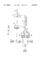
FIG. 1 is a circuit block diagram showing a parallel to serial data converter of a related art. Referring to FIG. 1, the parallel to serial data converter shown has a parallel data input terminal 1. While the parallel data input terminal 1 is provided for n (n is a positive integer) bits, only one input terminal is shown in FIG. 1 for convenience of illustration. The data rate of the parallel data is f bps. The parallel to serial data converter further has a byte clock pulse input terminal 2 for receiving a byte clock pulse signal whose frequency is f and includes an input circuit 3 formed from n flip-flop circuits F/F and driven with the byte clock pulse signal for receiving and latching the parallel data.
The parallel to serial data converter further includes a multiplexer 4 for outputting the parallel data from the input circuit 3 successively and serially one after another one bit. The data rate of the serial output is n·f bps. The parallel to serial data converter further includes a phase-locked loop (PLL) synthesizer 5 for generating a bit clock pulse signal for driving the multiplexer 4. The PLL synthesizer 5 receives the byte clock pulse signal and generates a bit clock pulse signal having a frequency equal to n times the frequency of the byte clock pulse signal, that is, n·f Hz. The parallel to serial data converter further has an output terminal 6 for outputting the serial data from the multiplexer 4. The frequency n·f of the bit clock pulse signal is, for example, 1.25 GHz.
In operation, when n-bit parallel data are inputted via the parallel data input terminal 1 and a byte clock pulse signal is inputted to the byte clock input terminal 2, the parallel data are detected by the input circuit 3 formed from n flip-flops F/F and then inputted to the multiplexer 4. Meanwhile, the PLL synthesizer 5 generates, upon reception of the byte clock pulse signal from the byte clock input terminal 2, a bit clock pulse signal having a frequency n·f equal to n times the frequency of the byte clock pulse signal in synchronism with the byte clock pulse signal and drives the multiplexer 4 with the bit clock pulse signal. Consequently, n-bit parallel data are outputted serially one after another one bit from the multiplexer 4. The data rate then is n·f bps.
The parallel to serial data converter shown in FIG. 1 receives a byte clock pulse signal having a frequency of f Hz as a driving pulse signal, produces, by means of the multiplexer 4 thereof, a bit clock pulse signal having a frequency n·f equal to n times the frequency of the byte clock pulse signal, converts parallel data inputted at the data rate of f bps into serial data at the data rate of n·f bps and outputs the serial data.
By the way, since it is usually required that a parallel to serial data converter operate at a very high rate, it is difficult to use, for a signal processing IC in the preceding stage, a CMOS IC which is used popularly for a signal processing IC, and such a case wherein a bipolar IC or a GaAs semiconductor IC which can operate at a very high rate must be used is progressively increasing.
Since parallel data are usually a non-return to zero (NRZ) signal, the highest operation frequency may be equal to one half frequency f/2 Hz that of the data rate. However, since also a byte clock pulse signal having the frequency f Hz synchronized with the data must be outputted, the operation frequency of the output of the signal processing IC in the preceding stage to the parallel to serial data converter must be equal to the frequency of the data rate after all.
In other words, the data rate of the parallel data relies upon the frequency of the byte clock pulse signal. Further, if a byte clock pulse signal of a high frequency is transmitted, then this makes a noise source. As a result, the parallel to serial data converter is disadvantageous also in that the characteristic of the PLL synthesizer 5 is degraded by the noise and the serial data produced suffer from jitters.
SUMMARY OF THE INVENTION
It is an object of the present invention to provide a parallel to serial data converter which is driven with a comparatively low driving clock pulse signal.
It is another object of the present invention to provide a parallel to serial data converter which eliminates jitters.
In order to attain the objects described above, according to the present invention, there is provided a parallel to serial data converter, comprising an input circuit for latching n-bit parallel data in response to a first control pulse signal, n being a positive integer, a multiplexer for outputting the n-bit parallel data inputted to the input circuit serially one after another one bit in response to a second control pulse signal, a first edge detection circuit for receiving an input clock pulse signal and detecting an edge of each pulse of the input clock pulse signal, a second edge detection circuit for receiving an inverted pulse signal of the input clock pulse signal and detecting an edge of each pulse of the inverted pulse signal, a logic circuit for generating a pulse signal in response to each of detection output pulse signals of the first and second edge detection circuits and outputting the pulse signal as the first control pulse signal to the input circuit, and a pulse generation circuit for receiving the pulse signal of the logic circuit to produce a pulse signal and outputting the pulse signal as the second control pulse signal to the multiplexer.
In the parallel to serial data converter, an edge such as a rising edge or a falling edge of each pulse of an input clock pulse signal and an edge such as a rising edge or a falling edge of each pulse of an inverted pulse signal of the input clock pulse signal are detected, and the logic circuit generates a pulse signal in response to each of the thus detected edges. Then, the pulse signal of the logic circuit is outputted as the first control signal to the input circuit in order to latch input n-bit parallel data and is used for the pulse generation circuit to produce a pulse signal to be outputted as the second control signal to the multiplexer to convert the n-bit parallel data into serial data.
With the parallel to serial data converter, since an edge of each pulse of the input clock pulse signal and an edge of each pulse of the inverted pulse signal of the input clock pulse signal are detected and a pulse signal is generated by the logic circuit each time an edge is detected, the pulse signal generated is synchronized with the input clock pulse signal but has a frequency twice that of the input clock pulse signal. Consequently, the pulse signal from the logic circuit can be used as a byte clock signal, that is, the first control signal, to control the input circuit. Further, the pulse signal of the logic circuit can be inputted to the pulse generation circuit as a pulse signal based on which a bit clock pulse signal, that is, the second control signal, is to be produced.
Accordingly, the input clock pulse signal to be inputted to the parallel to serial data converter may have a frequency equal to one half the data rate of the parallel data, and the operation speed of a signal processing circuit in the preceding stage to the parallel to serial data converter may be reduced to one half comparing with a conventional operation speed. Accordingly, even where conventionally it cannot be avoided to use, for example, a bipolar IC or a GaAs semiconductor IC as a signal processing IC in the preceding stage to the parallel to serial data converter, by applying the present invention, such a case wherein there is no problem even if a CMOS IC is used increases.
Further, since the normal phase and the inverted phase of the same input clock pulse signal are used, noises which are produced when pulses of both of the normal and inverted phases vary cancel each other. As a result, the clock noise is advantageously reduced to a very low level.
Further, although a skew may possibly be produced between the normal phase pulse signal and the opposite phase pulse signal, this does not make a problem if the frequency band of the pulse generation circuit is set to a band which does not respond to the modulation frequency f/2 (f is a data rate of the input parallel data). The reason is that, if the frequency band of the pulse generation circuit is set in this manner, then the pulse generation circuit effects phase modulation with a period of 2T (T=1/f) as seen in FIG. 5 and any phase modulation of such a high modulation frequency is removed by a loop filter or a like element which limits the frequency response band of the pulse generation circuit.
The above and other objects, features and advantages of the present invention will become apparent from the following description and the appended claims, taken in conjunction with the accompanying drawings in which like parts or elements are denoted by like reference characters.
BRIEF DESCRIPTION OF THE DRAWINGS
FIG. 1 is a circuit block diagram showing a parallel to serial data converter of a related art;
FIG. 2A is a circuit block diagram of a parallel to serial data converter showing a first preferred embodiment of the present invention, and FIG. 2B is a timing chart illustrating operation of the parallel to serial data converter of FIG. 2A;
FIG. 3A is a circuit diagram showing a form of rising edge detection circuit of the parallel to serial data converter of FIG. 2A and FIG. 3B is a timing chart illustrating operation of the rising edge detection circuit of FIG. 3A;
FIG. 4A is a circuit diagram showing another form of rising edge detection circuit of the parallel to serial data converter of FIG. 2A and FIG. 4B is a timing chart illustrating operation of the rising edge detection circuit of FIG. 4A; and
FIG. 5 is a timing chart illustrating that operation of a PLL synthesizer of the parallel to serial data converter of FIG. 2A is not influenced by any skew between byte clock pulse signals of the parallel to serial data converter.
DESCRIPTION OF THE PREFERRED EMBODIMENT
Referring first to FIG. 2A, there is shown a parallel to serial data converter to which the present invention is applied. The parallel to serial data converter shown has a parallel data input terminal 11. While the parallel data input terminal 11 is provided for n (n is a positive integer) bits, only one input terminal is shown in FIG. 2A for convenience of illustration. The data rate of the parallel data is f bps. The parallel to serial data converter includes a circuit 17 which produces, from a basic clock pulse signal having a frequency of f/2 Hz, a byte clock pulse signal Byte Clock0 having the same phase as that of the basic clock pulse signal and another byte clock pulse signal Byte Clock1 having an opposite phase inverted from that of the basic clock pulse signal. The byte clock pulse signals Byte Clock0 and Byte Clock1 are inputted to byte clock pulse input terminals 12a and 12b, respectively.
The parallel to serial data converter further includes a pair of rising edge detection circuits 18a and 18b for detecting rising edges of the byte clock pulse signal Byte Clock0 and the byte clock pulse signal Byte Clock1, respectively. Each of the rising edge detection circuits 18a and 18b may have, for example, such a construction as shown in FIG. 3A or 4A. Referring to FIG. 3A, in the rising edge detection circuit shown, the byte clock pulse signal Byte Clock0 (or Byte Clock1) (in FIGS. 3A and 3B, denoted by reference symbol IN) is applied as it is to one of a pair of input terminals of an AND circuit 30 while another signal E obtained by inverting the byte clock pulse signal Byte Clock0 (or Byte Clock1) by means of an invertor 31 and delaying a signal D obtained by the inversion by means of a delay circuit 32 is applied to the other input terminal of the AND circuit 30. Consequently, an output OUT in which a pulse appears at each rising edge of the byte clock pulse signal Byte Clock0 (or Byte Clock1) as seen in FIG. 3B is obtained from the AND circuit 30. It is to be noted that the delay circuit 32 may be formed from, for example, a CR circuit or a cascade connection of a suitable number of stages of gates.
Meanwhile, the rising edge detection circuit shown in FIG. 4A utilizes an output pulse signal of a PLL synthesizer 15, which will be hereinafter described, so that an output OUT in which a pulse appears in synchronism with each rising edge of the byte clock pulse signal Byte Clock0 (or Byte Clock1, denoted by IN in FIGS. 4A and 4B can be obtained as seen in FIG. 5 by flip-flop circuits F/F1 to F/F3 which have a clear terminal.
It is to be noted that, while rising edges of the byte clock pulse signals Byte Clock0 and Byte Clock1 are detected in the present embodiment, the object of the detection is not limited to them, and falling edges may be detected alternatively.
Referring back to FIG. 2A, the parallel to serial data converter further includes a logical OR circuit 19 which receives outputs 1 and 2 of the rising edge detection circuits 18a and 18b and whose output 3 serves as a byte clock pulse signal of a frequency f Hz. The parallel to serial data converter further includes an input circuit 13 formed from n flip-flop circuits F/F for receiving and latching parallel data. The input circuit 13 is driven with the byte clock pulse signal 3 whose frequency is f Hz. The parallel to serial data converter further includes a multiplexer 14 which outputs parallel data from the input circuit 13 successively and serially one after another one bit. The data rate then is n·f bps. The parallel to serial data converter further includes a PLL synthesizer 15 for generating a bit clock pulse signal for driving the multiplexer 14. The PLL synthesizer 15 receives the byte clock pulse signal 3 and generates a bit clock pulse signal having a frequency of n·f Hz equal to n times that of the byte clock pulse signal 3. The parallel to serial data converter further has an output terminal 16 for outputting serial data from the multiplexer 14.
In operation, n-bit (for example, n=10 as a result of 8b/10b conversion by, for example, a CMOS IC in the preceding stage) are inputted via the parallel data input terminal 11. Meanwhile, a byte clock pulse signal Byte Clock0 whose frequency is f/2 is inputted via the byte clock pulse input terminal 12a while another byte clock pulse signal Byte Clock1 whose frequency is f/2 is inputted via the byte clock pulse input terminal 12b. The byte clock pulse signals Byte Clock0 and Byte Clock1 are inputted to the rising edge detection circuits 18a and 18b, respectively. Consequently, a pulse signal 1 which is generated at each rising edge of the byte clock pulse signal Byte Clock0 and another pulse signal 2 which is generated at each rising edge of the byte clock pulse signal Byte Clock1 are outputted from the rising edge detection circuits 18a and 18b, respectively. The pulse signals 1 and 2 are inputted to the logical OR circuit 19, and from the logical OR circuit 19, a byte clock pulse signal 3 is outputted. The byte clock pulse signal 3 is a pulse signal corresponding to the byte clock pulse signal of the parallel to serial data converter described hereinabove with reference to FIG. 1. The byte clock pulse signal 3 is applied as a driving pulse signal to the input circuit 13 which is formed from n flip-flops F/F.
Meanwhile, the parallel data inputted from the parallel data input terminal 11 are fetched by the input circuit 13 and then inputted to the multiplexer 14. Then, the PLL synthesizer 15 generates, when the byte clock pulse signal 3 is received, a bit clock pulse signal having a frequency n·f equal to n times that of the byte clock pulse signal 3 in synchronism with the byte clock pulse signal 3 and drives the multiplexer 14 with the bit clock pulse signal. Consequently, the n-bit parallel data are outputted serially one after another one bit from the multiplexer 14. The data rate then is n·f bps, for example, 1.25 Gbps.
In this manner, the parallel to serial data converter shown in FIG. 2A receives a clock pulse signal whose frequency is f/2 Hz as a driving pulse signal, produces byte clock pulse signals Byte Clock0 and Byte Clock1 of f Hz, further produces a byte clock pulse signal 3 of f Hz from the byte clock pulse signals Byte Clock0 and Byte Clock1, drives the input circuit 13 with the byte clock pulse signal 3 and applies the byte clock pulse signal 3 to the PLL synthesizer 15. The PLL synthesizer 15 receives the byte clock pulse signal 3 and produces, based on the byte clock pulse signal 3, a bit clock pulse signal having a frequency n·f equal to n times that of the byte clock pulse signal 3. Further, the PLL synthesizer 15 converts the parallel data inputted thereto at the data rate of f bps into serial data at the data rate of n·f bps and outputs the serial data.
Accordingly, the driving basic clock pulse signal to be inputted to the parallel to serial data converter may have a frequency equal to one half the data rate of the parallel data, and the operation speed of a signal processing circuit in the preceding stage to the parallel to serial data converter may be reduced to one half comparing with a conventional operation speed. Accordingly, even where conventionally it cannot be avoided to use, for example, a bipolar IC or a GaAs semiconductor IC as a signal processing IC in the preceding stage to the parallel to serial data converter, application of the present invention increases a case wherein there is no problem even if a CMOS IC is used.
Incidentally, it may be considered that an interleaving technique may possibly be used such that, using two inputting elements which operate with a driving frequency of f/2 bps, parallel data are inputted to the two byte clock pulse input terminals 12 and one of the byte clock pulse input terminals 12 is driven with the byte clock pulse signal Byte Clock0 while the other byte clock pulse input terminal 12 is driven with the byte clock pulse signal Byte Clock1 so that the parallel data are shifted by the multiplexer 14 to convert them into serial data. This reduces the frequency of the basic pulse signal to be inputted to the parallel to serial data converter to f/2, similarly to the parallel to serial data converter of the present embodiment. However, such employment of the interleaving technique in the parallel to serial data converter increases the bit width of data to twice and is not the best plan since the number of elements is increased such that the number of flip-flops must be increased to twice and this gives rise to an increase in power dissipation.
Further, with the parallel to serial data converter of the present embodiment, since the normal phase and the inverted phase of the same basic clock pulse signal are used, noises which are produced when pulses of both of the normal and inverted phases vary (rise or fall) cancel each other. As a result, the clock noise is advantageously reduced to a very low level.
Further, although a skew may possibly be produced between the normal phase byte clock pulse signal Byte Clock0 and the opposite phase byte clock pulse signal Byte Clock1, this does not make a problem if the frequency band of the PLL synthesizer is set to a band which does not respond to the modulation frequency f/2. FIG. 5 is a timing chart illustrating this.
In particular, although a skew Tskew may possibly be produced between the byte clock pulse signal Byte Clock0 and the byte clock pulse signal Byte Clock1, such skew Tskew is produced once per one period 2T. Accordingly, if the frequency band of the PLL synthesizer 15 is set to a band which does not respond to the modulation frequency f/2, then any phase modulation of such a high modulation frequency is removed by a loop filter or a like element which limits the frequency response band of the PLL synthesizer so that the PLL synthesizer 15 may not be influenced by the skew at all.
With the parallel to serial data converter of the present invention, since a rising edge (or a falling edge) of each pulse of the basic clock pulse signal and a rising edge (or a falling edge) of each pulse of an inverted pulse signal of the basic clock pulse signal are detected and a pulse signal can be generated each time an edge is detected, the pulse signal obtained is synchronized with the basic clock pulse signal but has a frequency twice that of the basic clock pulse signal. Consequently, the pulse signal can be used as a byte clock signal to control the input circuit and besides can be inputted as a pulse signal, based on which a bit clock pulse signal is to be produced, to the pulse generation circuit.
Accordingly, the driving basic clock pulse signal to be inputted to the parallel to serial data converter may have a frequency equal to one half the data rate of the parallel data, and the operation speed of a signal processing circuit in the preceding stage to the parallel to serial data converter may be reduced to one half comparing with a conventional operation speed. Accordingly, even where conventionally it cannot be avoided to use, for example, a bipolar IC or a GaAs semiconductor IC as a signal processing IC in the preceding stage to the parallel to serial data converter, if the present invention is applied, then such a case wherein there is no problem even if a CMOS IC is used increases.
Further, since the normal phase and the inverted phase of the same basic clock pulse signal are used, noises which are produced when pulses of both of the normal and inverted phases vary cancel each other. As a result, the clock noise is advantageously reduced to a very low level.
Further, although a skew may possibly be produced between the normal phase pulse signal and the opposite phase pulse signal, this does not make a problem if the frequency band of the PLL synthesizer is set to a band which does not respond to the modulation frequency f/2. The reason is that, if the frequency band of the PLL synthesizer is set in this manner, then the PLL circuit effects phase modulation with a period of 2T (T=1/f) as seen in FIG. 5 and any phase modulation of such a high modulation frequency is removed by a loop filter or a like element which limits the frequency response band of the PLL synthesizer thereby to eliminate the screw.

Claims (10)

What is claimed is:
1. A parallel to serial data converter, comprising:
an input circuit for latching n-bit parallel data in response to a first control pulse signal, n being a positive integer;
a multiplexer for outputting the n-bit parallel data inputted to said input circuit serially one after another one bit in response to a second control pulse signal;
a first edge detection circuit for receiving an input clock pulse signal and detecting an edge of each pulse of the input clock pulse signal;
a second edge detection circuit for receiving an inverted pulse signal of the input clock pulse signal and detecting an edge of each pulse of the inverted pulse signal;
a logic circuit for generating a pulse signal in response to each of detection output pulse signals of said first and second edge detection circuits and outputting the pulse signal as the first control pulse signal to said input circuit; and
a pulse generation circuit for receiving the pulse signal of said logic circuit to produce a pulse signal and outputting the pulse signal as the second control pulse signal to said multiplexer.
2. A parallel to serial data converter according to claim 1, wherein the input clock pulse signal has a data rate set lower than that of the parallel data.
3. A parallel to serial data converter according to claim 2, wherein the input clock pulse signal has a data rate set to one half that of the parallel data.
4. A parallel to serial data converter according to claim 2, wherein said clock pulse generation circuit is formed from a phase-locked loop synthesizer whose frequency band is set to a low band which does not respond to the frequency of the byte clock pulse signal outputted from said logic circuit.
5. A parallel to serial data converter according to claim 1, wherein said first and second edge detection circuits detect a rising or falling edge of each pulse of the input clock pulse signal.
6. A parallel to serial data converter according to claim 1, wherein said logic circuit which generates the output pulse signal is a logical OR circuit.
7. A parallel to serial data converter, comprising:
an input circuit for latching n-bit parallel data in response to a first control pulse signal, n being a positive integer;
a multiplexer for outputting the n-bit parallel data inputted to said input circuit serially one after another one bit in response to a second control pulse signal;
a first edge detection circuit for receiving an input clock pulse signal and detecting a rising edge or a falling edge of each pulse of the input clock pulse signal;
a second edge detection circuit for receiving an inverted pulse signal of the input clock pulse signal and detecting that one of a rising edge and a falling edge of each pulse of the inverted pulse signal which is detected by said first edge detection circuit;
a logical OR circuit for detection outputs of said first and second edge detection circuits to produce a pulse signal and outputting the pulse signal as the first control pulse signal to said input circuit; and
a pulse generation circuit for receiving the pulse signal of said logic circuit to produce a pulse signal and outputting the pulse signal as the second control pulse signal to said multiplexer.
8. A parallel to serial data converter according to claim 7, wherein the input clock pulse signal has a data rate set lower than that of the parallel data.
9. A parallel to serial data converter according to claim 7, wherein the input clock pulse signal has a data rate set to one half that of the parallel data.
10. A parallel to serial data converter according to claim 7, wherein said clock pulse generation circuit is formed from a phase-locked loop synthesizer whose frequency band is set to a low band which does not respond to the frequency of the byte clock pulse signal outputted from said logic circuit.
US08/848,632 1996-05-14 1997-04-29 Parallel to serial data converter Expired - Fee Related US5798720A (en)

Applications Claiming Priority (2)

Application Number Priority Date Filing Date Title
JP8-119166 1996-05-14
JP8119166A JPH09307457A (en) 1996-05-14 1996-05-14 Parallel/serial conversion circuit

Publications (1)

Publication Number Publication Date
US5798720A true US5798720A (en) 1998-08-25

Family

ID=14754552

Family Applications (1)

Application Number Title Priority Date Filing Date
US08/848,632 Expired - Fee Related US5798720A (en) 1996-05-14 1997-04-29 Parallel to serial data converter

Country Status (2)

Country Link
US (1) US5798720A (en)
JP (1) JPH09307457A (en)

Cited By (43)

* Cited by examiner, † Cited by third party
Publication number Priority date Publication date Assignee Title
US5982309A (en) * 1998-01-09 1999-11-09 Iowa State University Research Foundation, Inc. Parallel-to-serial CMOS data converter with a selectable bit width mode D flip-flop M matrix
US20010054122A1 (en) * 2000-06-16 2001-12-20 Fujitsu Limited Data burst transfer circuit, parallel-serial and serial-parallel conversion circuits, and an oscillation circuit
US6335696B1 (en) * 2000-05-10 2002-01-01 Mitsubishi Denki Kabushiki Kaisha Parallel-serial conversion circuit
US20030007162A1 (en) * 2001-06-29 2003-01-09 Marc Blumer Digital pulse width modulator for use in electrostatic printing mechanisms
US6657623B1 (en) * 1999-07-13 2003-12-02 Samsung Electronics Co., Ltd. Method and apparatus for transmitting a video signal
US6686856B1 (en) * 2002-11-20 2004-02-03 Agilent Technologies, Inc. Clocking domain conversion system and method
US20050062864A1 (en) * 2003-09-04 2005-03-24 Keiji Mabuchi Solid-state image sensing apparatus
US20050225642A1 (en) * 2004-04-10 2005-10-13 Leica Microsystems Semiconductor Gmbh Apparatus and method for the determination of positioning coordinates for semiconductor substrates
US20060104124A1 (en) * 2004-11-16 2006-05-18 Padaparambil Muralikumar A Dual-edge triggered multiplexer flip-flop and method
US20060103557A1 (en) * 2004-11-16 2006-05-18 Padaparambil Muralikumar A Low-power serializer with half-rate clocking and method
US20060192699A1 (en) * 1999-01-28 2006-08-31 Semiconductor Energy Laboratory Co., Ltd. Serial-to-parallel conversion circuit, and semiconductor display device employing the same
US7295554B1 (en) * 1999-03-12 2007-11-13 Lucent Technologies Inc. Word Multiplexing of encoded signals into a higher bit rate serial data stream
US20100289677A1 (en) * 2009-05-18 2010-11-18 Choi Chang-Kyu Circuit and method for parallel to serial conversion
US20110123201A1 (en) * 2008-08-22 2011-05-26 Omron Corporation Parallel-serial converter for optical transmission, optical transmission system, and electronic apparatus
US8539119B2 (en) 2004-11-24 2013-09-17 Qualcomm Incorporated Methods and apparatus for exchanging messages having a digital data interface device message format
US8606946B2 (en) 2003-11-12 2013-12-10 Qualcomm Incorporated Method, system and computer program for driving a data signal in data interface communication data link
US8611215B2 (en) 2005-11-23 2013-12-17 Qualcomm Incorporated Systems and methods for digital data transmission rate control
US8624761B1 (en) * 2010-04-27 2014-01-07 Southern Methodist University Serializing parallel data streams
US8625625B2 (en) 2004-03-10 2014-01-07 Qualcomm Incorporated High data rate interface apparatus and method
US8630318B2 (en) 2004-06-04 2014-01-14 Qualcomm Incorporated High data rate interface apparatus and method
US8635358B2 (en) 2003-09-10 2014-01-21 Qualcomm Incorporated High data rate interface
US8645566B2 (en) 2004-03-24 2014-02-04 Qualcomm Incorporated High data rate interface apparatus and method
US8650304B2 (en) 2004-06-04 2014-02-11 Qualcomm Incorporated Determining a pre skew and post skew calibration data rate in a mobile display digital interface (MDDI) communication system
US8667363B2 (en) 2004-11-24 2014-03-04 Qualcomm Incorporated Systems and methods for implementing cyclic redundancy checks
US8670457B2 (en) 2003-12-08 2014-03-11 Qualcomm Incorporated High data rate interface with improved link synchronization
US8681817B2 (en) 2003-06-02 2014-03-25 Qualcomm Incorporated Generating and implementing a signal protocol and interface for higher data rates
US8687658B2 (en) 2003-11-25 2014-04-01 Qualcomm Incorporated High data rate interface with improved link synchronization
US8694663B2 (en) 2001-09-06 2014-04-08 Qualcomm Incorporated System for transferring digital data at a high rate between a host and a client over a communication path for presentation to a user
US8694652B2 (en) 2003-10-15 2014-04-08 Qualcomm Incorporated Method, system and computer program for adding a field to a client capability packet sent from a client to a host
US8692838B2 (en) 2004-11-24 2014-04-08 Qualcomm Incorporated Methods and systems for updating a buffer
US8692839B2 (en) 2005-11-23 2014-04-08 Qualcomm Incorporated Methods and systems for updating a buffer
US8705571B2 (en) 2003-08-13 2014-04-22 Qualcomm Incorporated Signal interface for higher data rates
US8705521B2 (en) 2004-03-17 2014-04-22 Qualcomm Incorporated High data rate interface apparatus and method
US8723705B2 (en) 2004-11-24 2014-05-13 Qualcomm Incorporated Low output skew double data rate serial encoder
US8730069B2 (en) 2005-11-23 2014-05-20 Qualcomm Incorporated Double data rate serial encoder
US8745251B2 (en) 2000-12-15 2014-06-03 Qualcomm Incorporated Power reduction system for an apparatus for high data rate signal transfer using a communication protocol
US8756294B2 (en) 2003-10-29 2014-06-17 Qualcomm Incorporated High data rate interface
US8760328B1 (en) 2012-09-14 2014-06-24 Altera Corporation Interface circuitry for an integrated circuit system
US8873584B2 (en) 2004-11-24 2014-10-28 Qualcomm Incorporated Digital data interface device
US8947734B1 (en) * 2006-07-27 2015-02-03 Marvell International Ltd. Pulse width modulator for a printing device
ITRM20130704A1 (en) * 2013-12-20 2015-06-21 Intecs S P A METHOD AND TIMING COMMUNICATION SYSTEM WITH PHASE COHERENCE BETWEEN REMOTE CONNECTED SYSTEMS THROUGH OPTICAL OR ELECTRIC HIGH SPEED DATA LINE
US9479148B2 (en) * 2015-02-26 2016-10-25 Lenovo Enterprise Solutions (Singapore) Pte. Ltd. Serial data signal edge detection
US11615824B2 (en) 2021-04-28 2023-03-28 Samsung Electronics Co., Ltd. Serializer and memory device including the same

Families Citing this family (6)

* Cited by examiner, † Cited by third party
Publication number Priority date Publication date Assignee Title
JP3739024B2 (en) * 1998-01-23 2006-01-25 富士フイルムマイクロデバイス株式会社 Differential logic circuit for parallel-serial conversion
JP4099255B2 (en) * 1998-01-28 2008-06-11 富士通株式会社 Dry cell housing structure and electronic device having the same
JP4412788B2 (en) * 2000-01-24 2010-02-10 株式会社ルネサステクノロジ Parallel-serial conversion circuit
WO2002065688A1 (en) 2001-02-16 2002-08-22 Fujitsu Limited Timing extracting circuit of optical receiver using frequency clock that is half the data transmission rate, and duty shift adaptive circuit of optical transceiver
CN101444027B (en) * 2004-11-24 2013-03-20 高通股份有限公司 Systems and methods for implementation of cyclic redundancy check
WO2019003588A1 (en) * 2017-06-29 2019-01-03 パナソニックIpマネジメント株式会社 Noise cancel circuit and data transmission circuit

Citations (7)

* Cited by examiner, † Cited by third party
Publication number Priority date Publication date Assignee Title
US4752942A (en) * 1984-01-09 1988-06-21 Nec Corporation Method and circuitry for extracting clock signal from received biphase modulated signal
US5012240A (en) * 1988-12-28 1991-04-30 Nippon Hoso Kyokai Parallel to serial converter with complementary bit insertion for disparity reduction
US5548285A (en) * 1994-07-18 1996-08-20 Motorola, Inc. Circuit and method of indicating data hold-time
US5548622A (en) * 1995-03-24 1996-08-20 Sgs-Thomson Microelectronics, Inc. Method and structure for synchronization of asynchronous signals
US5563594A (en) * 1994-08-31 1996-10-08 Motorola Circuit and method of timing data transfers
US5627828A (en) * 1994-03-15 1997-05-06 Lg Semicon Co., Ltd. Method and circuit for detecting data collisions in communication network
US5714904A (en) * 1994-06-06 1998-02-03 Sun Microsystems, Inc. High speed serial link for fully duplexed data communication

Patent Citations (7)

* Cited by examiner, † Cited by third party
Publication number Priority date Publication date Assignee Title
US4752942A (en) * 1984-01-09 1988-06-21 Nec Corporation Method and circuitry for extracting clock signal from received biphase modulated signal
US5012240A (en) * 1988-12-28 1991-04-30 Nippon Hoso Kyokai Parallel to serial converter with complementary bit insertion for disparity reduction
US5627828A (en) * 1994-03-15 1997-05-06 Lg Semicon Co., Ltd. Method and circuit for detecting data collisions in communication network
US5714904A (en) * 1994-06-06 1998-02-03 Sun Microsystems, Inc. High speed serial link for fully duplexed data communication
US5548285A (en) * 1994-07-18 1996-08-20 Motorola, Inc. Circuit and method of indicating data hold-time
US5563594A (en) * 1994-08-31 1996-10-08 Motorola Circuit and method of timing data transfers
US5548622A (en) * 1995-03-24 1996-08-20 Sgs-Thomson Microelectronics, Inc. Method and structure for synchronization of asynchronous signals

Cited By (71)

* Cited by examiner, † Cited by third party
Publication number Priority date Publication date Assignee Title
US5982309A (en) * 1998-01-09 1999-11-09 Iowa State University Research Foundation, Inc. Parallel-to-serial CMOS data converter with a selectable bit width mode D flip-flop M matrix
US20060192699A1 (en) * 1999-01-28 2006-08-31 Semiconductor Energy Laboratory Co., Ltd. Serial-to-parallel conversion circuit, and semiconductor display device employing the same
KR100837585B1 (en) * 1999-01-28 2008-06-13 가부시키가이샤 한도오따이 에네루기 켄큐쇼 Serial-to-parallel conversion circuit, and semiconductor display device employing the same
US7355534B2 (en) 1999-01-28 2008-04-08 Semiconductor Energy Laboratory Co., Ltd. Serial-to-parallel conversion circuit, and semiconductor display device employing the same
US7295554B1 (en) * 1999-03-12 2007-11-13 Lucent Technologies Inc. Word Multiplexing of encoded signals into a higher bit rate serial data stream
US6657623B1 (en) * 1999-07-13 2003-12-02 Samsung Electronics Co., Ltd. Method and apparatus for transmitting a video signal
US6335696B1 (en) * 2000-05-10 2002-01-01 Mitsubishi Denki Kabushiki Kaisha Parallel-serial conversion circuit
US20010054122A1 (en) * 2000-06-16 2001-12-20 Fujitsu Limited Data burst transfer circuit, parallel-serial and serial-parallel conversion circuits, and an oscillation circuit
US6701396B2 (en) * 2000-06-16 2004-03-02 Fujitsu Limited Data burst transfer circuit, parallel-serial and serial-parallel conversion circuits, and an oscillation circuit
US20040150539A1 (en) * 2000-06-16 2004-08-05 Fujitsu Limited Data burst transfer circuit, parallel-serial and serial-parallel conversion circuits, and an oscillation circuit
US6928496B2 (en) * 2000-06-16 2005-08-09 Fujitsu Limited Data burst transfer circuit, parallel-serial and serial-parallel conversion circuits, and an oscillation circuit
US8745251B2 (en) 2000-12-15 2014-06-03 Qualcomm Incorporated Power reduction system for an apparatus for high data rate signal transfer using a communication protocol
US7453596B2 (en) * 2001-06-29 2008-11-18 Electronics For Imaging, Inc. Digital pulse width modulator for use in electrostatic printing mechanisms
US6992792B2 (en) * 2001-06-29 2006-01-31 Electronics For Imaging, Inc. Digital pulse width modulator for use in electrostatic printing mechanisms
US20030007162A1 (en) * 2001-06-29 2003-01-09 Marc Blumer Digital pulse width modulator for use in electrostatic printing mechanisms
US20060087693A1 (en) * 2001-06-29 2006-04-27 Electronics For Imaging, Inc. Digital pulse width modulator for use in electrostatic printing mechanisms
WO2003003713A1 (en) * 2001-06-29 2003-01-09 Electronics For Imaging, Inc. Digital pulse width modulator for use in electrostatic printing mechanisms
US8812706B1 (en) 2001-09-06 2014-08-19 Qualcomm Incorporated Method and apparatus for compensating for mismatched delays in signals of a mobile display interface (MDDI) system
US8694663B2 (en) 2001-09-06 2014-04-08 Qualcomm Incorporated System for transferring digital data at a high rate between a host and a client over a communication path for presentation to a user
US6686856B1 (en) * 2002-11-20 2004-02-03 Agilent Technologies, Inc. Clocking domain conversion system and method
US8681817B2 (en) 2003-06-02 2014-03-25 Qualcomm Incorporated Generating and implementing a signal protocol and interface for higher data rates
US8700744B2 (en) 2003-06-02 2014-04-15 Qualcomm Incorporated Generating and implementing a signal protocol and interface for higher data rates
US8705579B2 (en) 2003-06-02 2014-04-22 Qualcomm Incorporated Generating and implementing a signal protocol and interface for higher data rates
US8705571B2 (en) 2003-08-13 2014-04-22 Qualcomm Incorporated Signal interface for higher data rates
US20050062864A1 (en) * 2003-09-04 2005-03-24 Keiji Mabuchi Solid-state image sensing apparatus
US20120268636A1 (en) * 2003-09-04 2012-10-25 Sony Corporation Solid-state image sensing apparatus
US9060126B2 (en) * 2003-09-04 2015-06-16 Sony Corporation Solid-state image sensing apparatus
US10212377B2 (en) * 2003-09-04 2019-02-19 Sony Corporation Solid-state image sensing apparatus
US9648264B2 (en) * 2003-09-04 2017-05-09 Sony Corporation Solid-state image sensing apparatus
US20150271404A1 (en) * 2003-09-04 2015-09-24 Sony Corporation Solid-state image sensing apparatus
US20150237288A1 (en) * 2003-09-04 2015-08-20 Sony Corporation Solid-state image sensing apparatus
US8635358B2 (en) 2003-09-10 2014-01-21 Qualcomm Incorporated High data rate interface
US8719334B2 (en) 2003-09-10 2014-05-06 Qualcomm Incorporated High data rate interface
US8694652B2 (en) 2003-10-15 2014-04-08 Qualcomm Incorporated Method, system and computer program for adding a field to a client capability packet sent from a client to a host
US8756294B2 (en) 2003-10-29 2014-06-17 Qualcomm Incorporated High data rate interface
US8606946B2 (en) 2003-11-12 2013-12-10 Qualcomm Incorporated Method, system and computer program for driving a data signal in data interface communication data link
US8687658B2 (en) 2003-11-25 2014-04-01 Qualcomm Incorporated High data rate interface with improved link synchronization
US8670457B2 (en) 2003-12-08 2014-03-11 Qualcomm Incorporated High data rate interface with improved link synchronization
US8669988B2 (en) 2004-03-10 2014-03-11 Qualcomm Incorporated High data rate interface apparatus and method
US8625625B2 (en) 2004-03-10 2014-01-07 Qualcomm Incorporated High data rate interface apparatus and method
US8730913B2 (en) 2004-03-10 2014-05-20 Qualcomm Incorporated High data rate interface apparatus and method
US8705521B2 (en) 2004-03-17 2014-04-22 Qualcomm Incorporated High data rate interface apparatus and method
US8645566B2 (en) 2004-03-24 2014-02-04 Qualcomm Incorporated High data rate interface apparatus and method
US20050225642A1 (en) * 2004-04-10 2005-10-13 Leica Microsystems Semiconductor Gmbh Apparatus and method for the determination of positioning coordinates for semiconductor substrates
US8630318B2 (en) 2004-06-04 2014-01-14 Qualcomm Incorporated High data rate interface apparatus and method
US8650304B2 (en) 2004-06-04 2014-02-11 Qualcomm Incorporated Determining a pre skew and post skew calibration data rate in a mobile display digital interface (MDDI) communication system
US8630305B2 (en) 2004-06-04 2014-01-14 Qualcomm Incorporated High data rate interface apparatus and method
US20060104124A1 (en) * 2004-11-16 2006-05-18 Padaparambil Muralikumar A Dual-edge triggered multiplexer flip-flop and method
US7079055B2 (en) 2004-11-16 2006-07-18 Seiko Epson Corporation Low-power serializer with half-rate clocking and method
US7161846B2 (en) 2004-11-16 2007-01-09 Seiko Epson Corporation Dual-edge triggered multiplexer flip-flop and method
US20060103557A1 (en) * 2004-11-16 2006-05-18 Padaparambil Muralikumar A Low-power serializer with half-rate clocking and method
US8539119B2 (en) 2004-11-24 2013-09-17 Qualcomm Incorporated Methods and apparatus for exchanging messages having a digital data interface device message format
US8873584B2 (en) 2004-11-24 2014-10-28 Qualcomm Incorporated Digital data interface device
US8723705B2 (en) 2004-11-24 2014-05-13 Qualcomm Incorporated Low output skew double data rate serial encoder
US8699330B2 (en) 2004-11-24 2014-04-15 Qualcomm Incorporated Systems and methods for digital data transmission rate control
US8692838B2 (en) 2004-11-24 2014-04-08 Qualcomm Incorporated Methods and systems for updating a buffer
US8667363B2 (en) 2004-11-24 2014-03-04 Qualcomm Incorporated Systems and methods for implementing cyclic redundancy checks
US8730069B2 (en) 2005-11-23 2014-05-20 Qualcomm Incorporated Double data rate serial encoder
US8611215B2 (en) 2005-11-23 2013-12-17 Qualcomm Incorporated Systems and methods for digital data transmission rate control
US8692839B2 (en) 2005-11-23 2014-04-08 Qualcomm Incorporated Methods and systems for updating a buffer
US9361556B1 (en) 2006-07-27 2016-06-07 Marvell International Ltd. Pulse width modulator for a printing device
US8947734B1 (en) * 2006-07-27 2015-02-03 Marvell International Ltd. Pulse width modulator for a printing device
US20110123201A1 (en) * 2008-08-22 2011-05-26 Omron Corporation Parallel-serial converter for optical transmission, optical transmission system, and electronic apparatus
US8467689B2 (en) * 2008-08-22 2013-06-18 Omron Corporation Parallel-serial converter for optical transmission, optical transmission system, and electronic apparatus
US20100289677A1 (en) * 2009-05-18 2010-11-18 Choi Chang-Kyu Circuit and method for parallel to serial conversion
US8106798B2 (en) * 2009-05-18 2012-01-31 Hynix Semiconductor Inc. Circuit and method for parallel to serial conversion
US8624761B1 (en) * 2010-04-27 2014-01-07 Southern Methodist University Serializing parallel data streams
US8760328B1 (en) 2012-09-14 2014-06-24 Altera Corporation Interface circuitry for an integrated circuit system
ITRM20130704A1 (en) * 2013-12-20 2015-06-21 Intecs S P A METHOD AND TIMING COMMUNICATION SYSTEM WITH PHASE COHERENCE BETWEEN REMOTE CONNECTED SYSTEMS THROUGH OPTICAL OR ELECTRIC HIGH SPEED DATA LINE
US9479148B2 (en) * 2015-02-26 2016-10-25 Lenovo Enterprise Solutions (Singapore) Pte. Ltd. Serial data signal edge detection
US11615824B2 (en) 2021-04-28 2023-03-28 Samsung Electronics Co., Ltd. Serializer and memory device including the same

Also Published As

Publication number Publication date
JPH09307457A (en) 1997-11-28

Similar Documents

Publication Publication Date Title
US5798720A (en) Parallel to serial data converter
US11005466B2 (en) Measurement and correction of multiphase clock duty cycle and skew
US7590208B2 (en) Circuit and method for generating a timing signal, and signal transmission system performing for high-speed signal transmission and reception between LSIs
US5592125A (en) Modified bang-bang phase detector with ternary output
US5412697A (en) Delay line separator for data bus
US6292040B1 (en) Internal clock signal generating circuit having function of generating internal clock signals which are multiplication of an external clock signal
US6710726B2 (en) Serializer-deserializer circuit having increased margins for setup and hold time
US5887040A (en) High speed digital data retiming apparatus
US6225831B1 (en) Phase detector
US6236697B1 (en) Clock recovery for multiple frequency input data
US7482841B1 (en) Differential bang-bang phase detector (BBPD) with latency reduction
JP3094971B2 (en) Phase comparison circuit, phase-locked loop circuit and serial-parallel conversion circuit using the same
JPH07131448A (en) Phase comparing circuit
US6700944B1 (en) Phase detector for clock and data recovery
US6298104B1 (en) Clock recovery circuit
US4686482A (en) Clock signal arrangement for regenerating a clock signal
JP2805604B2 (en) Manchester code decoding device
US5306959A (en) Electrical circuit for generating pulse strings
JP3942475B2 (en) Clock recovery circuit and data receiving circuit
US7257184B2 (en) Phase comparator, clock data recovery circuit and transceiver circuit
US20040190667A1 (en) Clock extracting circuit and clock extracting method
US4818894A (en) Method and apparatus for obtaining high frequency resolution of a low frequency signal
KR100212551B1 (en) An improved apparatus for generating sync-clock of video signals
KR940004997Y1 (en) Error detecting apparatus of digital data signal
JPH1168861A (en) Simultaneous two-way transmission reception method and simultaneous two-way transmission reception circuit

Legal Events

Date Code Title Description
AS Assignment

Owner name: SONY CORPORATION, JAPAN

Free format text: ASSIGNMENT OF ASSIGNORS INTEREST;ASSIGNOR:YANO, MOTOYASU;REEL/FRAME:008540/0440

Effective date: 19970417

FEPP Fee payment procedure

Free format text: PAYOR NUMBER ASSIGNED (ORIGINAL EVENT CODE: ASPN); ENTITY STATUS OF PATENT OWNER: LARGE ENTITY

FPAY Fee payment

Year of fee payment: 4

FPAY Fee payment

Year of fee payment: 8

REMI Maintenance fee reminder mailed
LAPS Lapse for failure to pay maintenance fees

Free format text: PATENT EXPIRED FOR FAILURE TO PAY MAINTENANCE FEES (ORIGINAL EVENT CODE: EXP.); ENTITY STATUS OF PATENT OWNER: LARGE ENTITY

STCH Information on status: patent discontinuation

Free format text: PATENT EXPIRED DUE TO NONPAYMENT OF MAINTENANCE FEES UNDER 37 CFR 1.362

FP Lapsed due to failure to pay maintenance fee

Effective date: 20100825