US5879783A - Low noise magnetic recording medium and method of manufacturing - Google Patents
Low noise magnetic recording medium and method of manufacturing Download PDFInfo
- Publication number
- US5879783A US5879783A US08/735,443 US73544397A US5879783A US 5879783 A US5879783 A US 5879783A US 73544397 A US73544397 A US 73544397A US 5879783 A US5879783 A US 5879783A
- Authority
- US
- United States
- Prior art keywords
- seed layer
- magnetic
- underlayer
- recording medium
- magnetic recording
- Prior art date
- Legal status (The legal status is an assumption and is not a legal conclusion. Google has not performed a legal analysis and makes no representation as to the accuracy of the status listed.)
- Expired - Lifetime
Links
Images


Classifications
-
- G—PHYSICS
- G11—INFORMATION STORAGE
- G11B—INFORMATION STORAGE BASED ON RELATIVE MOVEMENT BETWEEN RECORD CARRIER AND TRANSDUCER
- G11B5/00—Recording by magnetisation or demagnetisation of a record carrier; Reproducing by magnetic means; Record carriers therefor
- G11B5/84—Processes or apparatus specially adapted for manufacturing record carriers
- G11B5/8404—Processes or apparatus specially adapted for manufacturing record carriers manufacturing base layers
-
- G—PHYSICS
- G11—INFORMATION STORAGE
- G11B—INFORMATION STORAGE BASED ON RELATIVE MOVEMENT BETWEEN RECORD CARRIER AND TRANSDUCER
- G11B5/00—Recording by magnetisation or demagnetisation of a record carrier; Reproducing by magnetic means; Record carriers therefor
- G11B5/62—Record carriers characterised by the selection of the material
- G11B5/73—Base layers, i.e. all non-magnetic layers lying under a lowermost magnetic recording layer, e.g. including any non-magnetic layer in between a first magnetic recording layer and either an underlying substrate or a soft magnetic underlayer
- G11B5/7368—Non-polymeric layer under the lowermost magnetic recording layer
- G11B5/7369—Two or more non-magnetic underlayers, e.g. seed layers or barrier layers
- G11B5/737—Physical structure of underlayer, e.g. texture
-
- G—PHYSICS
- G11—INFORMATION STORAGE
- G11B—INFORMATION STORAGE BASED ON RELATIVE MOVEMENT BETWEEN RECORD CARRIER AND TRANSDUCER
- G11B5/00—Recording by magnetisation or demagnetisation of a record carrier; Reproducing by magnetic means; Record carriers therefor
- G11B5/62—Record carriers characterised by the selection of the material
- G11B5/73—Base layers, i.e. all non-magnetic layers lying under a lowermost magnetic recording layer, e.g. including any non-magnetic layer in between a first magnetic recording layer and either an underlying substrate or a soft magnetic underlayer
- G11B5/7368—Non-polymeric layer under the lowermost magnetic recording layer
- G11B5/7379—Seed layer, e.g. at least one non-magnetic layer is specifically adapted as a seed or seeding layer
-
- G—PHYSICS
- G11—INFORMATION STORAGE
- G11B—INFORMATION STORAGE BASED ON RELATIVE MOVEMENT BETWEEN RECORD CARRIER AND TRANSDUCER
- G11B5/00—Recording by magnetisation or demagnetisation of a record carrier; Reproducing by magnetic means; Record carriers therefor
- G11B5/62—Record carriers characterised by the selection of the material
- G11B5/73—Base layers, i.e. all non-magnetic layers lying under a lowermost magnetic recording layer, e.g. including any non-magnetic layer in between a first magnetic recording layer and either an underlying substrate or a soft magnetic underlayer
- G11B5/739—Magnetic recording media substrates
- G11B5/73911—Inorganic substrates
- G11B5/73921—Glass or ceramic substrates
-
- Y—GENERAL TAGGING OF NEW TECHNOLOGICAL DEVELOPMENTS; GENERAL TAGGING OF CROSS-SECTIONAL TECHNOLOGIES SPANNING OVER SEVERAL SECTIONS OF THE IPC; TECHNICAL SUBJECTS COVERED BY FORMER USPC CROSS-REFERENCE ART COLLECTIONS [XRACs] AND DIGESTS
- Y10—TECHNICAL SUBJECTS COVERED BY FORMER USPC
- Y10S—TECHNICAL SUBJECTS COVERED BY FORMER USPC CROSS-REFERENCE ART COLLECTIONS [XRACs] AND DIGESTS
- Y10S428/00—Stock material or miscellaneous articles
- Y10S428/90—Magnetic feature
-
- Y—GENERAL TAGGING OF NEW TECHNOLOGICAL DEVELOPMENTS; GENERAL TAGGING OF CROSS-SECTIONAL TECHNOLOGIES SPANNING OVER SEVERAL SECTIONS OF THE IPC; TECHNICAL SUBJECTS COVERED BY FORMER USPC CROSS-REFERENCE ART COLLECTIONS [XRACs] AND DIGESTS
- Y10—TECHNICAL SUBJECTS COVERED BY FORMER USPC
- Y10T—TECHNICAL SUBJECTS COVERED BY FORMER US CLASSIFICATION
- Y10T428/00—Stock material or miscellaneous articles
- Y10T428/12—All metal or with adjacent metals
- Y10T428/12493—Composite; i.e., plural, adjacent, spatially distinct metal components [e.g., layers, joint, etc.]
- Y10T428/12736—Al-base component
- Y10T428/1275—Next to Group VIII or IB metal-base component
-
- Y—GENERAL TAGGING OF NEW TECHNOLOGICAL DEVELOPMENTS; GENERAL TAGGING OF CROSS-SECTIONAL TECHNOLOGIES SPANNING OVER SEVERAL SECTIONS OF THE IPC; TECHNICAL SUBJECTS COVERED BY FORMER USPC CROSS-REFERENCE ART COLLECTIONS [XRACs] AND DIGESTS
- Y10—TECHNICAL SUBJECTS COVERED BY FORMER USPC
- Y10T—TECHNICAL SUBJECTS COVERED BY FORMER US CLASSIFICATION
- Y10T428/00—Stock material or miscellaneous articles
- Y10T428/24—Structurally defined web or sheet [e.g., overall dimension, etc.]
- Y10T428/24355—Continuous and nonuniform or irregular surface on layer or component [e.g., roofing, etc.]
-
- Y—GENERAL TAGGING OF NEW TECHNOLOGICAL DEVELOPMENTS; GENERAL TAGGING OF CROSS-SECTIONAL TECHNOLOGIES SPANNING OVER SEVERAL SECTIONS OF THE IPC; TECHNICAL SUBJECTS COVERED BY FORMER USPC CROSS-REFERENCE ART COLLECTIONS [XRACs] AND DIGESTS
- Y10—TECHNICAL SUBJECTS COVERED BY FORMER USPC
- Y10T—TECHNICAL SUBJECTS COVERED BY FORMER US CLASSIFICATION
- Y10T428/00—Stock material or miscellaneous articles
- Y10T428/26—Web or sheet containing structurally defined element or component, the element or component having a specified physical dimension
- Y10T428/263—Coating layer not in excess of 5 mils thick or equivalent
- Y10T428/264—Up to 3 mils
- Y10T428/265—1 mil or less
Definitions
- the present invention relates to a magnetic recording medium, such as a thin film magnetic recording disk, and to a method of manufacturing the medium.
- the invention has particular applicability to a magnetic recording medium exhibiting low noise, high coercivity and high areal recording density.
- the linear recording density can be increased by increasing the coercivity of the magnetic recording medium.
- this objective can only be accomplished by decreasing the medium noise, as by maintaining very fine magnetically noncoupled grains.
- Medium noise is a dominant factor restricting increased recording density of high density magnetic hard disk drives and, hence, has become a road barrier to ultra-high areal density recording.
- Medium noise in thin films is attributed primarily to inhomogeneous grain size and intergranular exchange coupling among magnetic grains. Therefore, in order to increase linear density, medium noise must be minimized by suitable microstructure control.
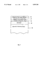
- a conventional longitudinal recording disk medium is depicted in FIG. 1 and typically comprises a non-magnetic substrate 10 having sequentially deposited thereon a plating 11, such as a plating of amorphous nickel-phosphorous (NiP), and underlayer 12, such as chromium (Cr) or a Cr-alloy, a magnetic layer 13, typically comprising a cobalt (Co)-based alloy, and a protective overcoat 14, typically containing carbon. Conventional practices also comprise bonding a lubricant topcoat (not shown) to the protective overcoat. Underlayer 12, magnetic layer 13 and protective overcoat 14 are typically deposited by sputtering techniques.
- the Co-base alloy magnetic layer deposited by conventional techniques normally comprises polycrystallites epitaxially grown on the polycrystal Cr or Cr-alloy underlayer.
- a substrate material conventionally employed in producing magnetic recording rigid disks comprises an aluminum-magnesium (Al-Mg) alloy.
- Al-Mg alloys are typically electrolessly plated with a layer of NiP at a thickness of about 15 microns to increase the hardness of the substrates, thereby providing a suitable surface for polishing to provide the requisite surface roughness or texture.
- Werner et al. U.S. Pat. No. 4,900,397, proposed the use of Radio Frequency (RF) sputter etching to remove surface deposits on a conventional NiP coating of Al-alloy substrates, followed by oxidization, to improve adhesion of a Cr underlayer.
- RF Radio Frequency
- the nickel oxide film was also said to reduce modulation by altering the crystallographic orientation of the underlayer and magnetic layer.
- Aluminum alloy substrates of magnetic recording disks exhibit an undesirable tendency to warp into potato chip shape when very thin disks are formed to satisfy increasing demands for reducing the physical size of disk drives, especially for portable computers. Such warping adversely affects control of spacing between the disk and transducer head.
- aluminum alloy substrates do not possess sufficient hardness to satisfy current disk drive shock impact requirements.
- Alternate substrate materials have been employed for magnetic recording media, such as glasses, e.g., an amorphous glass, and glass-ceramic materials which comprise a mixture of amorphous and crystalline phases. Glass-ceramic materials do not normally exhibit a crystalline surface. Glasses and glass-ceramics generally exhibit high resistance to shocks.
- the use of glass-based materials, such as glass-ceramic materials, is disclosed by Hoover et al., U.S. Pat. No. 5,273,834.
- Conventional methods for manufacturing a magnetic recording medium with a glass or glass-ceramic substrate comprise applying a seed layer between the substrate and underlayer.
- Such magnetic recording media with glass or glass-ceramic substrates are commercially available from different manufacturers with different seed layer materials to reduce the high thermal emissivity of such glass and glass-ceramic substrates, and to influence the crystallographic orientation of subsequently deposited underlayers and magnetic layers.
- Such conventional seed layer materials also include NiP which is typically sputter deposited on the surface of the glass or glass-ceramic substrate at a thickness of about 500 ⁇ .
- Conventional magnetic recording media comprising a glass or glass-ceramic substrate having NiP sputter thereon also comprise, sequentially deposited thereon, a Cr or Cr-alloy underlayer at an appropriate thickness, e.g., about 550 ⁇ , a magnetic layer such as Co-Cr-platinum (Pt)-tantalum (Ta) at an appropriate thickness, e.g., about 350 ⁇ , and a protective carbon overcoat at an appropriate thickness, e.g., about 150 ⁇ .
- Conventional Cr-alloy underlayers comprise vanadium (V) or titanium (Ti).
- Other conventional magnetic layers are CoCrTa, CoCrPtB, CoCrPt and CoNiCr.
- the seed layer, underlayer, and magnetic layer are conventionally sequentially sputter deposited on the glass or glass-ceramic substrate in an inert gas atmosphere, such as an atmosphere of pure argon.
- a conventional protective carbon overcoat is typically deposited in a mixture of argon with nitrogen, hydrogen or ethylene.
- Conventional lubricant topcoats are typically about 200 ⁇ thick.
- Magnetic films exhibiting a bicrystal cluster microstructure are expected to exhibit high coercivity, low noise and high remanent squareness.
- a magnetic recording medium comprising a glass or glass-ceramic substrate and a magnetic layer exhibiting a bicrystal cluster microstructure.
- the formation of a bicrystal cluster microstructure is induced by oxidizing the surface of a seed layer so that the underlayer subsequently deposited thereon exhibits a (200) crystallographic orientation which, in turn, induces a bicrystal cluster microstructure in a magnetic alloy layer deposited and epitaxially grown on the underlayer.
- Co-pending application Ser. No. 08/586,529, filed on Jan. 16, 1996, now U.S. Pat. No. 5,733,370 discloses a method of manufacturing a magnetic recording medium comprising a glass or glass-ceramic substrate and a magnetic layer exhibiting a bicrystal cluster microstructure.
- the disclosed method comprises sputter depositing an NiP seed layer on a glass or glass-ceramic substrate and subsequently oxidizing the deposited NiP seed layer.
- the oxidized upper seed layer surface induces the subsequently deposited underlayer to exhibit a (200) crystallographic orientation which, in turn, induces the magnetic alloy layer deposited and epitaxially grown on the underlayer to exhibit a bicrystal cluster microstructure.
- An object of the present invention is a magnetic recording medium exhibiting low noise, high coercivity, and high areal recording density.
- Another object of the present invention is a method of manufacturing a magnetic recording medium exhibiting low noise, high coercivity, and high areal recording density.
- a magnetic recording medium comprising: a substrate comprising a glass or a glass-ceramic material; a seed layer on the substrate, said seed layer having a roughened upper surface; an underlayer on the roughened upper surface of the seed layer; and a magnetic layer on the underlayer; wherein, the underlayer has an average grain size less than about 20 nm.
- a magnetic recording medium comprising: a substrate comprising a glass or glass-ceramic material; a seed layer on the substrate, said seed layer having a roughened upper surface; an underlayer on the roughened upper surface of the seed layer; and a magnetic layer on the underlayer; wherein the roughness of the seed layer surface has a peak-to-peak amplitude of about 5 ⁇ to about 100 ⁇ and a wavelength of about 5 ⁇ to about 100 ⁇ .
- a further aspect of the present invention is a method of manufacturing a magnetic recording medium, which method comprises: depositing a seed layer on a substrate comprising a glass or glass-ceramic material; roughening a surface of the seed layer; depositing an underlayer on the roughened surface of the seed layer so that the underlayer has an average grain size less than about 20 nm.
- Another aspect of the present invention is a method of manufacturing a magnetic recording medium, which method comprises: depositing seed layer on a substrate comprising a glass or glass-ceramic material; roughening a surface of the seed layer so that the surface roughness has a peak-to-peak amplitude of about 5 ⁇ to about 100 ⁇ and a wavelength of about 5 ⁇ to about 100 ⁇ ; depositing an underlayer on the roughened surface of the seed layer; and depositing a magnetic layer on the underlayer.
- FIG. 1 schematically depicts a conventional magnetic recording medium structure.
- FIG. 2 schematically depicts a magnetic recording medium structure in accordance with the present invention.
- FIG. 3A schematically illustrates the microstructure of an underlayer deposited on a smooth surface seed layer.
- FIG. 3B schematically illustrates the microstructure of an underlayer deposited on a microroughened surface seed layer in accordance with the present invention.
- FIG. 3C schematically illustrates the microstructure of a magnetic layer deposited on the underlayer illustrated in FIG. 3A.
- FIG. 3D schematically illustrates the microstructure of a magnetic layer deposited on the underlayer illustrated in FIG. 3B.
- FIG. 4 illustrates a cross sectional view of a magnetic recording medium in accordance with the present invention.
- FIG. 5 illustrates a cross sectional view of the magnetic recording medium of FIG. 3C.
- FIG. 6 illustrates magnetic clusters of a magnetic recording medium in accordance with the present invention.
- FIG. 7 illustrates the relatively larger magnetic clusters of the FIG. 5 magnetic recording medium.
- FIG. 8 is a graph illustrating the off-track capability vs. track pitch of an embodiment of the present invention.
- a bicrystal cluster microstructure is characterized by clusters of multiple magnetic crystallites, each cluster epitaxially grown on a single grain of an underlayer.
- polycrystal magnetic alloyed layers exhibit a preferred orientation.
- (11.0) planes exhibit a preference for alignment parallel to the layer plane.
- the C axes of Co-based alloy subgrains lie along two orthogonal directions. The C axes of subgrains of different clusters are randomly distributed in the film plane. See Ding et al., "Fabrication and Recording Performances of Bicrystal Disks on GaAs Substrates," Journal of The Magnetics Society of Japan, Vol. 18, Supplement, No. S1 (1994) and Ding et al, "Experimental Study on Recording and Track Edge Characteristics of Bicrystal Thin Film Media", IEEE Trans. MAGN. MAG-31, page 27, 1995.
- predominantly bicrystal cluster microstructure denotes that the magnetic layer has a microstructure which comprises greater than about 50% volume of bicrystal clusters.
- medium noise can be reduced by reducing the grain size of the underlayer, typically Cr or a Cr-alloy, and by increasing the uniformity of the grains in the underlayer, i.e., improved crystallographic morphological uniformity, aside from introducing the bicrystal cluster structure.
- the underlayer grain size and uniformity can be controlled by controlling the microroughness of the seed layer surface on which the underlayer is deposited. By controlling the microroughness of the seed layer surface to reduce the grain size and increase the uniformity of the crystallographic morphology of the chromium underlayer, the grain size and magnetic cluster size of the magnetic layer deposited on the underlayer are also reduced, thereby reducing medium noise.
- the present invention also encompasses growth of a magnetic layer having a microstructure comprising less than about 50% by volume of bicrystal clusters.
- the microroughness of a deposited seed layer is controlled to reduce the grain size of an underlayer deposited thereon and to increase the uniformity of its crystallographic morphology.
- the resulting magnetic layer sputtered deposited and epitaxial grown on the underlayer also exhibits a reduced grain and magnetic cluster sizes and significantly reduced medium noise.
- a sputter deposited seed layer such as an NiP layer
- a Cr underlayer sputter deposited thereon has an average grain size less than about 20 nm.
- a Co-base magnetic layer epitaxially grown thereon would typically exhibit a fine grain microstructure wherein the average grain size is less about 15 nm, e.g. less than about 10 nm.
- the foregoing objectives can be achieved by controlling the microroughness of a sputter deposited NiP underlayer so that the surface roughness has a peak-to-peak amplitude of about 5 ⁇ to about 100 ⁇ , e.g. about 5 ⁇ to about 50 ⁇ , and a wavelength of about 5 ⁇ to about 100 ⁇ , e.g., about 5 ⁇ to about 50 ⁇ .
- the microroughness of the seed layer is controlled to reduce the grain size in both the subsequentially sputter deposited underlayer and magnetic layer such that medium noise is significantly reduced thereby increasing areal recording density by about 40% or more.
- This objective is surprisingly achieved even though the microstructure of the magnetic layer comprises less than about 50% by volume of bicrystal clusters e.g. less than about 25% by volume of bicrystal clusters, even less than about 15% by volume of bicrystal clusters.
- the microroughness of the seed layer surface is induced and controlled by oxidation.
- a seed layer is initially sputtered deposited on a glass or glass-ceramic substrate, and the surface of the sputter deposited seed layer, e.g., NiP layer, is roughened by oxidation.
- the seed layer surface can be oxidized by heating the sputter deposited seed layer in an atmosphere containing about 1% to about 100% oxygen by volume, at a temperature above about room temperature, i.e., above about 25° C., such as up to about 300° C., to effect a desired degree of oxidation induced microroughness in the seed layer surface.
- One having ordinary skill in the art can easily determine the optimum time, duration of oxidation, temperature and amount of oxygen in the oxidizing atmosphere to induce an optimum degree of microroughness to control the grain size and crystallographic morphology of the subsequently deposited underlayer.
- a magnetic recording medium in accordance with present invention is shown in FIG. 2, and comprises a glass or glass-ceramic substrate 20 having sputter deposited thereon seed layer 21.
- the surface of seed layer is intentionally microroughened, as by oxidation.
- Underlayer 22, magnetic layer 23, and protective overcoat 24, are sequentially deposited on the seed layer.
- FIGS. 3A-3D The advantageous reduction of the grain size of a Cr underlayer and a Co-based magnetic alloy sequentially sputter deposited on an NiP seed layer with an oxidation induced microroughened upper surface is illustrated in FIGS. 3A-3D.
- FIG. 3A illustrates the grain size of a Cr layer deposited on a smooth NiP seed layer which has not been oxidized to induce surface microroughness.
- FIG. 3B illustrates the microstructure of a Cr underlayer deposited on an oxidation induced microroughened NiP seed layer in accordance with the present invention.
- FIG. 3C illustrates the microstructure of a Co-base magnetic alloy sputter deposited on the Cr underlayer of FIG. 3A deposited on a smooth NiP seed layer.
- FIG. 3A illustrates the grain size of a Cr layer deposited on a smooth NiP seed layer which has not been oxidized to induce surface microroughness.
- FIG. 3B illustrates the microstructure of a Cr underlayer deposited on an
- FIG. 3D illustrates the microstructure of a Co-base magnetic alloy sputter deposited on the Cr underlayer shown in FIG. 3B deposited on an oxidation induced microroughened NiP seed layer in accordance with the present invention. It should be apparent from FIGS. 3A-3D that the oxidation induced microroughened seed layer surface advantageously reduces the grain size of the subsequently sequentially deposited underlayer and magnetic layer.
- a magnetic recording medium produced in accordance with the present invention comprises glass-ceramic substrate 40 with an oxidized NiP seed layer 41 thereon.
- the subsequently deposited Cr underlayer 42 exhibits a relatively fine grain size which in turn, induces the subsequently deposited magnetic cobalt alloy magnetic layer 43 to exhibit a relatively fine grain size and relatively small magnetic clusters.
- the NiP sputter deposited seed layer 51 formed on glass-ceramic substrate 40 is not oxidized, i.e. it has a relatively smooth upper surface.
- the subsequently sputter deposited Cr underlayer 52 consequently, exhibits a grain size which is relatively larger, and a crystallographic morphology less uniform, than those of Cr layer 42 of FIG. 4 which was sputter deposited on a microroughened seed layer surface.
- FIGS. 4 and 5 further illustrates that for a relatively large Cr underlayer (52) grain size, several Co-alloy grains grow on a single Cr grain to form a magnetic cluster larger than those formed in magnetic layer 43 on a single Cr grain of Cr underlayer (42) in accordance with the present invention illustrated in FIG. 4.
- the relatively smaller grain size of Cr underlayer 42 of FIG. 4 induces the growth very few Co-alloy grains on a single Cr grain and hence, smaller magnetic clusters are formed vis-a-vis magnetic layer 53 of FIG. 5.
- the origin of media noise stems from the irregular shape of transitions due to finite magnetic cluster size. See Tu Chen, "The Micromagnetic Properties of High-Coercivity Metallic Thin Films and Their Effects on the Limit of Packing Density in Digital Recording," IEEE Trans. Magn. Vol. MAG-17, pp. 1181-1191, 1981.
- the magnetic cluster is related to the grain size of the Cr underlayer. See J. J. Miles et al., IEEE Trans. Magn., Vol. MAG-31, p. 1013, 1995. In this case, more Co alloy subgrains are grown on a Cr underlayer grain, which results in a larger magnetic cluster through strong inner intergranular exchange coupling.
- the outer intergranular exchange coupling is relatively weak due to Cr segregation at boundaries between clusters.
- the magnetic cluster is the smallest switching volume during a magnetization reversal process. Therefore, transition follows the boundaries of magnetic clusters. A smaller magnetic cluster has less variance of transition, which results in low media noise; whereas, a larger magnetic cluster has more variance of transition which leads to high media noise.
- J. J. Miles et al. IEEE Trans. Magn., Vol. MAG-31, p. 1013, 1995, J. K. Chang et al., "Evolution of Bicrystal Media” TMR conference, Santa Clara, 1996.
- FIG. 6 illustrates the microstructure of a magnetic layer formed in accordance with the present invention having magnetic clusters 60 which are smaller than magnetic clusters 70 formed on an underlayer deposited on a seed layer with a relatively smooth upper surface, as shown in FIG. 7. It is apparent from a comparison of FIGS. 6 and 7, that the magnetic orientation transition shape 61 across the magnetic cluster 60 in accordance with the present invention illustrated in FIG. 6 has greater regularity and uniformity than the transition shape 71 across the relatively larger magnetic clusters 70 illustrated in FIG. 7.
- a glass-ceramic substrate was preheated to a temperature of about 250° C., and an NiP seed layer was sputtered deposited thereon at a pressure of about 10 mTorr. After sputter deposition, the NiP seed layer was exposed to an atmosphere containing argon and about 20 volume percent oxygen at a temperature in excess of 100° C. to induce a desired surface microroughness. Subsequently, a Cr underlayer, CoCrPtTa magnetic layer and protective carbon overcoat were sequentially sputtered deposited at a working pressure of about 10 mTorr and a temperature of about 150° C. to about 250° C.
- the resulting magnetic recording medium representative of the present invention is identified as Sample B.
- a magnetic recording medium identified as Sample A was fabricated in an identical manner as Sample B except that the sputtered deposited NiP seed layer was not oxidized to induce surface microroughness.
- the grain size and microroughness were determined employing a Philip 430 electron microscope operating at 300 kV.
- High resolution transmission electron microscope (HRTEM) images of the interface between the Cr and NiP layers confirmed the formation of seed layer surface microroughness upon oxidation in Sample B; however, no such microroughness was apparent from the HRTEM image of Sample A.
- HRTEM images also revealed that the larger Cr grains of Sample A contained more Co-alloy grains per Cr grain than the smaller Cr grains of Sample B.
- the grain size of the Cr underlayer of Sample A was about 20 nm to about 40 nm, while the grain size of the CoCrPtTa magnetic layer ranged from about 5 nm to about 20 nm.
- the Cr grain size ranged from about 5 n to about 20 nm, while the grain size the CoCrPtTa magnetic layer ranged from about 3 nm to about 10 nm.
- the magnetic transition shape was observed by employing a magnetic force microscope to form images of written magnetization bits patterned at 100 Kfci on Samples A and B. It was observed that the medium with the smooth layer (Sample A) has a magnetic orientation transition shape with significantly greater irregularity than that of the magnetic recording medium with the rough seed layer (Sample B).
- the magnetic properties of the Samples A and B were measured using a vibrating sample magnetometer.
- the recording performance of the Samples were evaluated on a Guzik 1701 spinstand through a Guzik 1601 read-write analyzer.
- An inductive head with a write track width of 2.9 ⁇ m and gap length of 0.5 ⁇ m were employed in the writing process.
- a magnetoresistive head with a read track width of 2.4 ⁇ m and shield spacing of 0.35 ⁇ m was used.
- the head medium spacing was 1.8 ⁇ in.
- the medium transition noise was measured by integrating the power spectrum over a bandwidth of 70 MHz and subtracting off the DC and electronics noise.
- the magnetic properties and recording results at 100 Kfci for Samples A and B are listed in Table II.
- SNR denotes the signal-to-noise ratio
- OW denotes overwrite
- PW50 denotes the pulse width at half maximum of the signal output. It is apparent from Table II that Sample B fabricated in accordance with the present invention exhibits an SNR of greater than 6 dB, and superior OW, than Sample A prepared without inducing microroughness in the seed layer surface.
- the track density was determined by off-track-capability (OTC) measurements.
- FIG. 8 shows the OTC capability vs. track pitch for Samples A and B.
- the bit error rate for the OTC test is 10 -8 .
- the minimum track pitch is 134 ⁇ in for Sample A and 122 ⁇ in for Sample B.
- Table III set forth below, summarizes the areal density for both Sample A and B. It should be apparent that the areal density for Sample B is about 40% higher than that for Sample A.
- the present invention comprises a magnetic recording medium having a significantly improved SNR by virtue controlling the surface roughness of a seed layer, as by controlling the oxidation of its surface subsequent to sputter deposition on a glass or glass-ceramic substrate.
- the subsequently deposited Cr or Cr-alloy underlayer exhibits a fine grain size and uniform crystallographic morphology.
- the magnetic recording medium of the present invention advantageously exhibit significantly reduced medium noise vis-a-vis magnetic recording media with glass or glass-ceramic substrates produced without controlling the microroughness of the seed layer deposited on the substrate.
- the magnetic recording media of the present invention also exhibit a high coercivity even at a low Mrt and, hence, are particularly suitable for high areal density magnetic recording.
- the substrates employed in the present invention can advantageously comprise any of various glass or glass-ceramic materials, such as those previously been employed as substrates for magnetic recording media.
- Glass-ceramic materials are typically formed by a heat treatment of the surface to form a thin crystallized layer of ceramic thereon.
- suitable conventional glass-ceramic material are referred to as "Ohara glass.”
- the underlayer employed in the present invention can comprise any of various materials conventionally employed as an underlayer in the production of magnetic recording media, such as Cr, CrV, CrTi or CrMo. It has been found that an underlayer thickness of about 100 ⁇ to about 2000 ⁇ , such as about 550 ⁇ , is suitable.
- the magnetic layer of the present invention can comprise any magnetic alloy conventionally employed in the production of magnetic recording media.
- Such alloys include, but are not limited to, Co-based alloys such as CoCr, CoCrTa, CoNiCr, CoCrPtTa, CoCrPt, CoNiPt, CoNiCrPt and CoCrPtB.
- the thickness of the magnetic layer is consistent with the thickness of magnetic layers of conventional magnetic recording media.
- a protective overcoat can be deposited on the magnetic layer by any conventional means, such as sputtering.
- Protective overcoats can comprise zirconium oxide (ZrO 2 ), carbon, including hydrogenated carbon, silicon carbide (SiC), or a carbon nitride (CN).
- the protective overcoat is provided in a thickness suitable to protect the underlying layers.
- An overcoat having a thickness of about 50 ⁇ to about 300 ⁇ , such as about 100 ⁇ to 200 ⁇ has been found suitable.
- a layer of a lubricant can be applied on and bonded to the overcoat.
- the lubricant topcoat can be provided in any suitable thickness.
- the magnetic recording media produced in accordance with the present invention typically exhibit a coercivity greater than 2000 Oersteds and an Mrt of about 0.4 to about 3.0 memu/cm 2 .
- the apparatus employed in the present invention can be any of those sputtering apparatus conventionally employed in the production of magnetic recording medium.
- the present invention is not limited to the specific examples disclosed herein, the particular deposition techniques or the particular materials previously exemplified or mentioned.
- the seed layer can be deposited by any of various electrical plating techniques as an alternative to sputter deposition.
- the magnetic recording media of the present invention can comprise any of various types of glass, glass-ceramic, carbon and ceramic substrates, and various types of magnetic alloy layers, including various Co-based alloy magnetic layers.
- the underlayer of the present magnetic recording media is not limited to Cr, but can comprise various other materials, including metals exhibiting a cubic polycrystal structure.
- the magnetic recording media of the present invention enjoy utility in various applications, particularly applications wherein high density is required, such as a magnetic rigid disk medium for longitudinal recording.
Abstract
Description
              TABLE I
______________________________________
                 Temp.     Temp.
                 (Cr-      (Magnetic
Sample
      Pressure   Underlayer)
                           Layer)   NiP
______________________________________
A     10 mTorr   250° C.
                           200° C.
                                    No Oxidation
B     10 mTorr   250° C.
                           200° C.
                                    Oxidation
______________________________________
              TABLE II
______________________________________
      Hc      Mrt                 PW50  OW   SNR
Sample
      (Oe)    (emu/cm.sup.2)
                       S*   S     (ns)  (db) (db)
______________________________________
A     2330    0.98     0.83 0.78  26.1  37.3 14.5
B     2109    0.96     0.83 0.81  25.7  42.3 20.7
______________________________________
              TABLE III
______________________________________
                                       Areal
                        Min. Track     density
Sample  kfci     KBPI   pitch (μin)
                                  TPI  (Gb/in.sup.2)
______________________________________
A       100      88.9   134.0     7500 0.67
B       150      133.3  121.6     8200 1.09
______________________________________
Claims (44)
Priority Applications (1)
| Application Number | Priority Date | Filing Date | Title |
|---|---|---|---|
| US08/735,443 US5879783A (en) | 1996-08-05 | 1997-01-02 | Low noise magnetic recording medium and method of manufacturing |
Applications Claiming Priority (2)
| Application Number | Priority Date | Filing Date | Title |
|---|---|---|---|
| US2322896P | 1996-08-05 | 1996-08-05 | |
| US08/735,443 US5879783A (en) | 1996-08-05 | 1997-01-02 | Low noise magnetic recording medium and method of manufacturing |
Publications (1)
| Publication Number | Publication Date |
|---|---|
| US5879783A true US5879783A (en) | 1999-03-09 |
Family
ID=26696879
Family Applications (1)
| Application Number | Title | Priority Date | Filing Date |
|---|---|---|---|
| US08/735,443 Expired - Lifetime US5879783A (en) | 1996-08-05 | 1997-01-02 | Low noise magnetic recording medium and method of manufacturing |
Country Status (1)
| Country | Link |
|---|---|
| US (1) | US5879783A (en) |
Cited By (27)
| Publication number | Priority date | Publication date | Assignee | Title |
|---|---|---|---|---|
| US6081394A (en) * | 1997-01-16 | 2000-06-27 | Nec Corporation | Recorded magnetization state measuring method and device |
| US6110582A (en) * | 1997-09-08 | 2000-08-29 | Seagate Technology, Inc. | Substantially two dimensional isotropic magnetic recording medium comprising a NiAl underlayer |
| US6117570A (en) * | 1998-03-19 | 2000-09-12 | Seagate Technology, Inc. | Thin film medium with surface-oxidized NiAl seed layer |
| US6132863A (en) * | 1997-12-12 | 2000-10-17 | Seagate Technology Llc | Magnetic recording medium with grain size control layer |
| US6139951A (en) * | 1997-12-12 | 2000-10-31 | Seagate Technology Llc | Magnetic recording medium with low temperature seedlayer for high signal-to-noise ratio |
| US6162526A (en) * | 1996-08-30 | 2000-12-19 | Hoya Corporation | Magnetic recording medium having a crystalized glass substrate |
| US6242085B1 (en) * | 1997-09-17 | 2001-06-05 | Matsushita Electric Industrial Co., Ltd. | Magnetic recording medium and method for producing the same |
| US20020044393A1 (en) * | 2001-03-15 | 2002-04-18 | Seigler Michael A. | Multilayer permanent magnet films |
| US20030017364A1 (en) * | 2001-06-29 | 2003-01-23 | Kabushiki Kaisha Toshiba | Magnetic recording medium, magnetic recording apparatus and magnetic recording method |
| US6511855B2 (en) * | 1998-01-06 | 2003-01-28 | Hewlett-Packard Company | Method of forming ferromagnetic tunnel junctions with enhanced magneto-resistance |
| US6560077B2 (en) * | 2000-01-10 | 2003-05-06 | The University Of Alabama | CPP spin-valve device |
| US6579613B1 (en) * | 1999-10-14 | 2003-06-17 | Fuji Electric Co., Ltd. | Recording medium with limited using period |
| US6593009B2 (en) | 2001-03-02 | 2003-07-15 | Hitachi Global Storage Technologies Netherlands N.V. | Magnetic thin film media with a pre-seed layer of CrTi |
| US6620531B1 (en) | 1999-12-20 | 2003-09-16 | Seagate Technology Llc | Magnetic recording media with oxidized seedlayer for reduced grain size and reduced grain size distribution |
| US6620532B2 (en) * | 2000-01-21 | 2003-09-16 | Tdk Corporation | Magnetic recording medium and magnetic write/read method |
| US20030224211A1 (en) * | 2002-05-29 | 2003-12-04 | Xiaoping Bian | Preseed layer for a magnetic recording disk |
| US20040001367A1 (en) * | 2002-06-28 | 2004-01-01 | Seagate Technology Llc | Increased packing density in self-organized magnetic tray |
| US6677051B1 (en) * | 1999-12-10 | 2004-01-13 | Fujitsu Limited | Magnetic recording medium with dual magnetic layers having specific composition requirements and a magnetic storage apparatus |
| US20040009372A1 (en) * | 2002-03-13 | 2004-01-15 | Toyoji Ataka | Magnetic recording medium and manufacturing method thereof |
| US6740383B2 (en) * | 1998-05-27 | 2004-05-25 | Fujitsu Limited | Magnetic recording medium possessing a ratio of Hc(perpendicular) to Hc(horizontal) that is not more than 0.22 and magnetic recording disk device |
| US20040170869A1 (en) * | 2002-10-14 | 2004-09-02 | Sung-Chul Shin | High density magnetic recording medium having uniform local coercivity distribution and grain size distribution and fine grains and manufacturing method thereof |
| US6849164B2 (en) | 2001-05-11 | 2005-02-01 | Fuji Electric Co., Ltd. | Magnetic recording medium and method of manufacturing the same |
| US6852430B2 (en) | 2001-03-02 | 2005-02-08 | Hitachi Global Storage Technologies Netherlands, B.V. | Magnetic thin film media with a pre-seed layer of CrTi |
| US6858331B1 (en) | 2003-08-29 | 2005-02-22 | Hitachi Global Storage Technologies Netherlands, B.V. | Magnetic thin film media with a bi-layer structure of CrTi/Nip |
| US20050164038A1 (en) * | 2003-09-16 | 2005-07-28 | Seagate Technology Llc | Highly oriented longitudinal magnetic media on direct textured glass substrates |
| US20050190478A1 (en) * | 2004-03-01 | 2005-09-01 | Hsiao Wenchien D. | Longitudinal magnetic recording using magnetic media with a soft underlayer |
| US20060286411A1 (en) * | 1998-08-28 | 2006-12-21 | Nippon Telegraph And Telephone Corporation And The Centre National De La Recherche Scientifique | Magneto-optical recording medium, manufacturing method thereof and magneto-optical data recording and playback device |
Citations (4)
| Publication number | Priority date | Publication date | Assignee | Title |
|---|---|---|---|---|
| US4900397A (en) * | 1987-08-08 | 1990-02-13 | Basf Aktiengesellschaft | Production of magnetic recording media |
| US4900387A (en) * | 1988-02-24 | 1990-02-13 | The Boeing Company | Method of bonding via electrorheological adhesives |
| US5273834A (en) * | 1993-01-25 | 1993-12-28 | Corning Incorporated | Discs for memory storage devices |
| US5302434A (en) * | 1992-08-07 | 1994-04-12 | International Business Machines Corporation | Magnetic recording disk for contact recording |
-
1997
- 1997-01-02 US US08/735,443 patent/US5879783A/en not_active Expired - Lifetime
Patent Citations (4)
| Publication number | Priority date | Publication date | Assignee | Title |
|---|---|---|---|---|
| US4900397A (en) * | 1987-08-08 | 1990-02-13 | Basf Aktiengesellschaft | Production of magnetic recording media |
| US4900387A (en) * | 1988-02-24 | 1990-02-13 | The Boeing Company | Method of bonding via electrorheological adhesives |
| US5302434A (en) * | 1992-08-07 | 1994-04-12 | International Business Machines Corporation | Magnetic recording disk for contact recording |
| US5273834A (en) * | 1993-01-25 | 1993-12-28 | Corning Incorporated | Discs for memory storage devices |
Non-Patent Citations (32)
| Title |
|---|
| Chang, Jack J.K., Evolution of Bicrystal Media Development, TMR Conference, Santa Clara, 1996. * |
| Chen, Qixu, et al, "Thin Film Media With and Without Bicrystal Cluster Structure on Glass Ceramic Substrates," Intermag Conference GC-6, Seattle, 1996 (3 pages.). |
| Chen, Qixu, et al, Thin Film Media With and Without Bicrystal Cluster Structure on Glass Ceramic Substrates, Intermag Conference GC 6, Seattle, 1996 (3 pages.). * |
| Chen, Tu, "The Micromagnetic Properties of High-Coercivity Metallic Thin Films and Their Effects on the Limit of Packing Density in Digital Recording," IEEE Transactions on Magnetics, Mar. 1981, pp. 1181-1191. |
| Chen, Tu, The Micromagnetic Properties of High Coercivity Metallic Thin Films and Their Effects on the Limit of Packing Density in Digital Recording, IEEE Transactions on Magnetics, Mar. 1981, pp. 1181 1191. * |
| D.E. Long Win et al. "Epitaxy and Crystallorganic Texture . . . " Material Research Society Symposium, vol. 343, Aug. 1994. |
| D.E. Long Win et al. Epitaxy and Crystallorganic Texture . . . Material Research Society Symposium, vol. 343, Aug. 1994. * |
| Ding, Juren, et al, "Experimental Study on Recording and Track Edge Characteristics of Bicrystal Thin Film Media," IEEE Transactions on Magnetics, MAG-31, 1995, p. 27. |
| Ding, Juren, et al, "Microstructure and Recording Properties of Bicrystal Disks With GaAs Substrates," IEEE Transactions on Magnetics, Nov. 1994, pp. 3978-3980. |
| Ding, Juren, et al, Experimental Study on Recording and Track Edge Characteristics of Bicrystal Thin Film Media, IEEE Transactions on Magnetics, MAG 31, 1995, p. 27. * |
| Ding, Juren, et al, Fabrication and Recording Performances of Bicrystal Disks on GaAs Substrates, Journal of the Magnetics Society of Japan, vol. 18, Supplement No. S1, 1994. * |
| Ding, Juren, et al, Microstructure and Recording Properties of Bicrystal Disks With GaAs Substrates, IEEE Transactions on Magnetics, Nov. 1994, pp. 3978 3980. * |
| Futamoto, Masaki, et al, "Magnetic and Recording Characteristics of Bicrystalline Longitudinal Recording Medium Formed on an MgO Single Crystal Disk Substrate," IEEE Transactions on Magnetics, Nov. 1994, pp. 3975-3977. |
| Futamoto, Masaki, et al, Magnetic and Recording Characteristics of Bicrystalline Longitudinal Recording Medium Formed on an MgO Single Crystal Disk Substrate, IEEE Transactions on Magnetics, Nov. 1994, pp. 3975 3977. * |
| Hosoe, Y., Bicrystal Cluster Structure and Magnetic Properties of CoCrTa/Cr Thin Film Media, IEEE, Sep. 1995. * |
| Laughlin, David E., et al, "Epitaxy and Crystallographic Texture of Thin Films for Magnetic Recording," Material Research Society Symposium, vol. 343, 1994, pp. 327-337. |
| Laughlin, David E., et al, Epitaxy and Crystallographic Texture of Thin Films for Magnetic Recording, Material Research Society Symposium, vol. 343, 1994, pp. 327 337. * |
| Miles, Jim, J., et al, "The Effect of Cluster Size of Thin Film Media Noise," IEEE Transactions on Magnetics, Mar. 1995, pp. 1013-1023. |
| Miles, Jim, J., et al, The Effect of Cluster Size of Thin Film Media Noise, IEEE Transactions on Magnetics, Mar. 1995, pp. 1013 1023. * |
| Min, Tai, et al, "Bicrystal Advanced Thin-film Media for High Density Recording," Journal of Applied Physics, May 15, 1994, pp. 6129-6131. |
| Min, Tai, et al, Bicrystal Advanced Thin film Media for High Density Recording, Journal of Applied Physics, May 15, 1994, pp. 6129 6131. * |
| Mirzamaani, M., et al, "Magnetic Properties of CoPtCr Thin Films with <1120> Crystal Orientation," Journal of Applied Physics, Apr. 15, 1991, pp. 5169-5171. |
| Mirzamaani, M., et al, Magnetic Properties of CoPtCr Thin Films with 1120 Crystal Orientation, Journal of Applied Physics, Apr. 15, 1991, pp. 5169 5171. * |
| Nolan, T. P., et al, "Effect of Microstructural Features on Media Noise in Longitudinal Recording Media," Journal of Applied Physics, May 15, 1993, pp. 5566-5568. |
| Nolan, T. P., et al, Effect of Microstructural Features on Media Noise in Longitudinal Recording Media, Journal of Applied Physics, May 15, 1993, pp. 5566 5568. * |
| Peng, Qingzhi, et al, Micromagnetic and Experimental Studies of CoPtCr Bicrystal Thin Film Media, IEEE, Sep. 1995. * |
| Wong, B.Y., "Investigation of CoNiCr Thin Films Deposited on 100! and 110! Cr Single Crystals," IEEE Transactions on Magnetics, Nov. 1991, pp. 4733-4735. |
| Wong, B.Y., Investigation of CoNiCr Thin Films Deposited on 100 and 110 Cr Single Crystals, IEEE Transactions on Magnetics, Nov. 1991, pp. 4733 4735. * |
| Yahisa, Y., et al, "Electron Spectroscopic Imaging Analysis of Compositional Inhomogeneity in CoCrTa Longitudinal Thin Film Media," IEEE Transactions on Magnetics, Nov. 1995, pp. 2836-2838. |
| Yahisa, Y., et al, Electron Spectroscopic Imaging Analysis of Compositional Inhomogeneity in CoCrTa Longitudinal Thin Film Media, IEEE Transactions on Magnetics, Nov. 1995, pp. 2836 2838. * |
| Ye, Xiao Guang, et al, Modeling of Thin film Media With Advanced Microstructure for Ultrahigh Density Recording, Journal of Applied Physics, May 15, 1994, pp. 6135 6137. * |
| Ye, Xiao-Guang, et al, "Modeling of Thin-film Media With Advanced Microstructure for Ultrahigh Density Recording," Journal of Applied Physics, May 15, 1994, pp. 6135-6137. |
Cited By (42)
| Publication number | Priority date | Publication date | Assignee | Title |
|---|---|---|---|---|
| US6379775B1 (en) | 1996-08-30 | 2002-04-30 | Hoya Corporation | Magnetic recording medium and method of manufacturing the same |
| US6162526A (en) * | 1996-08-30 | 2000-12-19 | Hoya Corporation | Magnetic recording medium having a crystalized glass substrate |
| US6081394A (en) * | 1997-01-16 | 2000-06-27 | Nec Corporation | Recorded magnetization state measuring method and device |
| US6110582A (en) * | 1997-09-08 | 2000-08-29 | Seagate Technology, Inc. | Substantially two dimensional isotropic magnetic recording medium comprising a NiAl underlayer |
| US6242085B1 (en) * | 1997-09-17 | 2001-06-05 | Matsushita Electric Industrial Co., Ltd. | Magnetic recording medium and method for producing the same |
| US6132863A (en) * | 1997-12-12 | 2000-10-17 | Seagate Technology Llc | Magnetic recording medium with grain size control layer |
| US6139951A (en) * | 1997-12-12 | 2000-10-31 | Seagate Technology Llc | Magnetic recording medium with low temperature seedlayer for high signal-to-noise ratio |
| US6511855B2 (en) * | 1998-01-06 | 2003-01-28 | Hewlett-Packard Company | Method of forming ferromagnetic tunnel junctions with enhanced magneto-resistance |
| US6117570A (en) * | 1998-03-19 | 2000-09-12 | Seagate Technology, Inc. | Thin film medium with surface-oxidized NiAl seed layer |
| US6740383B2 (en) * | 1998-05-27 | 2004-05-25 | Fujitsu Limited | Magnetic recording medium possessing a ratio of Hc(perpendicular) to Hc(horizontal) that is not more than 0.22 and magnetic recording disk device |
| US20060286411A1 (en) * | 1998-08-28 | 2006-12-21 | Nippon Telegraph And Telephone Corporation And The Centre National De La Recherche Scientifique | Magneto-optical recording medium, manufacturing method thereof and magneto-optical data recording and playback device |
| US7368146B2 (en) * | 1998-08-28 | 2008-05-06 | Nippon Telegraph And Telephone Corporation | Magneto-optical recording medium, manufacturing method thereof and magneto-optical data recording and playback device |
| US6579613B1 (en) * | 1999-10-14 | 2003-06-17 | Fuji Electric Co., Ltd. | Recording medium with limited using period |
| US6677051B1 (en) * | 1999-12-10 | 2004-01-13 | Fujitsu Limited | Magnetic recording medium with dual magnetic layers having specific composition requirements and a magnetic storage apparatus |
| US6620531B1 (en) | 1999-12-20 | 2003-09-16 | Seagate Technology Llc | Magnetic recording media with oxidized seedlayer for reduced grain size and reduced grain size distribution |
| US6560077B2 (en) * | 2000-01-10 | 2003-05-06 | The University Of Alabama | CPP spin-valve device |
| US6620532B2 (en) * | 2000-01-21 | 2003-09-16 | Tdk Corporation | Magnetic recording medium and magnetic write/read method |
| US6593009B2 (en) | 2001-03-02 | 2003-07-15 | Hitachi Global Storage Technologies Netherlands N.V. | Magnetic thin film media with a pre-seed layer of CrTi |
| US20050031909A1 (en) * | 2001-03-02 | 2005-02-10 | Xiaoping Bian | Magnetic thin film media with a pre-seed layer of CrTi |
| US6852430B2 (en) | 2001-03-02 | 2005-02-08 | Hitachi Global Storage Technologies Netherlands, B.V. | Magnetic thin film media with a pre-seed layer of CrTi |
| US7050274B2 (en) * | 2001-03-15 | 2006-05-23 | Seagate Technology Llc | Multilayer permanent magnet films |
| US20020044393A1 (en) * | 2001-03-15 | 2002-04-18 | Seigler Michael A. | Multilayer permanent magnet films |
| US6849164B2 (en) | 2001-05-11 | 2005-02-01 | Fuji Electric Co., Ltd. | Magnetic recording medium and method of manufacturing the same |
| US6881495B2 (en) * | 2001-06-29 | 2005-04-19 | Kabushiki Kaisha Toshiba | Magnetic recording medium including functional and recording layers orthogonally exchange coupled |
| US20030017364A1 (en) * | 2001-06-29 | 2003-01-23 | Kabushiki Kaisha Toshiba | Magnetic recording medium, magnetic recording apparatus and magnetic recording method |
| US7330335B2 (en) | 2001-06-29 | 2008-02-12 | Kabushiki Kaisha Toshiba | Magnetic recording medium, magnetic recording apparatus and magnetic recording method |
| US20080096050A1 (en) * | 2001-06-29 | 2008-04-24 | Kabushiki Kaisha Toshiba | Magnetic recording medium, magnetic recording apparatus and magnetic recording method |
| US20050041335A1 (en) * | 2001-06-29 | 2005-02-24 | Kabushiki Kaisha Toshiba | Magnetic recording medium, magnetic recording apparatus and magnetic recording method |
| US7014882B2 (en) * | 2002-03-13 | 2006-03-21 | Fuji Electric Co., Ltd. | Magnetic recording medium and manufacturing method thereof |
| US20060115686A1 (en) * | 2002-03-13 | 2006-06-01 | Fuji Electric Co., Ltd. | Magnetic recording medium and manufacturing method thereof |
| US20040009372A1 (en) * | 2002-03-13 | 2004-01-15 | Toyoji Ataka | Magnetic recording medium and manufacturing method thereof |
| US6677052B2 (en) * | 2002-05-29 | 2004-01-13 | Hitachi Global Storage Technologies | Preseed layer for a magnetic recording disk |
| US20030224211A1 (en) * | 2002-05-29 | 2003-12-04 | Xiaoping Bian | Preseed layer for a magnetic recording disk |
| US6838195B2 (en) | 2002-06-28 | 2005-01-04 | Seagate Technology Llc | Increased packing density in self-organized magnetic tray |
| US20040001367A1 (en) * | 2002-06-28 | 2004-01-01 | Seagate Technology Llc | Increased packing density in self-organized magnetic tray |
| US7294419B2 (en) * | 2002-10-14 | 2007-11-13 | Korea Advanced Institute Of Science And Technology | High density magnetic recording medium having uniform local coercivity distribution and grain size distribution and fine grains and manufacturing method thereof |
| US20040170869A1 (en) * | 2002-10-14 | 2004-09-02 | Sung-Chul Shin | High density magnetic recording medium having uniform local coercivity distribution and grain size distribution and fine grains and manufacturing method thereof |
| US6858331B1 (en) | 2003-08-29 | 2005-02-22 | Hitachi Global Storage Technologies Netherlands, B.V. | Magnetic thin film media with a bi-layer structure of CrTi/Nip |
| US20050048328A1 (en) * | 2003-08-29 | 2005-03-03 | Xiaoping Bian | Magnetic thin film media with a bi-layer structure of crti/nip |
| US20050164038A1 (en) * | 2003-09-16 | 2005-07-28 | Seagate Technology Llc | Highly oriented longitudinal magnetic media on direct textured glass substrates |
| US20050190478A1 (en) * | 2004-03-01 | 2005-09-01 | Hsiao Wenchien D. | Longitudinal magnetic recording using magnetic media with a soft underlayer |
| US7092209B2 (en) * | 2004-03-01 | 2006-08-15 | Hitachi Global Storage Technologies Netherlands B.V. | Longitudinal magnetic recording using magnetic media with a soft underlayer |
Similar Documents
| Publication | Publication Date | Title |
|---|---|---|
| US5879783A (en) | Low noise magnetic recording medium and method of manufacturing | |
| US6562489B2 (en) | Magnetic recording medium and magnetic storage apparatus | |
| US7851014B2 (en) | Tilted recording media with L10 magnetic layer | |
| US6156404A (en) | Method of making high performance, low noise isotropic magnetic media including a chromium underlayer | |
| US6586116B1 (en) | Nonmetallic thin film magnetic recording disk with pre-seed layer | |
| US6010795A (en) | Magnetic recording medium comprising a nickel aluminum or iron aluminum underlayer and chromium containing intermediate layer each having (200) dominant crystalographic orientation | |
| JP2002056522A (en) | Magnetic recording medium and its manufacturing method | |
| US5866227A (en) | Magnetic recording medium with partially oxidized seed layer | |
| US6942933B2 (en) | Magnetic recording medium, production process thereof, and magnetic recording and reproducing apparatus | |
| US6221481B1 (en) | High Cr, low saturation magnetization intermediate magnetic layer for high coercivity and low medium noise | |
| US6403241B1 (en) | CoCrPtB medium with a 1010 crystallographic orientation | |
| JP3298893B2 (en) | Bicrystalline cluster magnetic recording media | |
| US6110582A (en) | Substantially two dimensional isotropic magnetic recording medium comprising a NiAl underlayer | |
| US6150016A (en) | High coercivity magnetic recording medium comprising a thin CoCrTa intermediate layer | |
| JP2005004945A (en) | Perpendicular magnetic recording medium and its manufacturing method | |
| JP2001344740A (en) | Magnetic recording medium and magnetic storage device | |
| US6759149B1 (en) | Laminated medium with antiferromagnetic stabilization layers | |
| US7521136B1 (en) | Coupling enhancement for medium with anti-ferromagnetic coupling | |
| US6156422A (en) | High density magnetic recording medium with high Hr and low Mrt | |
| US6146754A (en) | Substantially isotropic magnetic recording medium comprising a seedlayer | |
| US6139981A (en) | Magnetic thin film medium with adhesion enhancement layer | |
| US6936353B1 (en) | Tilted recording medium design with (101-2) orientation | |
| US6242086B1 (en) | High coercivity, low noise magnetic recording medium comprising an intermediate cocrtaox layer | |
| JP3983813B2 (en) | Magnetic recording medium comprising a nickel-aluminum or iron-aluminum underlayer | |
| JPH11219511A (en) | Magnetic recording medium and magnetic recording device |
Legal Events
| Date | Code | Title | Description |
|---|---|---|---|
| AS | Assignment |
Owner name: SEAGATE TECHNOLOGY, CALIFORNIA Free format text: ASSIGNMENT OF ASSIGNORS INTEREST;ASSIGNORS:CHANG, JYH-KAU;CHEN, QIXU;CHEN, GA-LANE;REEL/FRAME:008353/0920 Effective date: 19961231 |
|
| STCF | Information on status: patent grant |
Free format text: PATENTED CASE |
|
| AS | Assignment |
Owner name: SEAGATE TECHNOLOGY LLC, CALIFORNIA Free format text: ASSIGNMENT OF ASSIGNORS INTEREST;ASSIGNOR:SEAGATE TECHNOLOGY, INC.;REEL/FRAME:011077/0319 Effective date: 20000728 |
|
| AS | Assignment |
Owner name: THE CHASE MANHATTAN BANK, AS COLLATERAL AGENT, NEW Free format text: SECURITY AGREEMENT;ASSIGNOR:SEAGATE TECHNOLOGY LLC;REEL/FRAME:011461/0001 Effective date: 20001122 |
|
| FPAY | Fee payment |
Year of fee payment: 4 |
|
| AS | Assignment |
Owner name: JPMORGAN CHASE BANK, AS COLLATERAL AGENT, NEW YORK Free format text: SECURITY AGREEMENT;ASSIGNOR:SEAGATE TECHNOLOGY LLC;REEL/FRAME:013177/0001 Effective date: 20020513 Owner name: JPMORGAN CHASE BANK, AS COLLATERAL AGENT,NEW YORK Free format text: SECURITY AGREEMENT;ASSIGNOR:SEAGATE TECHNOLOGY LLC;REEL/FRAME:013177/0001 Effective date: 20020513 |
|
| AS | Assignment |
Owner name: SEAGATE TECHNOLOGY LLC, CALIFORNIA Free format text: RELEASE OF SECURITY INTERESTS IN PATENT RIGHTS;ASSIGNOR:JPMORGAN CHASE BANK, N.A. (FORMERLY KNOWN AS THE CHASE MANHATTAN BANK AND JPMORGAN CHASE BANK), AS ADMINISTRATIVE AGENT;REEL/FRAME:016945/0712 Effective date: 20051130 |
|
| FPAY | Fee payment |
Year of fee payment: 8 |
|
| AS | Assignment |
Owner name: JPMORGAN CHASE BANK, N.A., AS ADMINISTRATIVE AGENT Free format text: SECURITY AGREEMENT;ASSIGNORS:MAXTOR CORPORATION;SEAGATE TECHNOLOGY LLC;SEAGATE TECHNOLOGY INTERNATIONAL;REEL/FRAME:022757/0017 Effective date: 20090507 Owner name: WELLS FARGO BANK, NATIONAL ASSOCIATION, AS COLLATE Free format text: SECURITY AGREEMENT;ASSIGNORS:MAXTOR CORPORATION;SEAGATE TECHNOLOGY LLC;SEAGATE TECHNOLOGY INTERNATIONAL;REEL/FRAME:022757/0017 Effective date: 20090507 |
|
| FPAY | Fee payment |
Year of fee payment: 12 |
|
| AS | Assignment |
Owner name: MAXTOR CORPORATION, CALIFORNIA Free format text: RELEASE;ASSIGNOR:JPMORGAN CHASE BANK, N.A., AS ADMINISTRATIVE AGENT;REEL/FRAME:025662/0001 Effective date: 20110114 Owner name: SEAGATE TECHNOLOGY LLC, CALIFORNIA Free format text: RELEASE;ASSIGNOR:JPMORGAN CHASE BANK, N.A., AS ADMINISTRATIVE AGENT;REEL/FRAME:025662/0001 Effective date: 20110114 Owner name: SEAGATE TECHNOLOGY INTERNATIONAL, CALIFORNIA Free format text: RELEASE;ASSIGNOR:JPMORGAN CHASE BANK, N.A., AS ADMINISTRATIVE AGENT;REEL/FRAME:025662/0001 Effective date: 20110114 Owner name: SEAGATE TECHNOLOGY HDD HOLDINGS, CALIFORNIA Free format text: RELEASE;ASSIGNOR:JPMORGAN CHASE BANK, N.A., AS ADMINISTRATIVE AGENT;REEL/FRAME:025662/0001 Effective date: 20110114 |
|
| AS | Assignment |
Owner name: THE BANK OF NOVA SCOTIA, AS ADMINISTRATIVE AGENT, Free format text: SECURITY AGREEMENT;ASSIGNOR:SEAGATE TECHNOLOGY LLC;REEL/FRAME:026010/0350 Effective date: 20110118 |
|
| AS | Assignment |
Owner name: EVAULT INC. (F/K/A I365 INC.), CALIFORNIA Free format text: TERMINATION AND RELEASE OF SECURITY INTEREST IN PATENT RIGHTS;ASSIGNOR:WELLS FARGO BANK, NATIONAL ASSOCIATION, AS COLLATERAL AGENT AND SECOND PRIORITY REPRESENTATIVE;REEL/FRAME:030833/0001 Effective date: 20130312 Owner name: SEAGATE TECHNOLOGY INTERNATIONAL, CAYMAN ISLANDS Free format text: TERMINATION AND RELEASE OF SECURITY INTEREST IN PATENT RIGHTS;ASSIGNOR:WELLS FARGO BANK, NATIONAL ASSOCIATION, AS COLLATERAL AGENT AND SECOND PRIORITY REPRESENTATIVE;REEL/FRAME:030833/0001 Effective date: 20130312 Owner name: SEAGATE TECHNOLOGY US HOLDINGS, INC., CALIFORNIA Free format text: TERMINATION AND RELEASE OF SECURITY INTEREST IN PATENT RIGHTS;ASSIGNOR:WELLS FARGO BANK, NATIONAL ASSOCIATION, AS COLLATERAL AGENT AND SECOND PRIORITY REPRESENTATIVE;REEL/FRAME:030833/0001 Effective date: 20130312 Owner name: SEAGATE TECHNOLOGY LLC, CALIFORNIA Free format text: TERMINATION AND RELEASE OF SECURITY INTEREST IN PATENT RIGHTS;ASSIGNOR:WELLS FARGO BANK, NATIONAL ASSOCIATION, AS COLLATERAL AGENT AND SECOND PRIORITY REPRESENTATIVE;REEL/FRAME:030833/0001 Effective date: 20130312 |