US6417998B1 - Ultra small advanced write transducer and method for making same - Google Patents
Ultra small advanced write transducer and method for making same Download PDFInfo
- Publication number
- US6417998B1 US6417998B1 US09/274,187 US27418799A US6417998B1 US 6417998 B1 US6417998 B1 US 6417998B1 US 27418799 A US27418799 A US 27418799A US 6417998 B1 US6417998 B1 US 6417998B1
- Authority
- US
- United States
- Prior art keywords
- pole
- recited
- layer
- insulation layer
- microns
- Prior art date
- Legal status (The legal status is an assumption and is not a legal conclusion. Google has not performed a legal analysis and makes no representation as to the accuracy of the status listed.)
- Expired - Lifetime
Links
Images


Classifications
-
- G—PHYSICS
- G11—INFORMATION STORAGE
- G11B—INFORMATION STORAGE BASED ON RELATIVE MOVEMENT BETWEEN RECORD CARRIER AND TRANSDUCER
- G11B5/00—Recording by magnetisation or demagnetisation of a record carrier; Reproducing by magnetic means; Record carriers therefor
- G11B5/127—Structure or manufacture of heads, e.g. inductive
- G11B5/33—Structure or manufacture of flux-sensitive heads, i.e. for reproduction only; Combination of such heads with means for recording or erasing only
- G11B5/39—Structure or manufacture of flux-sensitive heads, i.e. for reproduction only; Combination of such heads with means for recording or erasing only using magneto-resistive devices or effects
- G11B5/3903—Structure or manufacture of flux-sensitive heads, i.e. for reproduction only; Combination of such heads with means for recording or erasing only using magneto-resistive devices or effects using magnetic thin film layers or their effects, the films being part of integrated structures
- G11B5/3967—Composite structural arrangements of transducers, e.g. inductive write and magnetoresistive read
-
- G—PHYSICS
- G11—INFORMATION STORAGE
- G11B—INFORMATION STORAGE BASED ON RELATIVE MOVEMENT BETWEEN RECORD CARRIER AND TRANSDUCER
- G11B5/00—Recording by magnetisation or demagnetisation of a record carrier; Reproducing by magnetic means; Record carriers therefor
- G11B5/127—Structure or manufacture of heads, e.g. inductive
- G11B5/31—Structure or manufacture of heads, e.g. inductive using thin films
- G11B5/3109—Details
- G11B5/3116—Shaping of layers, poles or gaps for improving the form of the electrical signal transduced, e.g. for shielding, contour effect, equalizing, side flux fringing, cross talk reduction between heads or between heads and information tracks
-
- G—PHYSICS
- G11—INFORMATION STORAGE
- G11B—INFORMATION STORAGE BASED ON RELATIVE MOVEMENT BETWEEN RECORD CARRIER AND TRANSDUCER
- G11B5/00—Recording by magnetisation or demagnetisation of a record carrier; Reproducing by magnetic means; Record carriers therefor
- G11B5/127—Structure or manufacture of heads, e.g. inductive
- G11B5/31—Structure or manufacture of heads, e.g. inductive using thin films
- G11B5/3109—Details
- G11B5/313—Disposition of layers
Definitions
- This invention relates generally to magnetic disk data storage systems, and more particularly to magnetic write transducers and methods for making same.
- Magnetic disk drives are used to store and retrieve data for digital electronic apparatuses such as computers.
- a magnetic disk data storage systems 10 of the prior art includes a sealed enclosure 12 , a disk drive motor 14 , a magnetic disk 16 , supported for rotation by a drive spindle S 1 of motor 14 , an actuator 18 and an arm 20 attached to an actuator spindle S 2 of actuator 18 .
- a suspension 22 is coupled at one end to the arm 20 , and at its other end to a read/write head or transducer 24 .
- the transducer 24 (which will be described in greater detail with reference to FIG. 2A) typically includes an inductive write element with a sensor read element.
- FIG. 2A depicts a magnetic read/write head 24 including a substrate 25 above which a read element 26 and a write element 28 are disposed. Edges of the read element 26 and write element 28 also define an air bearing surface ABS, in a plane 29 , which can be aligned to face the surface of the magnetic disk 16 (see FIGS. 1 A and 1 B).
- the read element 26 includes a first shield 30 , an intermediate layer 32 , which functions as a second shield, and a read sensor 34 that is located within a dielectric medium 35 between the first shield 30 and the second shield 32 .
- the most common type of read sensor 34 used in the read/write head 24 is the magnetoresistive (AMR or GMR) sensor which is used to detect magnetic field signals from a magnetic medium through changing resistance in the read sensor.
- AMR magnetoresistive
- the write element 28 is typically an inductive write element which includes the intermediate layer 32 , which functions as a first pole, and a second pole 38 disposed above the first pole 32 .
- the first pole 32 and the second pole 38 are attached to each other by a backgap portion 40 , with these three elements collectively forming a yoke 41 .
- the combination of a first pole tip portion 43 and a second pole tip portion 45 near the ABS are sometimes referred to as the yoke tip portion 46 .
- a write gap 36 is formed between the first and second poles 32 , 38 in the yoke tip portion 46 .
- the write gap 36 is filled with a non-magnetic electrically insulating material that forms a write gap material layer 37 . This non-magnetic material can be either integral with (as is shown here) or separate from a first insulation layer 47 that lies below the second yoke 38 and extends from the yoke tip portion 46 to the backgap portion 40 .
- a conductive coil 48 formed of multiple winds 49 which each have a wind height Hw.
- the coil 48 can be characterized by a dimension sometimes referred to as the wind pitch P, which is the distance from one coil wind front edge to the next coil wind front edge, as shown in FIG. 2 A.
- the wind pitch P is defined by the sum of the wind thickness Tw and the separation between adjacent winds Sw.
- the conductive coil 48 is positioned within a coil insulation layer 50 that lies above the first insulation layer 47 .
- the first insulation layer 47 thereby electrically insulates the coil layer from the first pole 32
- the coil insulation layer 50 electrically insulates the winds 49 from each other and from the second pole 38 .
- the configuration of the conductive coil 48 can be better understood with reference to a plan view of the read/write head 24 shown in FIG. 2B taken along line 2 B— 2 B of FIG. 2 A. Because the conductive coil extends beyond the first and second poles, insulation may be needed beneath, as well as above, the conductive coil to electrically insulate the conductive coil from other structures. For example, as shown in FIG. 2C, a view taken along line 2 C— 2 C of FIG. 2A, a buildup insulation layer 52 can be formed adjacent the first pole, and under the conductive coil layer 48 . As is well known to those skilled in the art, these elements operate to magnetically write data on a magnetic medium such as a magnetic disk 16 (see FIGS. 1 A and 1 B).
- an inductive write head such as that shown in FIGS. 2A-2C operates by passing a writing current through the conductive coil layer 48 . Because of the magnetic properties of the yoke 41 , a magnetic flux is induced in the first and second poles 32 , 38 by write currents passed through the coil layer 48 .
- the write gap 36 allows the magnetic flux to fringe out from the yoke 41 (thus forming a fringing gap field) and to cross a magnetic recording medium that is placed near the ABS.
- a critical parameter of a magnetic write element is a trackwidth of the write element, which defines track density. For example, a narrower trackwidth can result in a higher magnetic recording density.
- the trackwidth is defined by geometries in the yoke tip portion 46 (see FIG. 2A) at the ABS. These geometries can be better understood with reference to FIG. 2 C.
- the first and second poles 32 , 38 can have different widths W 1 , W 2 respectively in the yoke tip portion 46 (see FIG. 2 A).
- the trackwidth of the write element 28 is defined by the width W 2 of the second pole 38 .
- the gap field of the write element can be affected by the throat height TH, which is measured from the ABS to the zero throat ZT, as shown in FIG. 2 A.
- accurate definition of the trackwidth and throat height is critical during the fabrication of the write element.
- Another parameter of the write element is the number of winds 49 in the coil layer 48 , which determines magnetic motive force (MMF) of a write element.
- MMF magnetic motive force
- the number of winds is limited by the yoke length YL, shown in FIG. 2A, and the pitch P between adjacent winds 49 .
- the method 54 includes providing a first pole with first and second edges in operation 56 .
- This operation can include, for example, forming a plating dam, plating, and then removing the dam.
- a write gap material layer is formed over the first pole.
- the write gap material layer is formed over an upper surface and the first and second edges of the first pole.
- a via is formed through the write gap material layer to the first pole in the backgap portion 40 (see FIG. 2 A).
- the write gap material layer extends above the first pole in the area between the yoke tip portion and the backgap portion, although in other cases the write gap material layer may not be above this area.
- a buildup insulation layer is also formed in operation 60 , adjacent the first and second edges, with the write gap material layer between the first pole and the buildup insulation layer.
- the buildup insulation layer is typically formed by depositing (e.g., spinning) and patterning photoresistive material and then hard baking the remaining photoresistive material. Such processes often result in the height of the buildup insulation layer being non-uniform and different than the height of the write gap material layer, as is illustrated in FIGS. 2A and 2C.
- the method 54 also includes forming a first coil layer above the write gap material layer and the buildup insulation layer in operation 62 .
- This can include first depositing a seed layer above the first pole.
- photoresistive material can then be deposited and patterned. With the patterned photoresistive material in place, conductive material can be plated. With removal of the photoresistive material, the remaining conductive material thereby forms the first coil layer.
- the patterning of the photoresistive material for the first coil layer can be complicated. In particular, it can be difficult to pattern the various heights to have consistent geometries. More specifically, winds of the resulting first coil layer can be wider at lower levels than at higher levels, such as between the first and second poles. Thus, for a given pitch, such greater width at the lower levels can result in smaller distances between winds. This can, in turn, result in electrical shorting between winds which can be detrimental to the write element performance. To avoid such electrical shorting, the minimum wind pitch can be set to a desired value that will result in adequate yield of nonshorting conductive coil layers.
- typical wind pitches between the first and second poles may be limited to no less than about 3 microns. For a given number of winds and wind thickness, this in turn limits the minimum yoke length, and thereby limits the data transfer rate and data density as described above. For example, a pitch of about 3 microns may be adequate for recording densities on the order of about 2 Gb/sq.in., however, these typical pitches can be inadequate for larger recording densities, such as about 10 Gb/sq.in.
- the method 54 further includes forming a coil insulation layer above the first coil layer that is formed in operation 62 .
- a second pole is formed above the coil insulation layer of operation 64 , in operation 66 .
- Still another parameter of the write element is the stack height SH, the distance between the top surface of the first pole 32 and the top of the second pole 38 , as shown in FIG. 2 A.
- this height is affected by the thickness of the first insulation layer 47 , the thickness of the coil layer 48 and any other coil layers that might be included, and the height Hi of the coil insulation layer 50 and any other coil insulation layers that might be included.
- the stack height SH can be an indicator of the apex angle ⁇ , which partially characterizes the topology over which the second pole must be formed near the yoke tip portion. Typically, the reliability of the write element decreases as the apex angle ⁇ increases.
- the definition of the second pole width W, shown in FIG. 2C, including photoresist deposition and etching, can be decreasingly reliable and precise with increasing topography.
- this aspect of fabrication becomes increasingly problematic.
- the second pole can otherwise be formed by lamination, which can be more time consuming than without lamination.
- the trackwidth can be defined by the first pole width W 1 .
- such processes can also be expensive, complex, and result in lower production yields.
- the material properties of the second pole in the sloped region, adjacent the second pole tip region 45 can be undesirable.
- this decreased reliability results in undesirable lower production yield.
- a write element with coil pitch of less than 3 microns more accurate definition of second pole defined trackwidth, throat height, and apex angle, and a thinner coil insulation layer above the coil layer.
- the present invention provides a magnetic write element and method for making the same that provides high writing performance in high density and high data rate applications, and can be fabricated with high yield.
- a write element is provided which has a small coil pitch, good trackwidth and throat height definition control, and low stack height.
- a magnetoresistive device for writing data on a magnetic medium includes a first pole and an insulation layer having a substantially planar upper surface that is in a plane. Also included is a write gap material layer disposed above the first pole, and a second pole disposed above the write gap material layer.
- the magnetoresistive device further includes a conductive coil layer having a first portion that is disposed between the first pole and the second pole, and having a second portion that is disposed above the insulation layer.
- the first portion and the second portion of the conductive coil layer are substantially coplanar.
- a method for forming a device for writing data on a magnetic medium includes providing a first pole and forming an insulation layer covering the first pole. The method also includes performing a chemical-mechanical polishing procedure on the insulation layer, thereby forming an upper surface of the insulation layer that is substantially planar. Forming a write gap material layer above the first pole and forming a second pole above the write gap material layer are also included in the method. In addition, the method includes forming a first coil layer between the first pole and the second pole, as well as forming a first coil insulation layer between the first coil layer and the second pole.
- the present invention results in a write element that has smaller coil wind pitch, greater coil wind height, and more precise control of the write trackwidth and throat height. These improvements can therefore result in greater write performance, including use in high density and data rate applications. Further, these advantages can be realized in the present invention with minimal expense, complexity, and time.
- FIG. 1A is a partial cross-sectional front elevation view of a magnetic data storage system
- FIG. 1B is a top plan view taken along line 1 B— 1 B of FIG. 1A;
- FIG. 2A is a cross-sectional view of a prior art read/write head of the magnetic disk drive assembly of FIGS. 1A and 1B;
- FIG. 2B is a plan view taken along line 2 B— 2 B of FIG. 2A;
- FIG. 2C is an ABS view taken along line 2 C— 2 C of FIG. 2A;
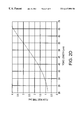
- FIG. 2D is a representative graph of a relationship between yoke length and flux rise time
- FIG. 3 is a process diagram of a method for forming a write element of the prior art
- FIG. 4A is a cross-sectional side view of a write element, according to an embodiment of the present invention.
- FIG. 4B is an ABS view taken along line 4 B— 4 B of FIG. 4A.
- FIG. 5 is a process diagram of a method for forming a write element, according to an embodiment of the present invention.
- FIGS. 1A, 1 B, 2 A-C, and 3 were discussed with reference to the prior art.
- FIG. 4A is a cross-sectional side view of a read/write head 70 according to an embodiment of the present invention.
- FIG. 4B is an ABS view of the read/write head 70 taken along line 4 B— 4 B of FIG. 4 A.
- the read/write head 70 includes a read element 26 and a write element 84 disposed above a substrate 25 .
- the read element 26 of the read/write head 70 includes a read sensor 34 in a dielectric medium 35 that is disposed between first and second shields 30 , 32 .
- the read element 26 is defined by side surfaces 71 (one shown in FIG. 4 A and two others shown in FIG. 4 B).
- a planar top surface 73 of the second shield 32 which lies substantially in a plane 74 , further defines the read element 26 .
- the read/write head 70 also includes a buildup insulation layer 72 . More specifically, the buildup insulation layer 72 is disposed adjacent the read element side surfaces 71 . In addition, the buildup insulation layer 72 has a substantially planar top surface 76 which also lies substantially in the plane 74 . Thus, the first pole upper surface 73 and the buildup insulation layer upper surface 76 are substantially co-planar.
- the buildup insulation layer 72 can be formed of any suitable electrically insulating, non-magnetic material, for example alumina, (Al 2 O 3 ).
- a write gap material layer 78 is disposed above the second shield 32 , which operates as a first pole of the write element 84 , and above the buildup insulation layer 72 .
- the write gap material layer 78 can be formed of any suitable non-magnetic, electrically insulating material, such as alumina. Because the first pole upper surface 73 and buildup insulation layer upper surface 76 are substantially co-planar, the write gap material layer 78 is substantially planar.
- a coil layer 80 including multiple coil winds 81 , is disposed above the write gap material layer 78 .
- the coil layer 80 can be formed of any suitable conductive material, such as copper.
- Above and surrounding coil layer 80 is a coil insulation layer 82 formed of any suitable electrically insulating material, such as photoresistive material. Of course, other alternating layers of coil and insulation can also be included above the coil insulation layer 82 in alternative embodiments of the present invention.
- Completing the write element 84 of the present invention is a second pole 86 formed above the write gap material layer 78 , and over the coil layer 80 and coil insulation layer 82 .
- the second pole 86 extends from the ABS to, and including, the backgap portion 40 which connects to the first pole 32 .
- the second pole 86 can be formed of the same or similar material as the first pole 32 , or any other suitable magnetic material, for example NiFe.
- the coil layer 80 can be formed with a wind pitch P of less than 3 microns, as is further discussed below with respect to FIG. 5 .
- the coil insulation layer 82 can be formed to cover the coil layer 80 , while having an maximum height Hi that is less than in typical write elements of the prior art.
- the topography over which the second pole is disposed is lower, yielding a smaller stack height SH and smaller apex angle ⁇ .
- the width W 2 of the second pole 86 can be better controlled to provide a write trackwidth which supports high density applications.
- the throat height TH can be better controlled to provide increased writing performance.
- FIG. 5 is a process diagram for a method 90 for forming a write element according to an embodiment of the present invention.
- a first pole is provided.
- the first pole can be formed of any suitable magnetic material, such as NiFe.
- An insulating layer is formed in operation 94 covering the first pole that is provided in operation 92 .
- the insulating layer can be formed of any suitable material such as alumina.
- Operation 96 includes planarizing the insulation layer formed in operation 94 , thereby exposing the first pole and forming a buildup insulation layer.
- an upper surface of the first pole and an upper surface of the buildup insulation layer are substantially planar and in substantially the same plane.
- This planarization can be accomplished using suitable techniques such as chemical-mechanical polishing (CMP), with substantially no critical tolerances.
- CMP chemical-mechanical polishing
- Such a process can be quicker and less expensive than other prior art methods employed to yield higher performance write elements, such as focused ion beam (FIB) milling as discussed above.
- FIB focused ion beam
- a write gap material layer is formed above the first pole and the buildup insulation layer. Because the upper surface of the buildup insulation layer and the upper surface of the first pole are substantially planar and in substantially the same plane due to the planarization in operation 96 , the write gap material layer is also substantially planar. Formation of the write gap material layer can also include formation of a backgap via which extends through the write gap material layer and exposes the first pole.
- a coil layer is formed in operation 100 above the write gap material layer of operation 98 .
- This coil layer can be formed by first depositing and patterning photoresistive material over the write gap material layer. Because the write gap material layer is substantially planar, the photoresistive material can be more easily patterned with consistent dimensions throughout. A conductive material, such as copper, can then be plated in conjunction with the patterned photoresist. After removal of the photoresistive material, the first coil remains, formed of a plurality of coil winds having a particular pitch P which define the wind-to-wind spacing. Because of the planar deposition of the photoresistive material, the pattern dimension consistency is substantially not affected by increased wind height.
- the wind height can be greater than about 1 micron and, further, greater than about 2 microns. More specifically, the wind height can be in the range of about 1 micron to about 4 microns. Such larger wind height can reduce the coil resistance due to enlarging coil cross-section, and thereby the thermal Johnson noise can be largely reduced.
- the pitch of the coil winds between the first and second pole can be substantially equal to a minimum that is desired to produce a desired yield of non-shorting coil layers.
- the pitch of the coil winds between the poles can be smaller in the present invention than in the described prior art.
- the coil wind pitch can be less than one micron in the present invention.
- more winds can be included between the first and second poles than in the prior art.
- about nine coil winds can be included between the first and second poles which produces a large gap field for magnetic recording density over 10 Gb/in 2 .
- the yoke length can be shorter than in the prior art, and therefore exhibit a faster flux rise time. Also, with a smaller yoke length providing the same gap field as in the prior art, a smaller head inductance can be experienced. Because of this and with concomitant better impedance matching, such a write element can be used in conjunction with a preamp chip-on-suspension with a current rise time that is less than in the prior art. With such reduced current rise time, the write element of the present invention can be utilized in high data rate applications, such as 1 Gb/sec.
- a coil insulation layer is formed above and surrounding the first coil layer that was formed in operation 100 .
- the coil insulation layer can be formed of any suitable electrically insulating and non-magnetic material, such as photoresistive material. Because the coil layer is substantially planar, the coil insulation layer can have a maximum height that is smaller than would be needed to cover a non-planar coil layer.
- the coil insulation layer of the present invention can be about 1.5 microns above the coil layer, with a maximum height of about 2 microns.
- a second pole is formed above the coil insulation layer in operation 104 .
- the second pole can extend through the backgap via formed in operation 98 , thereby forming a backgap portion in contact with the first pole.
- Forming the second pole can include depositing and patterning photoresistive material above and over the write gap material layer, and the coil insulation layer. Because the write gap material layer and coil layer are substantially planar, and the coil insulation layer has a smaller height than in the prior art, and therefore the apex angle is smaller, the patterning of the photoresistive material can be more precise.
- the coil insulation height can typically be about 12.5 microns
- this dimension can be about 2 microns.
- the trackwidth and throat height defined by the resulting second pole is more precisely controlled to provide greater write performance.
- trackwidths of less than 0.7 microns can be achieved to support applications of up to about 20 Gb/in. 2 data density.
- more precise control of the trackwidth can contribute to a more precisely defined track density which improves mass production yield of high density recording heads.
- the present invention provides structures and methods for providing a magnetoresistive write element that has more precisely defined trackwidth and throat height and smaller coil wind pitch, and therefore exhibits increased write performance over previous write elements.
- the invention has been described herein in terms of several preferred embodiments. Other embodiments of the invention, including alternatives, modifications, permutations and equivalents of the embodiments described herein, will be apparent to those skilled in the art from consideration of the specification, study of the drawings, and practice of the invention.
- the above described write element can be incorporated with a read element to provide a read/write head, or further incorporated with other components of a disk drive system.
- the embodiments and preferred features described above should be considered exemplary, with the invention being defined by the appended claims, which therefore include all such alternatives, modifications, permutations and equivalents as fall within the true spirit and scope of the present invention.
Abstract
Description
Claims (34)
Priority Applications (1)
| Application Number | Priority Date | Filing Date | Title |
|---|---|---|---|
| US09/274,187 US6417998B1 (en) | 1999-03-23 | 1999-03-23 | Ultra small advanced write transducer and method for making same |
Applications Claiming Priority (1)
| Application Number | Priority Date | Filing Date | Title |
|---|---|---|---|
| US09/274,187 US6417998B1 (en) | 1999-03-23 | 1999-03-23 | Ultra small advanced write transducer and method for making same |
Publications (1)
| Publication Number | Publication Date |
|---|---|
| US6417998B1 true US6417998B1 (en) | 2002-07-09 |
Family
ID=23047149
Family Applications (1)
| Application Number | Title | Priority Date | Filing Date |
|---|---|---|---|
| US09/274,187 Expired - Lifetime US6417998B1 (en) | 1999-03-23 | 1999-03-23 | Ultra small advanced write transducer and method for making same |
Country Status (1)
| Country | Link |
|---|---|
| US (1) | US6417998B1 (en) |
Cited By (132)
| Publication number | Priority date | Publication date | Assignee | Title |
|---|---|---|---|---|
| US20040085685A1 (en) * | 1998-08-20 | 2004-05-06 | Yoshihiro Shiroishi | Magnetic recording and reading device |
| US7310204B1 (en) | 2003-12-19 | 2007-12-18 | Western Digital (Fremont), Llc | Inductive writer design for using a soft magnetic pedestal having a high magnetic saturation layer |
| US8830628B1 (en) | 2009-02-23 | 2014-09-09 | Western Digital (Fremont), Llc | Method and system for providing a perpendicular magnetic recording head |
| US8879207B1 (en) | 2011-12-20 | 2014-11-04 | Western Digital (Fremont), Llc | Method for providing a side shield for a magnetic recording transducer using an air bridge |
| US8883017B1 (en) | 2013-03-12 | 2014-11-11 | Western Digital (Fremont), Llc | Method and system for providing a read transducer having seamless interfaces |
| US8917581B1 (en) | 2013-12-18 | 2014-12-23 | Western Digital Technologies, Inc. | Self-anneal process for a near field transducer and chimney in a hard disk drive assembly |
| US8923102B1 (en) | 2013-07-16 | 2014-12-30 | Western Digital (Fremont), Llc | Optical grating coupling for interferometric waveguides in heat assisted magnetic recording heads |
| US8947985B1 (en) | 2013-07-16 | 2015-02-03 | Western Digital (Fremont), Llc | Heat assisted magnetic recording transducers having a recessed pole |
| US8953422B1 (en) | 2014-06-10 | 2015-02-10 | Western Digital (Fremont), Llc | Near field transducer using dielectric waveguide core with fine ridge feature |
| US8958272B1 (en) | 2014-06-10 | 2015-02-17 | Western Digital (Fremont), Llc | Interfering near field transducer for energy assisted magnetic recording |
| US8971160B1 (en) | 2013-12-19 | 2015-03-03 | Western Digital (Fremont), Llc | Near field transducer with high refractive index pin for heat assisted magnetic recording |
| US8970988B1 (en) | 2013-12-31 | 2015-03-03 | Western Digital (Fremont), Llc | Electric gaps and method for making electric gaps for multiple sensor arrays |
| US8976635B1 (en) | 2014-06-10 | 2015-03-10 | Western Digital (Fremont), Llc | Near field transducer driven by a transverse electric waveguide for energy assisted magnetic recording |
| US8980109B1 (en) | 2012-12-11 | 2015-03-17 | Western Digital (Fremont), Llc | Method for providing a magnetic recording transducer using a combined main pole and side shield CMP for a wraparound shield scheme |
| US8982508B1 (en) | 2011-10-31 | 2015-03-17 | Western Digital (Fremont), Llc | Method for providing a side shield for a magnetic recording transducer |
| US8984740B1 (en) | 2012-11-30 | 2015-03-24 | Western Digital (Fremont), Llc | Process for providing a magnetic recording transducer having a smooth magnetic seed layer |
| US8988812B1 (en) | 2013-11-27 | 2015-03-24 | Western Digital (Fremont), Llc | Multi-sensor array configuration for a two-dimensional magnetic recording (TDMR) operation |
| US8988825B1 (en) | 2014-02-28 | 2015-03-24 | Western Digital (Fremont, LLC | Method for fabricating a magnetic writer having half-side shields |
| US8995087B1 (en) | 2006-11-29 | 2015-03-31 | Western Digital (Fremont), Llc | Perpendicular magnetic recording write head having a wrap around shield |
| US8993217B1 (en) | 2013-04-04 | 2015-03-31 | Western Digital (Fremont), Llc | Double exposure technique for high resolution disk imaging |
| US9001467B1 (en) | 2014-03-05 | 2015-04-07 | Western Digital (Fremont), Llc | Method for fabricating side shields in a magnetic writer |
| US8997832B1 (en) | 2010-11-23 | 2015-04-07 | Western Digital (Fremont), Llc | Method of fabricating micrometer scale components |
| US9001628B1 (en) | 2013-12-16 | 2015-04-07 | Western Digital (Fremont), Llc | Assistant waveguides for evaluating main waveguide coupling efficiency and diode laser alignment tolerances for hard disk |
| US9007719B1 (en) | 2013-10-23 | 2015-04-14 | Western Digital (Fremont), Llc | Systems and methods for using double mask techniques to achieve very small features |
| US9007879B1 (en) | 2014-06-10 | 2015-04-14 | Western Digital (Fremont), Llc | Interfering near field transducer having a wide metal bar feature for energy assisted magnetic recording |
| US9007725B1 (en) | 2014-10-07 | 2015-04-14 | Western Digital (Fremont), Llc | Sensor with positive coupling between dual ferromagnetic free layer laminates |
| US9013836B1 (en) | 2013-04-02 | 2015-04-21 | Western Digital (Fremont), Llc | Method and system for providing an antiferromagnetically coupled return pole |
| US9042058B1 (en) | 2013-10-17 | 2015-05-26 | Western Digital Technologies, Inc. | Shield designed for middle shields in a multiple sensor array |
| US9042208B1 (en) | 2013-03-11 | 2015-05-26 | Western Digital Technologies, Inc. | Disk drive measuring fly height by applying a bias voltage to an electrically insulated write component of a head |
| US9042057B1 (en) | 2013-01-09 | 2015-05-26 | Western Digital (Fremont), Llc | Methods for providing magnetic storage elements with high magneto-resistance using Heusler alloys |
| US9042052B1 (en) | 2014-06-23 | 2015-05-26 | Western Digital (Fremont), Llc | Magnetic writer having a partially shunted coil |
| US9042051B2 (en) | 2013-08-15 | 2015-05-26 | Western Digital (Fremont), Llc | Gradient write gap for perpendicular magnetic recording writer |
| US9053735B1 (en) | 2014-06-20 | 2015-06-09 | Western Digital (Fremont), Llc | Method for fabricating a magnetic writer using a full-film metal planarization |
| US9064527B1 (en) | 2013-04-12 | 2015-06-23 | Western Digital (Fremont), Llc | High order tapered waveguide for use in a heat assisted magnetic recording head |
| US9065043B1 (en) | 2012-06-29 | 2015-06-23 | Western Digital (Fremont), Llc | Tunnel magnetoresistance read head with narrow shield-to-shield spacing |
| US9064528B1 (en) | 2013-05-17 | 2015-06-23 | Western Digital Technologies, Inc. | Interferometric waveguide usable in shingled heat assisted magnetic recording in the absence of a near-field transducer |
| US9064507B1 (en) | 2009-07-31 | 2015-06-23 | Western Digital (Fremont), Llc | Magnetic etch-stop layer for magnetoresistive read heads |
| US9070381B1 (en) | 2013-04-12 | 2015-06-30 | Western Digital (Fremont), Llc | Magnetic recording read transducer having a laminated free layer |
| US9082423B1 (en) | 2013-12-18 | 2015-07-14 | Western Digital (Fremont), Llc | Magnetic recording write transducer having an improved trailing surface profile |
| US9087527B1 (en) | 2014-10-28 | 2015-07-21 | Western Digital (Fremont), Llc | Apparatus and method for middle shield connection in magnetic recording transducers |
| US9087534B1 (en) | 2011-12-20 | 2015-07-21 | Western Digital (Fremont), Llc | Method and system for providing a read transducer having soft and hard magnetic bias structures |
| US9093639B2 (en) | 2012-02-21 | 2015-07-28 | Western Digital (Fremont), Llc | Methods for manufacturing a magnetoresistive structure utilizing heating and cooling |
| US9104107B1 (en) | 2013-04-03 | 2015-08-11 | Western Digital (Fremont), Llc | DUV photoresist process |
| US9111558B1 (en) | 2014-03-14 | 2015-08-18 | Western Digital (Fremont), Llc | System and method of diffractive focusing of light in a waveguide |
| US9111550B1 (en) | 2014-12-04 | 2015-08-18 | Western Digital (Fremont), Llc | Write transducer having a magnetic buffer layer spaced between a side shield and a write pole by non-magnetic layers |
| US9111564B1 (en) | 2013-04-02 | 2015-08-18 | Western Digital (Fremont), Llc | Magnetic recording writer having a main pole with multiple flare angles |
| US9123358B1 (en) | 2012-06-11 | 2015-09-01 | Western Digital (Fremont), Llc | Conformal high moment side shield seed layer for perpendicular magnetic recording writer |
| US9123359B1 (en) | 2010-12-22 | 2015-09-01 | Western Digital (Fremont), Llc | Magnetic recording transducer with sputtered antiferromagnetic coupling trilayer between plated ferromagnetic shields and method of fabrication |
| US9123374B1 (en) | 2015-02-12 | 2015-09-01 | Western Digital (Fremont), Llc | Heat assisted magnetic recording writer having an integrated polarization rotation plate |
| US9123362B1 (en) | 2011-03-22 | 2015-09-01 | Western Digital (Fremont), Llc | Methods for assembling an electrically assisted magnetic recording (EAMR) head |
| US9135930B1 (en) | 2014-03-06 | 2015-09-15 | Western Digital (Fremont), Llc | Method for fabricating a magnetic write pole using vacuum deposition |
| US9135937B1 (en) | 2014-05-09 | 2015-09-15 | Western Digital (Fremont), Llc | Current modulation on laser diode for energy assisted magnetic recording transducer |
| US9142233B1 (en) | 2014-02-28 | 2015-09-22 | Western Digital (Fremont), Llc | Heat assisted magnetic recording writer having a recessed pole |
| US9147408B1 (en) | 2013-12-19 | 2015-09-29 | Western Digital (Fremont), Llc | Heated AFM layer deposition and cooling process for TMR magnetic recording sensor with high pinning field |
| US9147404B1 (en) | 2015-03-31 | 2015-09-29 | Western Digital (Fremont), Llc | Method and system for providing a read transducer having a dual free layer |
| US9153255B1 (en) | 2014-03-05 | 2015-10-06 | Western Digital (Fremont), Llc | Method for fabricating a magnetic writer having an asymmetric gap and shields |
| US9183854B2 (en) | 2014-02-24 | 2015-11-10 | Western Digital (Fremont), Llc | Method to make interferometric taper waveguide for HAMR light delivery |
| US9190079B1 (en) | 2014-09-22 | 2015-11-17 | Western Digital (Fremont), Llc | Magnetic write pole having engineered radius of curvature and chisel angle profiles |
| US9190085B1 (en) | 2014-03-12 | 2015-11-17 | Western Digital (Fremont), Llc | Waveguide with reflective grating for localized energy intensity |
| US9194692B1 (en) | 2013-12-06 | 2015-11-24 | Western Digital (Fremont), Llc | Systems and methods for using white light interferometry to measure undercut of a bi-layer structure |
| US9202480B2 (en) | 2009-10-14 | 2015-12-01 | Western Digital (Fremont), LLC. | Double patterning hard mask for damascene perpendicular magnetic recording (PMR) writer |
| US9202493B1 (en) | 2014-02-28 | 2015-12-01 | Western Digital (Fremont), Llc | Method of making an ultra-sharp tip mode converter for a HAMR head |
| US9213322B1 (en) | 2012-08-16 | 2015-12-15 | Western Digital (Fremont), Llc | Methods for providing run to run process control using a dynamic tuner |
| US9214165B1 (en) | 2014-12-18 | 2015-12-15 | Western Digital (Fremont), Llc | Magnetic writer having a gradient in saturation magnetization of the shields |
| US9214172B2 (en) | 2013-10-23 | 2015-12-15 | Western Digital (Fremont), Llc | Method of manufacturing a magnetic read head |
| US9214169B1 (en) | 2014-06-20 | 2015-12-15 | Western Digital (Fremont), Llc | Magnetic recording read transducer having a laminated free layer |
| US9230565B1 (en) | 2014-06-24 | 2016-01-05 | Western Digital (Fremont), Llc | Magnetic shield for magnetic recording head |
| US9236560B1 (en) | 2014-12-08 | 2016-01-12 | Western Digital (Fremont), Llc | Spin transfer torque tunneling magnetoresistive device having a laminated free layer with perpendicular magnetic anisotropy |
| US9245562B1 (en) | 2015-03-30 | 2016-01-26 | Western Digital (Fremont), Llc | Magnetic recording writer with a composite main pole |
| US9245545B1 (en) | 2013-04-12 | 2016-01-26 | Wester Digital (Fremont), Llc | Short yoke length coils for magnetic heads in disk drives |
| US9245543B1 (en) | 2010-06-25 | 2016-01-26 | Western Digital (Fremont), Llc | Method for providing an energy assisted magnetic recording head having a laser integrally mounted to the slider |
| US9251813B1 (en) | 2009-04-19 | 2016-02-02 | Western Digital (Fremont), Llc | Method of making a magnetic recording head |
| US9263067B1 (en) | 2013-05-29 | 2016-02-16 | Western Digital (Fremont), Llc | Process for making PMR writer with constant side wall angle |
| US9263071B1 (en) | 2015-03-31 | 2016-02-16 | Western Digital (Fremont), Llc | Flat NFT for heat assisted magnetic recording |
| US9269382B1 (en) | 2012-06-29 | 2016-02-23 | Western Digital (Fremont), Llc | Method and system for providing a read transducer having improved pinning of the pinned layer at higher recording densities |
| US9275657B1 (en) | 2013-08-14 | 2016-03-01 | Western Digital (Fremont), Llc | Process for making PMR writer with non-conformal side gaps |
| US9280990B1 (en) | 2013-12-11 | 2016-03-08 | Western Digital (Fremont), Llc | Method for fabricating a magnetic writer using multiple etches |
| US9287494B1 (en) | 2013-06-28 | 2016-03-15 | Western Digital (Fremont), Llc | Magnetic tunnel junction (MTJ) with a magnesium oxide tunnel barrier |
| US9286919B1 (en) | 2014-12-17 | 2016-03-15 | Western Digital (Fremont), Llc | Magnetic writer having a dual side gap |
| US9305583B1 (en) | 2014-02-18 | 2016-04-05 | Western Digital (Fremont), Llc | Method for fabricating a magnetic writer using multiple etches of damascene materials |
| US9312064B1 (en) | 2015-03-02 | 2016-04-12 | Western Digital (Fremont), Llc | Method to fabricate a magnetic head including ion milling of read gap using dual layer hard mask |
| US9318130B1 (en) | 2013-07-02 | 2016-04-19 | Western Digital (Fremont), Llc | Method to fabricate tunneling magnetic recording heads with extended pinned layer |
| US9336814B1 (en) | 2013-03-12 | 2016-05-10 | Western Digital (Fremont), Llc | Inverse tapered waveguide for use in a heat assisted magnetic recording head |
| US9343098B1 (en) | 2013-08-23 | 2016-05-17 | Western Digital (Fremont), Llc | Method for providing a heat assisted magnetic recording transducer having protective pads |
| US9343087B1 (en) | 2014-12-21 | 2016-05-17 | Western Digital (Fremont), Llc | Method for fabricating a magnetic writer having half shields |
| US9343086B1 (en) | 2013-09-11 | 2016-05-17 | Western Digital (Fremont), Llc | Magnetic recording write transducer having an improved sidewall angle profile |
| US9349394B1 (en) | 2013-10-18 | 2016-05-24 | Western Digital (Fremont), Llc | Method for fabricating a magnetic writer having a gradient side gap |
| US9349392B1 (en) | 2012-05-24 | 2016-05-24 | Western Digital (Fremont), Llc | Methods for improving adhesion on dielectric substrates |
| US9361913B1 (en) | 2013-06-03 | 2016-06-07 | Western Digital (Fremont), Llc | Recording read heads with a multi-layer AFM layer methods and apparatuses |
| US9361914B1 (en) | 2014-06-18 | 2016-06-07 | Western Digital (Fremont), Llc | Magnetic sensor with thin capping layer |
| US9368134B1 (en) | 2010-12-16 | 2016-06-14 | Western Digital (Fremont), Llc | Method and system for providing an antiferromagnetically coupled writer |
| US9384763B1 (en) | 2015-03-26 | 2016-07-05 | Western Digital (Fremont), Llc | Dual free layer magnetic reader having a rear bias structure including a soft bias layer |
| US9384765B1 (en) | 2015-09-24 | 2016-07-05 | Western Digital (Fremont), Llc | Method and system for providing a HAMR writer having improved optical efficiency |
| US9396743B1 (en) | 2014-02-28 | 2016-07-19 | Western Digital (Fremont), Llc | Systems and methods for controlling soft bias thickness for tunnel magnetoresistance readers |
| US9396742B1 (en) | 2012-11-30 | 2016-07-19 | Western Digital (Fremont), Llc | Magnetoresistive sensor for a magnetic storage system read head, and fabrication method thereof |
| US9406331B1 (en) | 2013-06-17 | 2016-08-02 | Western Digital (Fremont), Llc | Method for making ultra-narrow read sensor and read transducer device resulting therefrom |
| US9424866B1 (en) | 2015-09-24 | 2016-08-23 | Western Digital (Fremont), Llc | Heat assisted magnetic recording write apparatus having a dielectric gap |
| US9431039B1 (en) | 2013-05-21 | 2016-08-30 | Western Digital (Fremont), Llc | Multiple sensor array usable in two-dimensional magnetic recording |
| US9431038B1 (en) | 2015-06-29 | 2016-08-30 | Western Digital (Fremont), Llc | Method for fabricating a magnetic write pole having an improved sidewall angle profile |
| US9431032B1 (en) | 2013-08-14 | 2016-08-30 | Western Digital (Fremont), Llc | Electrical connection arrangement for a multiple sensor array usable in two-dimensional magnetic recording |
| US9431031B1 (en) | 2015-03-24 | 2016-08-30 | Western Digital (Fremont), Llc | System and method for magnetic transducers having multiple sensors and AFC shields |
| US9431047B1 (en) | 2013-05-01 | 2016-08-30 | Western Digital (Fremont), Llc | Method for providing an improved AFM reader shield |
| US9437251B1 (en) | 2014-12-22 | 2016-09-06 | Western Digital (Fremont), Llc | Apparatus and method having TDMR reader to reader shunts |
| US9443541B1 (en) | 2015-03-24 | 2016-09-13 | Western Digital (Fremont), Llc | Magnetic writer having a gradient in saturation magnetization of the shields and return pole |
| US9441938B1 (en) | 2013-10-08 | 2016-09-13 | Western Digital (Fremont), Llc | Test structures for measuring near field transducer disc length |
| US9449625B1 (en) | 2014-12-24 | 2016-09-20 | Western Digital (Fremont), Llc | Heat assisted magnetic recording head having a plurality of diffusion barrier layers |
| US9449621B1 (en) | 2015-03-26 | 2016-09-20 | Western Digital (Fremont), Llc | Dual free layer magnetic reader having a rear bias structure having a high aspect ratio |
| US9472216B1 (en) | 2015-09-23 | 2016-10-18 | Western Digital (Fremont), Llc | Differential dual free layer magnetic reader |
| US9484051B1 (en) | 2015-11-09 | 2016-11-01 | The Provost, Fellows, Foundation Scholars and the other members of Board, of the College of the Holy and Undivided Trinity of Queen Elizabeth near Dublin | Method and system for reducing undesirable reflections in a HAMR write apparatus |
| US9508365B1 (en) | 2015-06-24 | 2016-11-29 | Western Digital (Fremont), LLC. | Magnetic reader having a crystal decoupling structure |
| US9508363B1 (en) | 2014-06-17 | 2016-11-29 | Western Digital (Fremont), Llc | Method for fabricating a magnetic write pole having a leading edge bevel |
| US9508372B1 (en) | 2015-06-03 | 2016-11-29 | Western Digital (Fremont), Llc | Shingle magnetic writer having a low sidewall angle pole |
| US9530443B1 (en) | 2015-06-25 | 2016-12-27 | Western Digital (Fremont), Llc | Method for fabricating a magnetic recording device having a high aspect ratio structure |
| US9564150B1 (en) | 2015-11-24 | 2017-02-07 | Western Digital (Fremont), Llc | Magnetic read apparatus having an improved read sensor isolation circuit |
| US9595273B1 (en) | 2015-09-30 | 2017-03-14 | Western Digital (Fremont), Llc | Shingle magnetic writer having nonconformal shields |
| US9646639B2 (en) | 2015-06-26 | 2017-05-09 | Western Digital (Fremont), Llc | Heat assisted magnetic recording writer having integrated polarization rotation waveguides |
| US9666214B1 (en) | 2015-09-23 | 2017-05-30 | Western Digital (Fremont), Llc | Free layer magnetic reader that may have a reduced shield-to-shield spacing |
| US9721595B1 (en) | 2014-12-04 | 2017-08-01 | Western Digital (Fremont), Llc | Method for providing a storage device |
| US9740805B1 (en) | 2015-12-01 | 2017-08-22 | Western Digital (Fremont), Llc | Method and system for detecting hotspots for photolithographically-defined devices |
| US9741366B1 (en) | 2014-12-18 | 2017-08-22 | Western Digital (Fremont), Llc | Method for fabricating a magnetic writer having a gradient in saturation magnetization of the shields |
| US9754611B1 (en) | 2015-11-30 | 2017-09-05 | Western Digital (Fremont), Llc | Magnetic recording write apparatus having a stepped conformal trailing shield |
| US9767831B1 (en) | 2015-12-01 | 2017-09-19 | Western Digital (Fremont), Llc | Magnetic writer having convex trailing surface pole and conformal write gap |
| US9786301B1 (en) | 2014-12-02 | 2017-10-10 | Western Digital (Fremont), Llc | Apparatuses and methods for providing thin shields in a multiple sensor array |
| US9799351B1 (en) | 2015-11-30 | 2017-10-24 | Western Digital (Fremont), Llc | Short yoke length writer having assist coils |
| US9812155B1 (en) | 2015-11-23 | 2017-11-07 | Western Digital (Fremont), Llc | Method and system for fabricating high junction angle read sensors |
| US9842615B1 (en) | 2015-06-26 | 2017-12-12 | Western Digital (Fremont), Llc | Magnetic reader having a nonmagnetic insertion layer for the pinning layer |
| US9858951B1 (en) | 2015-12-01 | 2018-01-02 | Western Digital (Fremont), Llc | Method for providing a multilayer AFM layer in a read sensor |
| US9881638B1 (en) | 2014-12-17 | 2018-01-30 | Western Digital (Fremont), Llc | Method for providing a near-field transducer (NFT) for a heat assisted magnetic recording (HAMR) device |
| US9934811B1 (en) | 2014-03-07 | 2018-04-03 | Western Digital (Fremont), Llc | Methods for controlling stray fields of magnetic features using magneto-elastic anisotropy |
| US9953670B1 (en) | 2015-11-10 | 2018-04-24 | Western Digital (Fremont), Llc | Method and system for providing a HAMR writer including a multi-mode interference device |
| US10037770B1 (en) | 2015-11-12 | 2018-07-31 | Western Digital (Fremont), Llc | Method for providing a magnetic recording write apparatus having a seamless pole |
| US10074387B1 (en) | 2014-12-21 | 2018-09-11 | Western Digital (Fremont), Llc | Method and system for providing a read transducer having symmetric antiferromagnetically coupled shields |
Citations (28)
| Publication number | Priority date | Publication date | Assignee | Title |
|---|---|---|---|---|
| US4677036A (en) | 1985-01-29 | 1987-06-30 | Sharp Kabushiki Kaisha | Method of production of thin film magnetic head and magnetic head |
| US4791719A (en) | 1983-12-22 | 1988-12-20 | Hitachi, Ltd. | Method of manufacturing a thin-film magnetic head |
| US4816946A (en) * | 1982-11-26 | 1989-03-28 | Sharp Kabushiki Kaisha | Method of manufacturing thin film magnetic head |
| US5045961A (en) | 1984-07-25 | 1991-09-03 | Hitachi, Ltd. | Thin film magnetic head |
| US5161299A (en) | 1990-12-26 | 1992-11-10 | International Business Machines Corporation | Method of making a magnetic hybrid interleaved head |
| US5189580A (en) | 1989-06-30 | 1993-02-23 | Ampex Corporation | Ultra small track width thin film magnetic transducer |
| US5224003A (en) | 1988-06-28 | 1993-06-29 | Matsushita Electric Industrial Co., Ltd. | Thin-film magnetic head with lead isolated from upper magnetic block |
| US5241440A (en) * | 1989-08-23 | 1993-08-31 | Hitachi, Ltd. | Thin film magnetic head and manufacturing method therefor |
| US5270895A (en) | 1991-07-05 | 1993-12-14 | U.S. Philips Corporation | Combined read/write thin-film magnetic head with composite shared flux guide |
| US5282308A (en) | 1992-12-29 | 1994-02-01 | International Business Machines Corporation | Thin film planarization process for fabricating magnetic heads employing a stitched pole structure |
| US5283942A (en) | 1992-12-29 | 1994-02-08 | International Business Machines Corporation | Sacrificial layer planarization process for fabricating a narrow thin film inductive head |
| US5406695A (en) | 1992-10-30 | 1995-04-18 | Fujitsu Ltd. | Method for fabricating thin-film magnetic heads |
| US5435053A (en) | 1994-03-02 | 1995-07-25 | International Business Machines Corporation | Simplified method of making merged MR head |
| US5448822A (en) * | 1993-03-10 | 1995-09-12 | Quantum Corporation | Method of making a thin film magnetic head having multi-layer coils |
| US5546650A (en) | 1994-06-22 | 1996-08-20 | Storage Technology Corporation | Method of manufacturing a multiple track thin film recording head |
| US5576098A (en) | 1992-07-08 | 1996-11-19 | Fuji Electric Co., Ltd. | Thin film magnetic head |
| US5581429A (en) | 1994-04-07 | 1996-12-03 | Hitachi Metals, Ltd. | Thin-film magnetic head having improved magnetic pole structure |
| US5621596A (en) | 1994-08-25 | 1997-04-15 | International Business Machines Corporation | Low profile thin film write head |
| US5649351A (en) | 1994-02-08 | 1997-07-22 | International Business Machines Corporation | Method of making thin film magnetic write head |
| US5691861A (en) | 1995-06-15 | 1997-11-25 | Fujitsu Limited | Actuator arm assembly having side wall projection for carrying juxtaposed head wires |
| US5722157A (en) | 1995-06-28 | 1998-03-03 | Yamaha Corporation | Method of making an induction and magnetoresistance type composite magnetic head |
| US5751522A (en) * | 1993-10-21 | 1998-05-12 | Alps Electric Co., Ltd. | Combined-type thin film magnetic head with inductive magnetic head having low-inductive core |
| US5828522A (en) * | 1994-09-13 | 1998-10-27 | International Business Machines Corporation | Velocity control of head load/unload mechanism in a disk drive using dither |
| US5923506A (en) * | 1997-10-03 | 1999-07-13 | Storage Technology Corporation | Recording head element with improved coil tap and method for manufacturing same |
| US6002555A (en) * | 1997-09-10 | 1999-12-14 | Fujitsu Limited | Thin film magnetic head |
| US6043959A (en) * | 1998-03-23 | 2000-03-28 | Read-Rite Corporation | Inductive write head formed with flat yoke and merged with magnetoresistive read transducer |
| US6088197A (en) * | 1997-07-30 | 2000-07-11 | Nec Corporation | Thin film magnetic head with reduced-area common pole layer for improving recording density |
| US6151193A (en) * | 1997-05-27 | 2000-11-21 | Tdk Corporation | Thin film magnetic head |
-
1999
- 1999-03-23 US US09/274,187 patent/US6417998B1/en not_active Expired - Lifetime
Patent Citations (29)
| Publication number | Priority date | Publication date | Assignee | Title |
|---|---|---|---|---|
| US4816946A (en) * | 1982-11-26 | 1989-03-28 | Sharp Kabushiki Kaisha | Method of manufacturing thin film magnetic head |
| US4791719A (en) | 1983-12-22 | 1988-12-20 | Hitachi, Ltd. | Method of manufacturing a thin-film magnetic head |
| US5045961A (en) | 1984-07-25 | 1991-09-03 | Hitachi, Ltd. | Thin film magnetic head |
| US4677036A (en) | 1985-01-29 | 1987-06-30 | Sharp Kabushiki Kaisha | Method of production of thin film magnetic head and magnetic head |
| US5224003A (en) | 1988-06-28 | 1993-06-29 | Matsushita Electric Industrial Co., Ltd. | Thin-film magnetic head with lead isolated from upper magnetic block |
| US5189580A (en) | 1989-06-30 | 1993-02-23 | Ampex Corporation | Ultra small track width thin film magnetic transducer |
| US5241440A (en) * | 1989-08-23 | 1993-08-31 | Hitachi, Ltd. | Thin film magnetic head and manufacturing method therefor |
| US5161299A (en) | 1990-12-26 | 1992-11-10 | International Business Machines Corporation | Method of making a magnetic hybrid interleaved head |
| US5270895A (en) | 1991-07-05 | 1993-12-14 | U.S. Philips Corporation | Combined read/write thin-film magnetic head with composite shared flux guide |
| US5576098A (en) | 1992-07-08 | 1996-11-19 | Fuji Electric Co., Ltd. | Thin film magnetic head |
| US5406695A (en) | 1992-10-30 | 1995-04-18 | Fujitsu Ltd. | Method for fabricating thin-film magnetic heads |
| US5282308A (en) | 1992-12-29 | 1994-02-01 | International Business Machines Corporation | Thin film planarization process for fabricating magnetic heads employing a stitched pole structure |
| US5283942A (en) | 1992-12-29 | 1994-02-08 | International Business Machines Corporation | Sacrificial layer planarization process for fabricating a narrow thin film inductive head |
| US5448822A (en) * | 1993-03-10 | 1995-09-12 | Quantum Corporation | Method of making a thin film magnetic head having multi-layer coils |
| US5751522A (en) * | 1993-10-21 | 1998-05-12 | Alps Electric Co., Ltd. | Combined-type thin film magnetic head with inductive magnetic head having low-inductive core |
| US5649351A (en) | 1994-02-08 | 1997-07-22 | International Business Machines Corporation | Method of making thin film magnetic write head |
| US5435053A (en) | 1994-03-02 | 1995-07-25 | International Business Machines Corporation | Simplified method of making merged MR head |
| US5700380A (en) | 1994-03-02 | 1997-12-23 | International Business Machines Corporation | Simplified method of making vias for merged MR head |
| US5581429A (en) | 1994-04-07 | 1996-12-03 | Hitachi Metals, Ltd. | Thin-film magnetic head having improved magnetic pole structure |
| US5546650A (en) | 1994-06-22 | 1996-08-20 | Storage Technology Corporation | Method of manufacturing a multiple track thin film recording head |
| US5621596A (en) | 1994-08-25 | 1997-04-15 | International Business Machines Corporation | Low profile thin film write head |
| US5828522A (en) * | 1994-09-13 | 1998-10-27 | International Business Machines Corporation | Velocity control of head load/unload mechanism in a disk drive using dither |
| US5691861A (en) | 1995-06-15 | 1997-11-25 | Fujitsu Limited | Actuator arm assembly having side wall projection for carrying juxtaposed head wires |
| US5722157A (en) | 1995-06-28 | 1998-03-03 | Yamaha Corporation | Method of making an induction and magnetoresistance type composite magnetic head |
| US6151193A (en) * | 1997-05-27 | 2000-11-21 | Tdk Corporation | Thin film magnetic head |
| US6088197A (en) * | 1997-07-30 | 2000-07-11 | Nec Corporation | Thin film magnetic head with reduced-area common pole layer for improving recording density |
| US6002555A (en) * | 1997-09-10 | 1999-12-14 | Fujitsu Limited | Thin film magnetic head |
| US5923506A (en) * | 1997-10-03 | 1999-07-13 | Storage Technology Corporation | Recording head element with improved coil tap and method for manufacturing same |
| US6043959A (en) * | 1998-03-23 | 2000-03-28 | Read-Rite Corporation | Inductive write head formed with flat yoke and merged with magnetoresistive read transducer |
Cited By (157)
| Publication number | Priority date | Publication date | Assignee | Title |
|---|---|---|---|---|
| US7903374B2 (en) | 1998-08-20 | 2011-03-08 | Hitachi Global Storage Technologies Japan, Ltd. | Magnetic recording and reading device |
| US20100246054A1 (en) * | 1998-08-20 | 2010-09-30 | Yoshihiro Shiroishi | Magnetic Recording And Reading Device |
| US20040085685A1 (en) * | 1998-08-20 | 2004-05-06 | Yoshihiro Shiroishi | Magnetic recording and reading device |
| US7177115B2 (en) | 1998-08-20 | 2007-02-13 | Hitachi Global Storage Technologies Japan, Ltd. | Magnetic recording and reading device |
| US7339762B2 (en) | 1998-08-20 | 2008-03-04 | Hitachi Global Storage Technologies Japan, Ltd. | Magnetic recording and reading device |
| US6819531B2 (en) * | 1998-08-20 | 2004-11-16 | Hitachi, Ltd. | Magnetic recording and reading device having 50 mb/s transfer rate |
| US7782566B2 (en) | 1998-08-20 | 2010-08-24 | Hitachi Global Storage Technologies Japan, Ltd. | Magnetic recording and reading device |
| US7375926B1 (en) | 2003-12-19 | 2008-05-20 | Western Digital (Fremont), Llc | Inductive writer design using a soft magnetic pedestal having a high magnetic saturation layer |
| US7310204B1 (en) | 2003-12-19 | 2007-12-18 | Western Digital (Fremont), Llc | Inductive writer design for using a soft magnetic pedestal having a high magnetic saturation layer |
| US8995087B1 (en) | 2006-11-29 | 2015-03-31 | Western Digital (Fremont), Llc | Perpendicular magnetic recording write head having a wrap around shield |
| US8830628B1 (en) | 2009-02-23 | 2014-09-09 | Western Digital (Fremont), Llc | Method and system for providing a perpendicular magnetic recording head |
| US9251813B1 (en) | 2009-04-19 | 2016-02-02 | Western Digital (Fremont), Llc | Method of making a magnetic recording head |
| US9064507B1 (en) | 2009-07-31 | 2015-06-23 | Western Digital (Fremont), Llc | Magnetic etch-stop layer for magnetoresistive read heads |
| US9202480B2 (en) | 2009-10-14 | 2015-12-01 | Western Digital (Fremont), LLC. | Double patterning hard mask for damascene perpendicular magnetic recording (PMR) writer |
| US9245543B1 (en) | 2010-06-25 | 2016-01-26 | Western Digital (Fremont), Llc | Method for providing an energy assisted magnetic recording head having a laser integrally mounted to the slider |
| US8997832B1 (en) | 2010-11-23 | 2015-04-07 | Western Digital (Fremont), Llc | Method of fabricating micrometer scale components |
| US9672847B2 (en) | 2010-11-23 | 2017-06-06 | Western Digital (Fremont), Llc | Micrometer scale components |
| US9159345B1 (en) | 2010-11-23 | 2015-10-13 | Western Digital (Fremont), Llc | Micrometer scale components |
| US9368134B1 (en) | 2010-12-16 | 2016-06-14 | Western Digital (Fremont), Llc | Method and system for providing an antiferromagnetically coupled writer |
| US9123359B1 (en) | 2010-12-22 | 2015-09-01 | Western Digital (Fremont), Llc | Magnetic recording transducer with sputtered antiferromagnetic coupling trilayer between plated ferromagnetic shields and method of fabrication |
| US9123362B1 (en) | 2011-03-22 | 2015-09-01 | Western Digital (Fremont), Llc | Methods for assembling an electrically assisted magnetic recording (EAMR) head |
| US8982508B1 (en) | 2011-10-31 | 2015-03-17 | Western Digital (Fremont), Llc | Method for providing a side shield for a magnetic recording transducer |
| US9087534B1 (en) | 2011-12-20 | 2015-07-21 | Western Digital (Fremont), Llc | Method and system for providing a read transducer having soft and hard magnetic bias structures |
| US8879207B1 (en) | 2011-12-20 | 2014-11-04 | Western Digital (Fremont), Llc | Method for providing a side shield for a magnetic recording transducer using an air bridge |
| US9093639B2 (en) | 2012-02-21 | 2015-07-28 | Western Digital (Fremont), Llc | Methods for manufacturing a magnetoresistive structure utilizing heating and cooling |
| US9940950B2 (en) | 2012-05-24 | 2018-04-10 | Western Digital (Fremont), Llc | Methods for improving adhesion on dielectric substrates |
| US9349392B1 (en) | 2012-05-24 | 2016-05-24 | Western Digital (Fremont), Llc | Methods for improving adhesion on dielectric substrates |
| US9123358B1 (en) | 2012-06-11 | 2015-09-01 | Western Digital (Fremont), Llc | Conformal high moment side shield seed layer for perpendicular magnetic recording writer |
| US9065043B1 (en) | 2012-06-29 | 2015-06-23 | Western Digital (Fremont), Llc | Tunnel magnetoresistance read head with narrow shield-to-shield spacing |
| US9412400B2 (en) | 2012-06-29 | 2016-08-09 | Western Digital (Fremont), Llc | Tunnel magnetoresistance read head with narrow shield-to-shield spacing |
| US9269382B1 (en) | 2012-06-29 | 2016-02-23 | Western Digital (Fremont), Llc | Method and system for providing a read transducer having improved pinning of the pinned layer at higher recording densities |
| US9213322B1 (en) | 2012-08-16 | 2015-12-15 | Western Digital (Fremont), Llc | Methods for providing run to run process control using a dynamic tuner |
| US9396742B1 (en) | 2012-11-30 | 2016-07-19 | Western Digital (Fremont), Llc | Magnetoresistive sensor for a magnetic storage system read head, and fabrication method thereof |
| US8984740B1 (en) | 2012-11-30 | 2015-03-24 | Western Digital (Fremont), Llc | Process for providing a magnetic recording transducer having a smooth magnetic seed layer |
| US8980109B1 (en) | 2012-12-11 | 2015-03-17 | Western Digital (Fremont), Llc | Method for providing a magnetic recording transducer using a combined main pole and side shield CMP for a wraparound shield scheme |
| US9042057B1 (en) | 2013-01-09 | 2015-05-26 | Western Digital (Fremont), Llc | Methods for providing magnetic storage elements with high magneto-resistance using Heusler alloys |
| US9042208B1 (en) | 2013-03-11 | 2015-05-26 | Western Digital Technologies, Inc. | Disk drive measuring fly height by applying a bias voltage to an electrically insulated write component of a head |
| US9336814B1 (en) | 2013-03-12 | 2016-05-10 | Western Digital (Fremont), Llc | Inverse tapered waveguide for use in a heat assisted magnetic recording head |
| US8883017B1 (en) | 2013-03-12 | 2014-11-11 | Western Digital (Fremont), Llc | Method and system for providing a read transducer having seamless interfaces |
| US9111564B1 (en) | 2013-04-02 | 2015-08-18 | Western Digital (Fremont), Llc | Magnetic recording writer having a main pole with multiple flare angles |
| US9013836B1 (en) | 2013-04-02 | 2015-04-21 | Western Digital (Fremont), Llc | Method and system for providing an antiferromagnetically coupled return pole |
| US9104107B1 (en) | 2013-04-03 | 2015-08-11 | Western Digital (Fremont), Llc | DUV photoresist process |
| US8993217B1 (en) | 2013-04-04 | 2015-03-31 | Western Digital (Fremont), Llc | Double exposure technique for high resolution disk imaging |
| US9064527B1 (en) | 2013-04-12 | 2015-06-23 | Western Digital (Fremont), Llc | High order tapered waveguide for use in a heat assisted magnetic recording head |
| US9245545B1 (en) | 2013-04-12 | 2016-01-26 | Wester Digital (Fremont), Llc | Short yoke length coils for magnetic heads in disk drives |
| US9070381B1 (en) | 2013-04-12 | 2015-06-30 | Western Digital (Fremont), Llc | Magnetic recording read transducer having a laminated free layer |
| US9431047B1 (en) | 2013-05-01 | 2016-08-30 | Western Digital (Fremont), Llc | Method for providing an improved AFM reader shield |
| US9064528B1 (en) | 2013-05-17 | 2015-06-23 | Western Digital Technologies, Inc. | Interferometric waveguide usable in shingled heat assisted magnetic recording in the absence of a near-field transducer |
| US9431039B1 (en) | 2013-05-21 | 2016-08-30 | Western Digital (Fremont), Llc | Multiple sensor array usable in two-dimensional magnetic recording |
| US9263067B1 (en) | 2013-05-29 | 2016-02-16 | Western Digital (Fremont), Llc | Process for making PMR writer with constant side wall angle |
| US9361913B1 (en) | 2013-06-03 | 2016-06-07 | Western Digital (Fremont), Llc | Recording read heads with a multi-layer AFM layer methods and apparatuses |
| US9406331B1 (en) | 2013-06-17 | 2016-08-02 | Western Digital (Fremont), Llc | Method for making ultra-narrow read sensor and read transducer device resulting therefrom |
| US9287494B1 (en) | 2013-06-28 | 2016-03-15 | Western Digital (Fremont), Llc | Magnetic tunnel junction (MTJ) with a magnesium oxide tunnel barrier |
| US9318130B1 (en) | 2013-07-02 | 2016-04-19 | Western Digital (Fremont), Llc | Method to fabricate tunneling magnetic recording heads with extended pinned layer |
| US8947985B1 (en) | 2013-07-16 | 2015-02-03 | Western Digital (Fremont), Llc | Heat assisted magnetic recording transducers having a recessed pole |
| US8923102B1 (en) | 2013-07-16 | 2014-12-30 | Western Digital (Fremont), Llc | Optical grating coupling for interferometric waveguides in heat assisted magnetic recording heads |
| US9431032B1 (en) | 2013-08-14 | 2016-08-30 | Western Digital (Fremont), Llc | Electrical connection arrangement for a multiple sensor array usable in two-dimensional magnetic recording |
| US9275657B1 (en) | 2013-08-14 | 2016-03-01 | Western Digital (Fremont), Llc | Process for making PMR writer with non-conformal side gaps |
| US9042051B2 (en) | 2013-08-15 | 2015-05-26 | Western Digital (Fremont), Llc | Gradient write gap for perpendicular magnetic recording writer |
| US9343098B1 (en) | 2013-08-23 | 2016-05-17 | Western Digital (Fremont), Llc | Method for providing a heat assisted magnetic recording transducer having protective pads |
| US9343086B1 (en) | 2013-09-11 | 2016-05-17 | Western Digital (Fremont), Llc | Magnetic recording write transducer having an improved sidewall angle profile |
| US9441938B1 (en) | 2013-10-08 | 2016-09-13 | Western Digital (Fremont), Llc | Test structures for measuring near field transducer disc length |
| US9042058B1 (en) | 2013-10-17 | 2015-05-26 | Western Digital Technologies, Inc. | Shield designed for middle shields in a multiple sensor array |
| US9349394B1 (en) | 2013-10-18 | 2016-05-24 | Western Digital (Fremont), Llc | Method for fabricating a magnetic writer having a gradient side gap |
| US9007719B1 (en) | 2013-10-23 | 2015-04-14 | Western Digital (Fremont), Llc | Systems and methods for using double mask techniques to achieve very small features |
| US9214172B2 (en) | 2013-10-23 | 2015-12-15 | Western Digital (Fremont), Llc | Method of manufacturing a magnetic read head |
| US9830936B2 (en) | 2013-10-23 | 2017-11-28 | Western Digital (Fremont), Llc | Magnetic read head with antiferromagentic layer |
| US8988812B1 (en) | 2013-11-27 | 2015-03-24 | Western Digital (Fremont), Llc | Multi-sensor array configuration for a two-dimensional magnetic recording (TDMR) operation |
| US9194692B1 (en) | 2013-12-06 | 2015-11-24 | Western Digital (Fremont), Llc | Systems and methods for using white light interferometry to measure undercut of a bi-layer structure |
| US9280990B1 (en) | 2013-12-11 | 2016-03-08 | Western Digital (Fremont), Llc | Method for fabricating a magnetic writer using multiple etches |
| US9001628B1 (en) | 2013-12-16 | 2015-04-07 | Western Digital (Fremont), Llc | Assistant waveguides for evaluating main waveguide coupling efficiency and diode laser alignment tolerances for hard disk |
| US9082423B1 (en) | 2013-12-18 | 2015-07-14 | Western Digital (Fremont), Llc | Magnetic recording write transducer having an improved trailing surface profile |
| US8917581B1 (en) | 2013-12-18 | 2014-12-23 | Western Digital Technologies, Inc. | Self-anneal process for a near field transducer and chimney in a hard disk drive assembly |
| US8971160B1 (en) | 2013-12-19 | 2015-03-03 | Western Digital (Fremont), Llc | Near field transducer with high refractive index pin for heat assisted magnetic recording |
| US9147408B1 (en) | 2013-12-19 | 2015-09-29 | Western Digital (Fremont), Llc | Heated AFM layer deposition and cooling process for TMR magnetic recording sensor with high pinning field |
| US8970988B1 (en) | 2013-12-31 | 2015-03-03 | Western Digital (Fremont), Llc | Electric gaps and method for making electric gaps for multiple sensor arrays |
| US9305583B1 (en) | 2014-02-18 | 2016-04-05 | Western Digital (Fremont), Llc | Method for fabricating a magnetic writer using multiple etches of damascene materials |
| US9183854B2 (en) | 2014-02-24 | 2015-11-10 | Western Digital (Fremont), Llc | Method to make interferometric taper waveguide for HAMR light delivery |
| US8988825B1 (en) | 2014-02-28 | 2015-03-24 | Western Digital (Fremont, LLC | Method for fabricating a magnetic writer having half-side shields |
| US9396743B1 (en) | 2014-02-28 | 2016-07-19 | Western Digital (Fremont), Llc | Systems and methods for controlling soft bias thickness for tunnel magnetoresistance readers |
| US9202493B1 (en) | 2014-02-28 | 2015-12-01 | Western Digital (Fremont), Llc | Method of making an ultra-sharp tip mode converter for a HAMR head |
| US9142233B1 (en) | 2014-02-28 | 2015-09-22 | Western Digital (Fremont), Llc | Heat assisted magnetic recording writer having a recessed pole |
| US9001467B1 (en) | 2014-03-05 | 2015-04-07 | Western Digital (Fremont), Llc | Method for fabricating side shields in a magnetic writer |
| US9349393B2 (en) | 2014-03-05 | 2016-05-24 | Western Digital (Fremont), Llc | Magnetic writer having an asymmetric gap and shields |
| US9153255B1 (en) | 2014-03-05 | 2015-10-06 | Western Digital (Fremont), Llc | Method for fabricating a magnetic writer having an asymmetric gap and shields |
| US9135930B1 (en) | 2014-03-06 | 2015-09-15 | Western Digital (Fremont), Llc | Method for fabricating a magnetic write pole using vacuum deposition |
| US9934811B1 (en) | 2014-03-07 | 2018-04-03 | Western Digital (Fremont), Llc | Methods for controlling stray fields of magnetic features using magneto-elastic anisotropy |
| US9190085B1 (en) | 2014-03-12 | 2015-11-17 | Western Digital (Fremont), Llc | Waveguide with reflective grating for localized energy intensity |
| US9495984B2 (en) | 2014-03-12 | 2016-11-15 | Western Digital (Fremont), Llc | Waveguide with reflective grating for localized energy intensity |
| US9111558B1 (en) | 2014-03-14 | 2015-08-18 | Western Digital (Fremont), Llc | System and method of diffractive focusing of light in a waveguide |
| US9135937B1 (en) | 2014-05-09 | 2015-09-15 | Western Digital (Fremont), Llc | Current modulation on laser diode for energy assisted magnetic recording transducer |
| US9311952B2 (en) | 2014-06-10 | 2016-04-12 | Western Digital (Fremont), Llc | Interfering near field transducer for energy assisted magnetic recording |
| US8976635B1 (en) | 2014-06-10 | 2015-03-10 | Western Digital (Fremont), Llc | Near field transducer driven by a transverse electric waveguide for energy assisted magnetic recording |
| US9007879B1 (en) | 2014-06-10 | 2015-04-14 | Western Digital (Fremont), Llc | Interfering near field transducer having a wide metal bar feature for energy assisted magnetic recording |
| US8958272B1 (en) | 2014-06-10 | 2015-02-17 | Western Digital (Fremont), Llc | Interfering near field transducer for energy assisted magnetic recording |
| US8953422B1 (en) | 2014-06-10 | 2015-02-10 | Western Digital (Fremont), Llc | Near field transducer using dielectric waveguide core with fine ridge feature |
| US9159346B1 (en) | 2014-06-10 | 2015-10-13 | Western Digital (Fremont), Llc | Near field transducer using dielectric waveguide core with fine ridge feature |
| US9508363B1 (en) | 2014-06-17 | 2016-11-29 | Western Digital (Fremont), Llc | Method for fabricating a magnetic write pole having a leading edge bevel |
| US9361914B1 (en) | 2014-06-18 | 2016-06-07 | Western Digital (Fremont), Llc | Magnetic sensor with thin capping layer |
| US9053735B1 (en) | 2014-06-20 | 2015-06-09 | Western Digital (Fremont), Llc | Method for fabricating a magnetic writer using a full-film metal planarization |
| US9214169B1 (en) | 2014-06-20 | 2015-12-15 | Western Digital (Fremont), Llc | Magnetic recording read transducer having a laminated free layer |
| US9042052B1 (en) | 2014-06-23 | 2015-05-26 | Western Digital (Fremont), Llc | Magnetic writer having a partially shunted coil |
| US9230565B1 (en) | 2014-06-24 | 2016-01-05 | Western Digital (Fremont), Llc | Magnetic shield for magnetic recording head |
| US9190079B1 (en) | 2014-09-22 | 2015-11-17 | Western Digital (Fremont), Llc | Magnetic write pole having engineered radius of curvature and chisel angle profiles |
| US9007725B1 (en) | 2014-10-07 | 2015-04-14 | Western Digital (Fremont), Llc | Sensor with positive coupling between dual ferromagnetic free layer laminates |
| US9087527B1 (en) | 2014-10-28 | 2015-07-21 | Western Digital (Fremont), Llc | Apparatus and method for middle shield connection in magnetic recording transducers |
| US9786301B1 (en) | 2014-12-02 | 2017-10-10 | Western Digital (Fremont), Llc | Apparatuses and methods for providing thin shields in a multiple sensor array |
| US9721595B1 (en) | 2014-12-04 | 2017-08-01 | Western Digital (Fremont), Llc | Method for providing a storage device |
| US9111550B1 (en) | 2014-12-04 | 2015-08-18 | Western Digital (Fremont), Llc | Write transducer having a magnetic buffer layer spaced between a side shield and a write pole by non-magnetic layers |
| US9705072B2 (en) | 2014-12-08 | 2017-07-11 | Western Digital (Fremont), Llc | Spin transfer torque tunneling magnetoresistive device having a laminated free layer with perpendicular magnetic anisotropy |
| US9236560B1 (en) | 2014-12-08 | 2016-01-12 | Western Digital (Fremont), Llc | Spin transfer torque tunneling magnetoresistive device having a laminated free layer with perpendicular magnetic anisotropy |
| US9286919B1 (en) | 2014-12-17 | 2016-03-15 | Western Digital (Fremont), Llc | Magnetic writer having a dual side gap |
| US9881638B1 (en) | 2014-12-17 | 2018-01-30 | Western Digital (Fremont), Llc | Method for providing a near-field transducer (NFT) for a heat assisted magnetic recording (HAMR) device |
| US10553241B2 (en) | 2014-12-17 | 2020-02-04 | Western Digital Technologies, Inc. | Near-field transducer (NFT) for a heat assisted magnetic recording (HAMR) device |
| US9741366B1 (en) | 2014-12-18 | 2017-08-22 | Western Digital (Fremont), Llc | Method for fabricating a magnetic writer having a gradient in saturation magnetization of the shields |
| US9214165B1 (en) | 2014-12-18 | 2015-12-15 | Western Digital (Fremont), Llc | Magnetic writer having a gradient in saturation magnetization of the shields |
| US10074387B1 (en) | 2014-12-21 | 2018-09-11 | Western Digital (Fremont), Llc | Method and system for providing a read transducer having symmetric antiferromagnetically coupled shields |
| US9343087B1 (en) | 2014-12-21 | 2016-05-17 | Western Digital (Fremont), Llc | Method for fabricating a magnetic writer having half shields |
| US9437251B1 (en) | 2014-12-22 | 2016-09-06 | Western Digital (Fremont), Llc | Apparatus and method having TDMR reader to reader shunts |
| US9449625B1 (en) | 2014-12-24 | 2016-09-20 | Western Digital (Fremont), Llc | Heat assisted magnetic recording head having a plurality of diffusion barrier layers |
| US9123374B1 (en) | 2015-02-12 | 2015-09-01 | Western Digital (Fremont), Llc | Heat assisted magnetic recording writer having an integrated polarization rotation plate |
| US9312064B1 (en) | 2015-03-02 | 2016-04-12 | Western Digital (Fremont), Llc | Method to fabricate a magnetic head including ion milling of read gap using dual layer hard mask |
| US9443541B1 (en) | 2015-03-24 | 2016-09-13 | Western Digital (Fremont), Llc | Magnetic writer having a gradient in saturation magnetization of the shields and return pole |
| US9431031B1 (en) | 2015-03-24 | 2016-08-30 | Western Digital (Fremont), Llc | System and method for magnetic transducers having multiple sensors and AFC shields |
| US10115419B2 (en) | 2015-03-24 | 2018-10-30 | Western Digital (Fremont), Llc | Method for AFC shields for multiple sensor magnetic transducers and magnetic transducers having multiple sensors and AFC shields |
| US9449621B1 (en) | 2015-03-26 | 2016-09-20 | Western Digital (Fremont), Llc | Dual free layer magnetic reader having a rear bias structure having a high aspect ratio |
| US9922672B1 (en) | 2015-03-26 | 2018-03-20 | Western Digital (Fremont), Llc | Dual free layer magnetic reader having a rear bias structure having a high aspect ratio |
| US9384763B1 (en) | 2015-03-26 | 2016-07-05 | Western Digital (Fremont), Llc | Dual free layer magnetic reader having a rear bias structure including a soft bias layer |
| US9245562B1 (en) | 2015-03-30 | 2016-01-26 | Western Digital (Fremont), Llc | Magnetic recording writer with a composite main pole |
| US9147404B1 (en) | 2015-03-31 | 2015-09-29 | Western Digital (Fremont), Llc | Method and system for providing a read transducer having a dual free layer |
| US9263071B1 (en) | 2015-03-31 | 2016-02-16 | Western Digital (Fremont), Llc | Flat NFT for heat assisted magnetic recording |
| US9508372B1 (en) | 2015-06-03 | 2016-11-29 | Western Digital (Fremont), Llc | Shingle magnetic writer having a low sidewall angle pole |
| US9508365B1 (en) | 2015-06-24 | 2016-11-29 | Western Digital (Fremont), LLC. | Magnetic reader having a crystal decoupling structure |
| US9530443B1 (en) | 2015-06-25 | 2016-12-27 | Western Digital (Fremont), Llc | Method for fabricating a magnetic recording device having a high aspect ratio structure |
| US9842615B1 (en) | 2015-06-26 | 2017-12-12 | Western Digital (Fremont), Llc | Magnetic reader having a nonmagnetic insertion layer for the pinning layer |
| US10242700B2 (en) | 2015-06-26 | 2019-03-26 | Western Digital (Fremont), Llc | Magnetic reader having a nonmagnetic insertion layer for the pinning layer |
| US9646639B2 (en) | 2015-06-26 | 2017-05-09 | Western Digital (Fremont), Llc | Heat assisted magnetic recording writer having integrated polarization rotation waveguides |
| US10037773B2 (en) | 2015-06-26 | 2018-07-31 | Western Digital (Fremont), Llc | Heat assisted magnetic recording writer having integrated polarization rotation waveguides |
| US9431038B1 (en) | 2015-06-29 | 2016-08-30 | Western Digital (Fremont), Llc | Method for fabricating a magnetic write pole having an improved sidewall angle profile |
| US9472216B1 (en) | 2015-09-23 | 2016-10-18 | Western Digital (Fremont), Llc | Differential dual free layer magnetic reader |
| US9666214B1 (en) | 2015-09-23 | 2017-05-30 | Western Digital (Fremont), Llc | Free layer magnetic reader that may have a reduced shield-to-shield spacing |
| US9384765B1 (en) | 2015-09-24 | 2016-07-05 | Western Digital (Fremont), Llc | Method and system for providing a HAMR writer having improved optical efficiency |
| US9424866B1 (en) | 2015-09-24 | 2016-08-23 | Western Digital (Fremont), Llc | Heat assisted magnetic recording write apparatus having a dielectric gap |
| US9595273B1 (en) | 2015-09-30 | 2017-03-14 | Western Digital (Fremont), Llc | Shingle magnetic writer having nonconformal shields |
| US9484051B1 (en) | 2015-11-09 | 2016-11-01 | The Provost, Fellows, Foundation Scholars and the other members of Board, of the College of the Holy and Undivided Trinity of Queen Elizabeth near Dublin | Method and system for reducing undesirable reflections in a HAMR write apparatus |
| US9953670B1 (en) | 2015-11-10 | 2018-04-24 | Western Digital (Fremont), Llc | Method and system for providing a HAMR writer including a multi-mode interference device |
| US10381029B2 (en) | 2015-11-10 | 2019-08-13 | Western Digital (Fremont), Llc | Method and system for providing a HAMR writer including a multi-mode interference device |
| US10037770B1 (en) | 2015-11-12 | 2018-07-31 | Western Digital (Fremont), Llc | Method for providing a magnetic recording write apparatus having a seamless pole |
| US9812155B1 (en) | 2015-11-23 | 2017-11-07 | Western Digital (Fremont), Llc | Method and system for fabricating high junction angle read sensors |
| US9564150B1 (en) | 2015-11-24 | 2017-02-07 | Western Digital (Fremont), Llc | Magnetic read apparatus having an improved read sensor isolation circuit |
| US9754611B1 (en) | 2015-11-30 | 2017-09-05 | Western Digital (Fremont), Llc | Magnetic recording write apparatus having a stepped conformal trailing shield |
| US9799351B1 (en) | 2015-11-30 | 2017-10-24 | Western Digital (Fremont), Llc | Short yoke length writer having assist coils |
| US10121495B2 (en) | 2015-11-30 | 2018-11-06 | Western Digital (Fremont), Llc | Magnetic recording write apparatus having a stepped conformal trailing shield |
| US9997177B2 (en) | 2015-12-01 | 2018-06-12 | Western Digital (Fremont), Llc | Magnetic writer having convex trailing surface pole and conformal write gap |
| US9858951B1 (en) | 2015-12-01 | 2018-01-02 | Western Digital (Fremont), Llc | Method for providing a multilayer AFM layer in a read sensor |
| US9740805B1 (en) | 2015-12-01 | 2017-08-22 | Western Digital (Fremont), Llc | Method and system for detecting hotspots for photolithographically-defined devices |
| US9767831B1 (en) | 2015-12-01 | 2017-09-19 | Western Digital (Fremont), Llc | Magnetic writer having convex trailing surface pole and conformal write gap |
Similar Documents
| Publication | Publication Date | Title |
|---|---|---|
| US6417998B1 (en) | Ultra small advanced write transducer and method for making same | |
| US6304414B1 (en) | Thin film magnetic write head having an ultra-low stack height | |
| US6381095B1 (en) | High performance thin film magnetic write element having high Bsat poles and method for making same | |
| US6396660B1 (en) | Magnetic write element having a thermally dissipative structure | |
| US6496330B1 (en) | Magnetic write head having a splitcoil structure | |
| US6317290B1 (en) | Advance pole trim writer with moment P1 and low apex angle | |
| US6430806B1 (en) | Method for manufacturing an inductive write element employing bi-layer photoresist to define a thin high moment pole pedestal | |
| US6400526B2 (en) | Advanced writer for chip-on-load beam | |
| US6829819B1 (en) | Method of forming a magnetoresistive device | |
| US6178070B1 (en) | Magnetic write head and method for making same | |
| US7238292B1 (en) | Method of fabricating a write element with a reduced yoke length | |
| US7522379B1 (en) | Write element with recessed pole and heat sink layer for ultra-high density writing | |
| US7379269B1 (en) | Write element with reduced yoke length for ultra-high density writing | |
| US6552874B1 (en) | Shared pole magnetic read-write head for achieving optimized erase band width and method of fabricating the same | |
| KR940009723B1 (en) | Thin film magnetic heads, their manufacture and magnetic information storage apparatus including them | |
| US6466404B1 (en) | Magnetic read/write device with insulated coil layer recessed into pole | |
| US7006327B2 (en) | Thin film recording head with a buried coil providing a shortened yoke and improved dimension control | |
| US6466402B1 (en) | Compact MR write structure | |
| US6944938B1 (en) | Method of forming a magnetoresistive device | |
| US6952326B2 (en) | High data rate write head | |
| US6785953B2 (en) | Process of fabricating a write head with protection of a second pole tip thickness | |
| US7532441B2 (en) | MR read head with first and second gap layers | |
| KR0178305B1 (en) | Process for forming vertical gap in a thin film magnetic transducer | |
| US20010037556A1 (en) | Method of making a magnetic head assembly having open yoke write head with highly defined narrow track width | |
| US7287314B2 (en) | One step copper damascene CMP process and slurry |
Legal Events
| Date | Code | Title | Description |
|---|---|---|---|
| AS | Assignment |
Owner name: READ-RITE CORPORATION, CALIFORNIA Free format text: ASSIGNMENT OF ASSIGNORS INTEREST;ASSIGNORS:CRUE, BILLY W., JR.;SHI, ZHUPEI;DHINGRA, VIJAY K.;AND OTHERS;REEL/FRAME:009855/0566 Effective date: 19990315 |
|
| STCF | Information on status: patent grant |
Free format text: PATENTED CASE |
|
| AS | Assignment |
Owner name: TENNENBAUM CAPITAL PARTNERS, LLC, CALIFORNIA Free format text: SECURITY INTEREST;ASSIGNOR:READ-RITE CORPORATION;REEL/FRAME:013616/0399 Effective date: 20021224 |
|
| AS | Assignment |
Owner name: WESTERN DIGITAL (FREMONT), INC., CALIFORNIA Free format text: ASSIGNMENT OF ASSIGNORS INTEREST;ASSIGNOR:READ-RITE CORPORATION;REEL/FRAME:014506/0765 Effective date: 20030731 |
|
| AS | Assignment |
Owner name: READ-RITE CORPORATION, CALIFORNIA Free format text: RELEASE OF SECURITY INTEREST;ASSIGNOR:TENNENBAUM CAPITAL PARTNERS, LLC;REEL/FRAME:014499/0476 Effective date: 20030731 |
|
| AS | Assignment |
Owner name: GENERAL ELECTRIC CAPITAL CORPORATION, AS AGENT, CA Free format text: SECURITY INTEREST;ASSIGNORS:WESTERN DIGITAL TECHNOLOGIES, INC.;WESTERN DIGITAL (FREMONT), INC.;REEL/FRAME:014830/0957 Effective date: 20030919 |
|
| FPAY | Fee payment |
Year of fee payment: 4 |
|
| AS | Assignment |
Owner name: WESTERN DIGITAL (FREMONT), INC., CALIFORNIA Free format text: RELEASE BY SECURED PARTY;ASSIGNOR:GENERAL ELECTRIC CAPITAL CORPORATION, AS AGENT;REEL/FRAME:020599/0489 Effective date: 20070809 Owner name: WESTERN DIGITAL TECHNOLOGIES, INC., CALIFORNIA Free format text: RELEASE BY SECURED PARTY;ASSIGNOR:GENERAL ELECTRIC CAPITAL CORPORATION, AS AGENT;REEL/FRAME:020599/0489 Effective date: 20070809 |
|
| FPAY | Fee payment |
Year of fee payment: 8 |
|
| FPAY | Fee payment |
Year of fee payment: 12 |
|
| SULP | Surcharge for late payment |
Year of fee payment: 11 |
|
| AS | Assignment |
Owner name: JPMORGAN CHASE BANK, N.A., AS COLLATERAL AGENT, IL Free format text: SECURITY AGREEMENT;ASSIGNOR:WESTERN DIGITAL (FREMONT), LLC;REEL/FRAME:038710/0845 Effective date: 20160512 Owner name: U.S. BANK NATIONAL ASSOCIATION, AS COLLATERAL AGEN Free format text: SECURITY AGREEMENT;ASSIGNOR:WESTERN DIGITAL (FREMONT), LLC;REEL/FRAME:038744/0675 Effective date: 20160512 Owner name: JPMORGAN CHASE BANK, N.A., AS COLLATERAL AGENT, IL Free format text: SECURITY AGREEMENT;ASSIGNOR:WESTERN DIGITAL (FREMONT), LLC;REEL/FRAME:038744/0755 Effective date: 20160512 |
|
| AS | Assignment |
Owner name: WESTERN DIGITAL (FREMONT), LLC, CALIFORNIA Free format text: RELEASE BY SECURED PARTY;ASSIGNOR:U.S. BANK NATIONAL ASSOCIATION, AS COLLATERAL AGENT;REEL/FRAME:045501/0158 Effective date: 20180227 |
|
| AS | Assignment |
Owner name: WESTERN DIGITAL (FREMONT), LLC, CALIFORNIA Free format text: ENTITY CONVERSION FROM INC TO LLC;ASSIGNOR:WESTERN DIGITAL (FREMONT), INC;REEL/FRAME:048501/0925 Effective date: 20070629 |
|
| AS | Assignment |
Owner name: WESTERN DIGITAL TECHNOLOGIES, INC., CALIFORNIA Free format text: ASSIGNMENT OF ASSIGNORS INTEREST;ASSIGNOR:WESTERN DIGITAL (FREMONT), LLC;REEL/FRAME:050450/0582 Effective date: 20190508 |
|
| AS | Assignment |
Owner name: WESTERN DIGITAL TECHNOLOGIES, INC., CALIFORNIA Free format text: RELEASE OF SECURITY INTEREST AT REEL 038710 FRAME 0845;ASSIGNOR:JPMORGAN CHASE BANK, N.A.;REEL/FRAME:058965/0445 Effective date: 20220203 Owner name: WESTERN DIGITAL (FREMONT), LLC, CALIFORNIA Free format text: RELEASE OF SECURITY INTEREST AT REEL 038710 FRAME 0845;ASSIGNOR:JPMORGAN CHASE BANK, N.A.;REEL/FRAME:058965/0445 Effective date: 20220203 |