US6696173B1 - Conducting path structures situated on a non-conductive support material, especially fine conducting path structures and method for producing same - Google Patents
Conducting path structures situated on a non-conductive support material, especially fine conducting path structures and method for producing same Download PDFInfo
- Publication number
- US6696173B1 US6696173B1 US09/254,953 US25495399A US6696173B1 US 6696173 B1 US6696173 B1 US 6696173B1 US 25495399 A US25495399 A US 25495399A US 6696173 B1 US6696173 B1 US 6696173B1
- Authority
- US
- United States
- Prior art keywords
- support
- particles
- support particles
- support material
- palladium
- Prior art date
- Legal status (The legal status is an assumption and is not a legal conclusion. Google has not performed a legal analysis and makes no representation as to the accuracy of the status listed.)
- Expired - Lifetime
Links
- GTIBACHAUHDNPH-UHFFFAOYSA-N [H]N(N=CC1=CC=CC=C1)C(=O)C(=O)N([H])N=CC1=CC=CC=C1 Chemical compound [H]N(N=CC1=CC=CC=C1)C(=O)C(=O)N([H])N=CC1=CC=CC=C1 GTIBACHAUHDNPH-UHFFFAOYSA-N 0.000 description 2
- KBGRMPMPAFPRHL-UHFFFAOYSA-N C.[H]N(N=CC1=CC=CC=C1)C(=O)C(=O)N([H])N=CC1=CC=CC=C1 Chemical compound C.[H]N(N=CC1=CC=CC=C1)C(=O)C(=O)N([H])N=CC1=CC=CC=C1 KBGRMPMPAFPRHL-UHFFFAOYSA-N 0.000 description 1
Classifications
-
- H—ELECTRICITY
- H05—ELECTRIC TECHNIQUES NOT OTHERWISE PROVIDED FOR
- H05K—PRINTED CIRCUITS; CASINGS OR CONSTRUCTIONAL DETAILS OF ELECTRIC APPARATUS; MANUFACTURE OF ASSEMBLAGES OF ELECTRICAL COMPONENTS
- H05K3/00—Apparatus or processes for manufacturing printed circuits
- H05K3/10—Apparatus or processes for manufacturing printed circuits in which conductive material is applied to the insulating support in such a manner as to form the desired conductive pattern
- H05K3/18—Apparatus or processes for manufacturing printed circuits in which conductive material is applied to the insulating support in such a manner as to form the desired conductive pattern using precipitation techniques to apply the conductive material
- H05K3/181—Apparatus or processes for manufacturing printed circuits in which conductive material is applied to the insulating support in such a manner as to form the desired conductive pattern using precipitation techniques to apply the conductive material by electroless plating
- H05K3/182—Apparatus or processes for manufacturing printed circuits in which conductive material is applied to the insulating support in such a manner as to form the desired conductive pattern using precipitation techniques to apply the conductive material by electroless plating characterised by the patterning method
- H05K3/185—Apparatus or processes for manufacturing printed circuits in which conductive material is applied to the insulating support in such a manner as to form the desired conductive pattern using precipitation techniques to apply the conductive material by electroless plating characterised by the patterning method by making a catalytic pattern by photo-imaging
-
- C—CHEMISTRY; METALLURGY
- C23—COATING METALLIC MATERIAL; COATING MATERIAL WITH METALLIC MATERIAL; CHEMICAL SURFACE TREATMENT; DIFFUSION TREATMENT OF METALLIC MATERIAL; COATING BY VACUUM EVAPORATION, BY SPUTTERING, BY ION IMPLANTATION OR BY CHEMICAL VAPOUR DEPOSITION, IN GENERAL; INHIBITING CORROSION OF METALLIC MATERIAL OR INCRUSTATION IN GENERAL
- C23C—COATING METALLIC MATERIAL; COATING MATERIAL WITH METALLIC MATERIAL; SURFACE TREATMENT OF METALLIC MATERIAL BY DIFFUSION INTO THE SURFACE, BY CHEMICAL CONVERSION OR SUBSTITUTION; COATING BY VACUUM EVAPORATION, BY SPUTTERING, BY ION IMPLANTATION OR BY CHEMICAL VAPOUR DEPOSITION, IN GENERAL
- C23C18/00—Chemical coating by decomposition of either liquid compounds or solutions of the coating forming compounds, without leaving reaction products of surface material in the coating; Contact plating
- C23C18/16—Chemical coating by decomposition of either liquid compounds or solutions of the coating forming compounds, without leaving reaction products of surface material in the coating; Contact plating by reduction or substitution, e.g. electroless plating
- C23C18/1601—Process or apparatus
- C23C18/1603—Process or apparatus coating on selected surface areas
- C23C18/1607—Process or apparatus coating on selected surface areas by direct patterning
- C23C18/1608—Process or apparatus coating on selected surface areas by direct patterning from pretreatment step, i.e. selective pre-treatment
-
- C—CHEMISTRY; METALLURGY
- C23—COATING METALLIC MATERIAL; COATING MATERIAL WITH METALLIC MATERIAL; CHEMICAL SURFACE TREATMENT; DIFFUSION TREATMENT OF METALLIC MATERIAL; COATING BY VACUUM EVAPORATION, BY SPUTTERING, BY ION IMPLANTATION OR BY CHEMICAL VAPOUR DEPOSITION, IN GENERAL; INHIBITING CORROSION OF METALLIC MATERIAL OR INCRUSTATION IN GENERAL
- C23C—COATING METALLIC MATERIAL; COATING MATERIAL WITH METALLIC MATERIAL; SURFACE TREATMENT OF METALLIC MATERIAL BY DIFFUSION INTO THE SURFACE, BY CHEMICAL CONVERSION OR SUBSTITUTION; COATING BY VACUUM EVAPORATION, BY SPUTTERING, BY ION IMPLANTATION OR BY CHEMICAL VAPOUR DEPOSITION, IN GENERAL
- C23C18/00—Chemical coating by decomposition of either liquid compounds or solutions of the coating forming compounds, without leaving reaction products of surface material in the coating; Contact plating
- C23C18/16—Chemical coating by decomposition of either liquid compounds or solutions of the coating forming compounds, without leaving reaction products of surface material in the coating; Contact plating by reduction or substitution, e.g. electroless plating
- C23C18/1601—Process or apparatus
- C23C18/1603—Process or apparatus coating on selected surface areas
- C23C18/1607—Process or apparatus coating on selected surface areas by direct patterning
- C23C18/1612—Process or apparatus coating on selected surface areas by direct patterning through irradiation means
-
- C—CHEMISTRY; METALLURGY
- C23—COATING METALLIC MATERIAL; COATING MATERIAL WITH METALLIC MATERIAL; CHEMICAL SURFACE TREATMENT; DIFFUSION TREATMENT OF METALLIC MATERIAL; COATING BY VACUUM EVAPORATION, BY SPUTTERING, BY ION IMPLANTATION OR BY CHEMICAL VAPOUR DEPOSITION, IN GENERAL; INHIBITING CORROSION OF METALLIC MATERIAL OR INCRUSTATION IN GENERAL
- C23C—COATING METALLIC MATERIAL; COATING MATERIAL WITH METALLIC MATERIAL; SURFACE TREATMENT OF METALLIC MATERIAL BY DIFFUSION INTO THE SURFACE, BY CHEMICAL CONVERSION OR SUBSTITUTION; COATING BY VACUUM EVAPORATION, BY SPUTTERING, BY ION IMPLANTATION OR BY CHEMICAL VAPOUR DEPOSITION, IN GENERAL
- C23C18/00—Chemical coating by decomposition of either liquid compounds or solutions of the coating forming compounds, without leaving reaction products of surface material in the coating; Contact plating
- C23C18/16—Chemical coating by decomposition of either liquid compounds or solutions of the coating forming compounds, without leaving reaction products of surface material in the coating; Contact plating by reduction or substitution, e.g. electroless plating
- C23C18/18—Pretreatment of the material to be coated
- C23C18/20—Pretreatment of the material to be coated of organic surfaces, e.g. resins
- C23C18/28—Sensitising or activating
- C23C18/30—Activating or accelerating or sensitising with palladium or other noble metal
-
- Y—GENERAL TAGGING OF NEW TECHNOLOGICAL DEVELOPMENTS; GENERAL TAGGING OF CROSS-SECTIONAL TECHNOLOGIES SPANNING OVER SEVERAL SECTIONS OF THE IPC; TECHNICAL SUBJECTS COVERED BY FORMER USPC CROSS-REFERENCE ART COLLECTIONS [XRACs] AND DIGESTS
- Y10—TECHNICAL SUBJECTS COVERED BY FORMER USPC
- Y10T—TECHNICAL SUBJECTS COVERED BY FORMER US CLASSIFICATION
- Y10T428/00—Stock material or miscellaneous articles
- Y10T428/12—All metal or with adjacent metals
- Y10T428/12493—Composite; i.e., plural, adjacent, spatially distinct metal components [e.g., layers, joint, etc.]
- Y10T428/12528—Semiconductor component
-
- Y—GENERAL TAGGING OF NEW TECHNOLOGICAL DEVELOPMENTS; GENERAL TAGGING OF CROSS-SECTIONAL TECHNOLOGIES SPANNING OVER SEVERAL SECTIONS OF THE IPC; TECHNICAL SUBJECTS COVERED BY FORMER USPC CROSS-REFERENCE ART COLLECTIONS [XRACs] AND DIGESTS
- Y10—TECHNICAL SUBJECTS COVERED BY FORMER USPC
- Y10T—TECHNICAL SUBJECTS COVERED BY FORMER US CLASSIFICATION
- Y10T428/00—Stock material or miscellaneous articles
- Y10T428/12—All metal or with adjacent metals
- Y10T428/12493—Composite; i.e., plural, adjacent, spatially distinct metal components [e.g., layers, joint, etc.]
- Y10T428/12535—Composite; i.e., plural, adjacent, spatially distinct metal components [e.g., layers, joint, etc.] with additional, spatially distinct nonmetal component
-
- Y—GENERAL TAGGING OF NEW TECHNOLOGICAL DEVELOPMENTS; GENERAL TAGGING OF CROSS-SECTIONAL TECHNOLOGIES SPANNING OVER SEVERAL SECTIONS OF THE IPC; TECHNICAL SUBJECTS COVERED BY FORMER USPC CROSS-REFERENCE ART COLLECTIONS [XRACs] AND DIGESTS
- Y10—TECHNICAL SUBJECTS COVERED BY FORMER USPC
- Y10T—TECHNICAL SUBJECTS COVERED BY FORMER US CLASSIFICATION
- Y10T428/00—Stock material or miscellaneous articles
- Y10T428/249921—Web or sheet containing structurally defined element or component
- Y10T428/249953—Composite having voids in a component [e.g., porous, cellular, etc.]
- Y10T428/249982—With component specified as adhesive or bonding agent
- Y10T428/249984—Adhesive or bonding component contains voids
-
- Y—GENERAL TAGGING OF NEW TECHNOLOGICAL DEVELOPMENTS; GENERAL TAGGING OF CROSS-SECTIONAL TECHNOLOGIES SPANNING OVER SEVERAL SECTIONS OF THE IPC; TECHNICAL SUBJECTS COVERED BY FORMER USPC CROSS-REFERENCE ART COLLECTIONS [XRACs] AND DIGESTS
- Y10—TECHNICAL SUBJECTS COVERED BY FORMER USPC
- Y10T—TECHNICAL SUBJECTS COVERED BY FORMER US CLASSIFICATION
- Y10T428/00—Stock material or miscellaneous articles
- Y10T428/29—Coated or structually defined flake, particle, cell, strand, strand portion, rod, filament, macroscopic fiber or mass thereof
- Y10T428/2982—Particulate matter [e.g., sphere, flake, etc.]
- Y10T428/2991—Coated
Definitions
- the invention relates to conductor track structures on a nonconductive support material, especially fine conductor path structures, and a process for production of the conductor track structures.
- the heavy metal base of the support material in the area of the conductor track structures contains heavy metal nuclei which are formed by the breakup of an electrically nonconductive organic heavy metal complex applied to a microporous surface of the support material, a metallization can be performed without the necessity of first removing the untreated areas of the base containing the heavy metal in order to avoid wild growth problems.
- the support material contains microporous or microrough support particles to which the heavy metal nuclei are bound.
- a solid rooting is achieved by the copper growing into the pores and thus optimum adhesion of the applied conductor lines on the circuit support is assured.
- the accessibility of the adhesion-promoting micropores is furthermore enhanced by the fact that the support material is comprised of a polymer matrix with embedded microporous or microrough support particles for the heavy metal nuclei which are exposed by the ablation of the polymer by the UV radiation applied to the surface, but are not themselves decomposed by the UV radiation. Thereafter, the workpiece can be directly metallized by chemical reduction.
- activation is performed with a double effect, in that on the one hand the micropores or the microroughness necessary for metal adhesion are exposed, and on the other hand the necessary heavy metal nuclei also are released there by the breakup of the organic, nonconductive heavy metal complex.
- an organic nonconductive heavy metal complex is bonded as a heavy metal containing component to microporous support particles
- the support particles are mixed into the support material in the area of the conductor track structures that are to be produced, and/or they are applied and bound to the support material
- an electromagnetic UV radiation is selectively applied in the area of the conductor track structures being produced, such that support particles are exposed by ablation and heavy metal nuclei are released by a breaking up of the bound heavy metal complex, and this area is then metallized by chemical reduction in order to form the conductor track structures, on the one hand the micropores or microroughness necessary for adhesion of the metal are exposed and on the other hand, even there the necessary heavy metal atoms are released by the breakup of the organic, nonconductive heavy metal complex.
- the chemically reductive metallization can be performed directly after the action of the electromagnetic UV irradiation. No problematic rinsing process is necessary.
- the UV radiation causes a breakup of the heavy metal complex in the area of the conductor track structures being produced, thereby splitting off heavy metal nuclei which are highly reactive for the partial reductive metallization.
- the metallization nevertheless takes place without any wild growth and very sharp contours are formed.
- the high reactivity of the heavy metal nuclei additionally favors the desired precise metallization in the necessary layer thickness.
- electromagnetic radiation from a UV laser, an excimer laser or an UV radiator may be used.
- a KrF excimer laser with a wavelength of 248 nm is used in order to expose the microporous filler particles and split off the heavy metal nuclei.
- a palladium complex or a heavy metal complex containing palladium is used.
- such heavy metal complexes are especially well suited for the very fine structuring by the method of the invention.
- ultraviolet radiation of a substantially lower energy density is sufficient for initiating the structuring cleavage reaction than is required for the ablation or also for triggering the action mechanism described as decomposition in known systems.
- substantially greater areas can be exposed per laser pulse in connection with the structuring than in known ablation techniques.
- a KrF excimer laser with a wavelength of 248 nm can be used for cleaving the heavy metal nuclei from the heavy metal complex.
- a KrF excimer laser with a wavelength of 248 nm can be used for cleaving the heavy metal nuclei from the heavy metal complex.
- palladium diacetate is reacted with an organic complexing agent to form a palladium complex.
- an organic complexing agent such as N, O, S or P
- the polyfunctional chelating agent also can be used together with ionizing groups, such as hydroxyl or carboxyl groups.
- organic complexing agents Preferably an organic complexing agent of the formula
- support particles resistant to electromagnetic ultraviolet radiation are used as supports for the heavy metal complex.
- These are preferably inorganic-mineral support particles which are formed from pyrogenic silicic acid or from aerogels.
- the support particles are formed of pyrogenic silicic acid with a BET surface area of 200 m 2 /g or of aerogels.
- the binding of the heavy metal complex to the support particles is effected by immersing the particles in a solution of the heavy metal complex.
- the support particles prepared in this way are then mixed into the polymer material from which the circuit supports are injection molded.
- the support particles with the heavy metal complex are mixed into a binder, especially a lacquer, and then applied as a coating to the support material.
- the method of the invention can be used both with a surface application of laser radiation and masking techniques in an efficient mass production, and without masking, by means of guiding a point-focused laser beam under numerical control, for example, for making prototypes or small series production.
- support particles which are composed of a pyrogenic silicic acid which is obtainable under the name “Aerosil 200,”are soaked in the solution.
- the support particles are mixed in accordance with a conventional preparatory process into a batch of polymer powder in a proportion of up to 50%.
- the material After the material has been agglomerated in a hot mixer, it is granulated in a granulator.
- the synthetic resin granules now contain the necessary amount of the organic heavy metal complex in the pore structure of the incorporated support particles. The granules are then processed by injection molding to form three-dimensional circuit supports.
- circuit supports are then irradiated through a mask with excimer laser ultraviolet radiation having a wavelength of 248 mm.
- the support particles are thus exposed by ablation of the surrounding polymer matrix and at the same time very finely divided metallic palladium is cleaved out of the heavy metal complex in and around the pores of the support particles.
- copper deposits itself selectively in the irradiated areas in a very firmly adherent manner. The conductor tracks are formed, and a ready-to-use circuit support is produced.
- Aerogels as support particles.
- the highly porous solids of SiO 2 with a BET surface area of up to 1000 m 2 /g permit a still stronger bonding of the metal conductor tracks to the circuit supports.
Abstract
Described are conductor track structures on a nonconductive support material, especially fine conductor track structures, which are comprised of a base containing a heavy metal and a metallized coating applied to this, and a method for their production. The invention is characterized in that the heavy metal base in the area of the conductor track structures contains heavy metal nuclei, which have been created by the breakup of an organic nonconductive heavy metal complex, and that the support material contains microporous or microrough support particles to which the heavy metal nuclei are bound. An outstanding strength of adhesion of the deposited metal conductor tracks is achieved. The method is especially suitable also for the production of three-dimensional circuit supports.
Description
The invention relates to conductor track structures on a nonconductive support material, especially fine conductor path structures, and a process for production of the conductor track structures.
From the reprint, “LAD-Ein neuartiges lasergestütztes Beschichtungsverfahren für Feinstleitermetallisierungen” [a novel laser-assisted coating process for fine conductor metallization], from issue number 10, volume 81 (1990) of the technical periodical “Galvanotechnik,” it has become known to apply palladium acetate from a solution as a thin film to an entire surface in order to produce very fine conductor structures of well under 100 mm. By a subsequent laser treatment with an excimer laser with a wavelength of 248 nm, metal atoms are then said to be released in the area of the conductor track structures being produced, to serve as nuclei for a subsequent nonelectrical metallization. Prior to the metallization, however, it is necessary to perform a rinse to remove the undecomposed areas of the metal-containing film applied to the support material. The quality of this rinse plays a decisive part in the prevention of wild growth problems in the subsequent nonelectrical metallization. It has been found anyway that adequate adhesion of the deposited metal conductor tracks cannot be achieved by the described method.
It is the object of the invention to provide fine conductor track structures of electrical circuits that are simple and reliable to produce, especially also on three-dimensional circuit substrates, and furthermore to provide a substantially simplified and reliable method for producing conductor track structures, which will permit the production of fine structures by selective surface activation and reductive copper deposition.
This object is achieved by the invention as described hereinafter.
Since the heavy metal base of the support material in the area of the conductor track structures contains heavy metal nuclei which are formed by the breakup of an electrically nonconductive organic heavy metal complex applied to a microporous surface of the support material, a metallization can be performed without the necessity of first removing the untreated areas of the base containing the heavy metal in order to avoid wild growth problems.
Additionally, an outstanding adhesion of the deposited metal conductor tracks is achieved, since the support material contains microporous or microrough support particles to which the heavy metal nuclei are bound. In the metallization, a solid rooting is achieved by the copper growing into the pores and thus optimum adhesion of the applied conductor lines on the circuit support is assured.
The accessibility of the adhesion-promoting micropores is furthermore enhanced by the fact that the support material is comprised of a polymer matrix with embedded microporous or microrough support particles for the heavy metal nuclei which are exposed by the ablation of the polymer by the UV radiation applied to the surface, but are not themselves decomposed by the UV radiation. Thereafter, the workpiece can be directly metallized by chemical reduction. Thus, according to the invention, activation is performed with a double effect, in that on the one hand the micropores or the microroughness necessary for metal adhesion are exposed, and on the other hand the necessary heavy metal nuclei also are released there by the breakup of the organic, nonconductive heavy metal complex.
Since in the method of the invention an organic nonconductive heavy metal complex is bonded as a heavy metal containing component to microporous support particles, the support particles are mixed into the support material in the area of the conductor track structures that are to be produced, and/or they are applied and bound to the support material, an electromagnetic UV radiation is selectively applied in the area of the conductor track structures being produced, such that support particles are exposed by ablation and heavy metal nuclei are released by a breaking up of the bound heavy metal complex, and this area is then metallized by chemical reduction in order to form the conductor track structures, on the one hand the micropores or microroughness necessary for adhesion of the metal are exposed and on the other hand, even there the necessary heavy metal atoms are released by the breakup of the organic, nonconductive heavy metal complex.
It is an advantage that the chemically reductive metallization can be performed directly after the action of the electromagnetic UV irradiation. No problematic rinsing process is necessary. The UV radiation causes a breakup of the heavy metal complex in the area of the conductor track structures being produced, thereby splitting off heavy metal nuclei which are highly reactive for the partial reductive metallization. The metallization nevertheless takes place without any wild growth and very sharp contours are formed. The high reactivity of the heavy metal nuclei additionally favors the desired precise metallization in the necessary layer thickness.
Within the scope of the invention it is contemplated that electromagnetic radiation from a UV laser, an excimer laser or an UV radiator may be used. According to a preferred embodiment of the invention, a KrF excimer laser with a wavelength of 248 nm is used in order to expose the microporous filler particles and split off the heavy metal nuclei.
Preferably a palladium complex or a heavy metal complex containing palladium is used. As has been found, such heavy metal complexes are especially well suited for the very fine structuring by the method of the invention. In particular, ultraviolet radiation of a substantially lower energy density is sufficient for initiating the structuring cleavage reaction than is required for the ablation or also for triggering the action mechanism described as decomposition in known systems. In addition, substantially greater areas can be exposed per laser pulse in connection with the structuring than in known ablation techniques.
Within the scope of the invention, it is additionally envisioned that preferably a KrF excimer laser with a wavelength of 248 nm can be used for cleaving the heavy metal nuclei from the heavy metal complex. Thus it is possible to perform the cleavage without heating the complex. In this way melting of materials in the area of treatment is avoided. The result is a very great sharpness of the edges of the areas with cleaved heavy metal nuclei and, as a result, an extremely advantageous, very high edge sharpness in the metallized structures, which is of great importance, especially in very fine conductors.
According to a preferred embodiment, palladium diacetate is reacted with an organic complexing agent to form a palladium complex. As has been found, it is advantageous if a known, highly stable, polyfunctional chelating agent having several ligand atoms, such as N, O, S or P, is used as the organic complex forming agent. Within the scope of the invention it is furthermore provided that the polyfunctional chelating agent also can be used together with ionizing groups, such as hydroxyl or carboxyl groups.
In particular, molecular combinations of sterically hindered aromatic compounds and metal-complexing groups can be used as organic complexing agents. Preferably an organic complexing agent of the formula 
is used.
It is advantageous if support particles resistant to electromagnetic ultraviolet radiation are used as supports for the heavy metal complex. These are preferably inorganic-mineral support particles which are formed from pyrogenic silicic acid or from aerogels.
According to preferred embodiments of the invention the support particles are formed of pyrogenic silicic acid with a BET surface area of 200 m2/g or of aerogels.
Within the scope of the invention, it is furthermore contemplated that the binding of the heavy metal complex to the support particles is effected by immersing the particles in a solution of the heavy metal complex. The support particles prepared in this way are then mixed into the polymer material from which the circuit supports are injection molded. Alternatively, it is contemplated that the support particles with the heavy metal complex are mixed into a binder, especially a lacquer, and then applied as a coating to the support material.
The method of the invention can be used both with a surface application of laser radiation and masking techniques in an efficient mass production, and without masking, by means of guiding a point-focused laser beam under numerical control, for example, for making prototypes or small series production.
The invention is explained below with reference to a working example.
2.24 mass parts of palladium diacetate are dissolved in 100 mass parts of dimethylformamide. Furthermore, 2.94 mass parts of the organic complexing agent of the formula 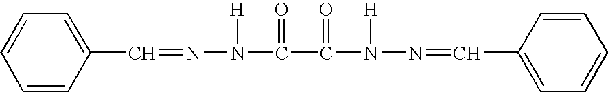
are introduced into 800 mass parts of dimethylformamide and dissolved by heating. Both solutions are then mixed and reacted. Immediately afterward, before the solution cools and the resulting palladium complex precipitates out, support particles, which are composed of a pyrogenic silicic acid which is obtainable under the name “Aerosil 200,”are soaked in the solution. After a drying and grinding process, the support particles are mixed in accordance with a conventional preparatory process into a batch of polymer powder in a proportion of up to 50%. After the material has been agglomerated in a hot mixer, it is granulated in a granulator. The synthetic resin granules now contain the necessary amount of the organic heavy metal complex in the pore structure of the incorporated support particles. The granules are then processed by injection molding to form three-dimensional circuit supports.
The circuit supports are then irradiated through a mask with excimer laser ultraviolet radiation having a wavelength of 248 mm. In the irradiated areas the support particles are thus exposed by ablation of the surrounding polymer matrix and at the same time very finely divided metallic palladium is cleaved out of the heavy metal complex in and around the pores of the support particles. In a conventional commercial reductive copper bath without an external power supply, copper deposits itself selectively in the irradiated areas in a very firmly adherent manner. The conductor tracks are formed, and a ready-to-use circuit support is produced.
Alternatively, it is also possible to use Aerogels as support particles. The highly porous solids of SiO2 with a BET surface area of up to 1000 m2/g permit a still stronger bonding of the metal conductor tracks to the circuit supports.
Claims (29)
1. A conductor track structure on an area of a nonconductive support material, said conductor track structure comprising a palladium containing base and a metallized layer applied to said base, said palladium containing base comprising palladium containing nuclei formed by breaking up a non-conductive organic palladium containing complex in said area of said nonconductive support material, and said support material containing microporous or microrough support particles to which said palladium containing nuclei are bound, wherein said support particles are selected from the group consisting of pyrogenic silicic acid and aerogels.
2. A conductor track structure according to claim 1 , wherein said support material comprises a polymer matrix having said support particles embedded therein.
3. A conductor track structure according to claim 1 , wherein said support material comprises a polymer matrix having said support particles bound thereto.
4. A conductor track structure according to claim 1 , wherein said support particles are formed of pyrogenic silicic acid having a BET surface area of 200 m2/g.
5. A conductor track structure according to claim 1 , wherein said support particles are formed of aerogels.
6. A method of producing a conductor track structure on an area of a nonconductive support material, said conductor track structure comprising a palladium containing base and a metallized layer applied to said base, wherein said area of said nonconductive support material comprises microporous or microrough support particles having a nonconductive palladium containing organic complex bound thereto; and said method comprises the steps of:
selectively applying electromagnetic radiation in the ultraviolet range to said area of said nonconductive support material to expose said support particles by ablation and break down said palladium containing organic complex to release palladium containing nuclei in said area, and
thereafter metallizing said area by chemical reduction.
7. A method according to claim 6 , wherein said support particles are mixed into and embedded within said support material.
8. A method according to claim 6 , wherein said support particles are mixed into a coating material applied to a surface of the support material.
9. A method according to claim 6 , wherein an ultraviolet laser, an excimer laser or an ultraviolet radiator is used as a source of said selectively applied electromagnetic radiation.
10. A method according to claim 6 , wherein the source of said selectively applied electromagnetic radiation is a KrF excimer laser with a wavelength of 248 nm.
11. A method according to claim 6 , wherein said support particles are resistant to ultraviolet radiation.
12. A method according to claim 6 , wherein said palladium containing organic complex is bound to said support particles by immersing the particles in a solution of the palladium containing complex and then drying the resulting particles.
13. A method according to claim 6 , wherein the support particles with the palladium containing complex bound thereto are mixed into coating material and then applied as coating to the support material.
14. A method according to claim 6 , wherein said support particles are inorganic mineral particles.
15. A method according to claim 14 , wherein said support particles are formed of pyrogenic silicic acid or of aerogels.
16. A method according to claim 14 , wherein said support particles are formed of pyrogenic silicic acid with a BET surface area of 200 m2/g.
17. A method according to claim 6 , wherein said palladium containing organic complex is a palladium complex formed by reacting a palladium salt with an organic complexing agent, and precipitating the resulting palladium complex.
18. A method according to claim 17 , wherein said palladium salt is palladium diacetate, and said organic complexing agent is a stable, polyfunctional chelating agent.
19. A method according to claim 18 , wherein said chelating agent comprises a plurality of ligand atoms selected from the group consisting of nitrogen, oxygen, sulfur and phosphorus.
20. A method according to claim 18 , wherein said chelating agent comprises ionizing groups selected from the group consisting of hydroxyl and carboxyl groups.
21. A method according to claim 17 , wherein said organic complexing agent is a molecular combination of sterically hindered aromatic groups and metal-complexing groups.
22. A method according to claim 21 , wherein said organic completing agent is a compound corresponding to the formula: 
23. A method of producing a conductor track structure on an area of a nonconductive support material, said conductor track structure comprising a palladium containing base and a metallized layer applied to said base, wherein said area of said nonconductive support material comprises microporous or microrough support particles having a nonconductive paladium containing organic complex bound thereto;
and said method comprises:
selectively applying electromagnetic radiation from an ultraviolet laser, an excimer laser or an ultraviolet radiator to said area of said nonconductive support material to expose said support particles by ablation and break down said palladium containing organic complex to release palladium containing nuclei in said area, and
thereafter metallizing said area by chemical reduction.
24. A method according to claim 23 , wherein said support particles are mixed into and embedded within said support material.
25. A method according to claim 23 , wherein said support particles are mixed into a coating material applied to a surface of the support material.
26. A method according to claim 23 , wherein said support particles are resistant to ultraviolet radiation.
27. A method according to claim 23 , wherein said support particles are inorganic mineral particles.
28. A method according to claim 23 , wherein said palladium containing organic complex is bound to said support particles by immersing the particles in a solution of the palladium containing complex and then drying the resulting particles.
29. A method according to claim 23 , the support particles with the palladium containing complex bound thereto are mixed into coating material and then applied as coating to the support material.
Applications Claiming Priority (3)
| Application Number | Priority Date | Filing Date | Title |
|---|---|---|---|
| DE19731346 | 1997-07-22 | ||
| DE1997131346 DE19731346C2 (en) | 1997-06-06 | 1997-07-22 | Conductor structures and a method for their production |
| PCT/EP1998/004413 WO1999005895A1 (en) | 1997-07-22 | 1998-07-16 | Conducting path structures situated on a non-conductive support material, especially fine conducting path structures and method for producing same |
Publications (1)
| Publication Number | Publication Date |
|---|---|
| US6696173B1 true US6696173B1 (en) | 2004-02-24 |
Family
ID=7836451
Family Applications (1)
| Application Number | Title | Priority Date | Filing Date |
|---|---|---|---|
| US09/254,953 Expired - Lifetime US6696173B1 (en) | 1997-07-22 | 1998-07-16 | Conducting path structures situated on a non-conductive support material, especially fine conducting path structures and method for producing same |
Country Status (8)
| Country | Link |
|---|---|
| US (1) | US6696173B1 (en) |
| EP (1) | EP0927507B1 (en) |
| JP (1) | JP3366652B2 (en) |
| KR (1) | KR100374667B1 (en) |
| CN (1) | CN1234960A (en) |
| AT (1) | ATE369726T1 (en) |
| DE (2) | DE19731346C2 (en) |
| WO (1) | WO1999005895A1 (en) |
Cited By (80)
| Publication number | Priority date | Publication date | Assignee | Title |
|---|---|---|---|---|
| US20040241422A1 (en) * | 2001-07-05 | 2004-12-02 | Lpkf Laser & Electronics Ag | Conductor track structures and method for production thereof |
| US20050100130A1 (en) * | 2000-04-06 | 2005-05-12 | Hamamatsu Photonics K.K. | X-ray inspection system |
| US20050224092A1 (en) * | 2004-04-08 | 2005-10-13 | Enthone Inc. | Method for treating laser-structured plastic surfaces |
| US20060083939A1 (en) * | 2004-10-20 | 2006-04-20 | Dunbar Meredith L | Light activatable polyimide compositions for receiving selective metalization, and methods and compositions related thereto |
| US20060275705A1 (en) * | 2005-06-01 | 2006-12-07 | Hewlett-Packard Development Company Lp | Conductive patterning |
| US20090043191A1 (en) * | 2007-07-12 | 2009-02-12 | Volcano Corporation | Oct-ivus catheter for concurrent luminal imaging |
| US20090163045A1 (en) * | 2007-12-21 | 2009-06-25 | Molex Incorporated | Plated dielectric frame with integrated connector |
| US20090263639A1 (en) * | 2004-10-20 | 2009-10-22 | E. I. Du Pont De Nemours And Company | Light activatable polyimide compositions for receiving selective metalization, and methods and compositions related thereto |
| US20100009173A1 (en) * | 2007-07-09 | 2010-01-14 | E. I. Du Ponte De Nemours And Company | Compositions and methods for creating electronic circuitry |
| DE112008001425T5 (en) | 2007-05-25 | 2010-04-15 | Molex Inc., Lisle | A connection device that forms a heat sink and electrical connections between a heat generating device and a power source |
| US20110212345A1 (en) * | 2010-01-15 | 2011-09-01 | Byd Company Limited | Metalized plastic articles and methods thereof |
| US20110212344A1 (en) * | 2010-02-26 | 2011-09-01 | Qing Gong | Metalized Plastic Articles and Methods Thereof |
| EP2379772A1 (en) * | 2009-12-17 | 2011-10-26 | BYD Company Limited | Surface metallizing method, method for preparing plastic article and plastic article made therefrom |
| EP2397512A1 (en) * | 2010-06-17 | 2011-12-21 | Dr. Schneider Kunststoffwerke GmbH | Plastic section for use in the interior of a motor vehicle |
| EP2476723A1 (en) * | 2011-01-14 | 2012-07-18 | LPKF Laser & Electronics AG | Method for selective metallisation of a substrate and switch holder produced according to this method |
| CN102978593A (en) * | 2009-12-17 | 2013-03-20 | 比亚迪股份有限公司 | Method for selectively metalizing surface of plastic |
| US8841000B2 (en) | 2010-08-19 | 2014-09-23 | Byd Company Limited | Metalized plastic articles and methods thereof |
| US9074070B2 (en) | 2011-10-31 | 2015-07-07 | Ticona Llc | Thermoplastic composition for use in forming a laser direct structured substrate |
| KR20150077609A (en) | 2013-12-28 | 2015-07-08 | 전자부품연구원 | Hybrid Composite materials capable of fabrication of selective conducting pattern by Laser for 3D printing, manufacturing method of 3D electronic devices with the selective conducting pattern and 3D electronic devices thereby |
| US9226711B2 (en) | 2012-12-21 | 2016-01-05 | Volcano Corporation | Laser direct structured catheter connection for intravascular device |
| US9286673B2 (en) | 2012-10-05 | 2016-03-15 | Volcano Corporation | Systems for correcting distortions in a medical image and methods of use thereof |
| US9292918B2 (en) | 2012-10-05 | 2016-03-22 | Volcano Corporation | Methods and systems for transforming luminal images |
| US9295162B2 (en) | 2010-03-12 | 2016-03-22 | Taiwan Green Point Enterprises Co., Ltd. | Non-deleterious technique for creating continuous conductive circuits upon the surfaces of a non-conductive substrate |
| US9301687B2 (en) | 2013-03-13 | 2016-04-05 | Volcano Corporation | System and method for OCT depth calibration |
| US9307926B2 (en) | 2012-10-05 | 2016-04-12 | Volcano Corporation | Automatic stent detection |
| US9324141B2 (en) | 2012-10-05 | 2016-04-26 | Volcano Corporation | Removal of A-scan streaking artifact |
| US9360630B2 (en) | 2011-08-31 | 2016-06-07 | Volcano Corporation | Optical-electrical rotary joint and methods of use |
| US9367965B2 (en) | 2012-10-05 | 2016-06-14 | Volcano Corporation | Systems and methods for generating images of tissue |
| US9383263B2 (en) | 2012-12-21 | 2016-07-05 | Volcano Corporation | Systems and methods for narrowing a wavelength emission of light |
| US9398703B2 (en) | 2014-05-19 | 2016-07-19 | Sierra Circuits, Inc. | Via in a printed circuit board |
| US9474161B2 (en) | 2010-03-12 | 2016-10-18 | Taiwan Green Point Enterprises Co., Ltd. | Circuit substrate having a circuit pattern and method for making the same |
| US9478940B2 (en) | 2012-10-05 | 2016-10-25 | Volcano Corporation | Systems and methods for amplifying light |
| US9486143B2 (en) | 2012-12-21 | 2016-11-08 | Volcano Corporation | Intravascular forward imaging device |
| US9587316B2 (en) | 2012-09-14 | 2017-03-07 | Mitsubishi Engineering-Plastics Corporation | Thermoplastic resin composition, resin molded article, and method for manufacturing resin molded article having a plated layer |
| US9590292B2 (en) | 2014-12-08 | 2017-03-07 | Industrial Technology Research Institute | Beam antenna |
| US9596993B2 (en) | 2007-07-12 | 2017-03-21 | Volcano Corporation | Automatic calibration systems and methods of use |
| US9612105B2 (en) | 2012-12-21 | 2017-04-04 | Volcano Corporation | Polarization sensitive optical coherence tomography system |
| US9622706B2 (en) | 2007-07-12 | 2017-04-18 | Volcano Corporation | Catheter for in vivo imaging |
| US9678532B2 (en) | 2010-03-12 | 2017-06-13 | Taiwan Green Point Enterprises Co., Ltd. | Capacitive touch sensitive housing and method for making the same |
| US9706650B1 (en) | 2016-08-18 | 2017-07-11 | Sierra Circuits, Inc. | Catalytic laminate apparatus and method |
| US9709379B2 (en) | 2012-12-20 | 2017-07-18 | Volcano Corporation | Optical coherence tomography system that is reconfigurable between different imaging modes |
| US9730613B2 (en) | 2012-12-20 | 2017-08-15 | Volcano Corporation | Locating intravascular images |
| US9770172B2 (en) | 2013-03-07 | 2017-09-26 | Volcano Corporation | Multimodal segmentation in intravascular images |
| US9858668B2 (en) | 2012-10-05 | 2018-01-02 | Volcano Corporation | Guidewire artifact removal in images |
| US9867530B2 (en) | 2006-08-14 | 2018-01-16 | Volcano Corporation | Telescopic side port catheter device with imaging system and method for accessing side branch occlusions |
| US9896566B2 (en) | 2014-07-01 | 2018-02-20 | Ticona Llc | Laser activatable polymer composition |
| US10058284B2 (en) | 2012-12-21 | 2018-08-28 | Volcano Corporation | Simultaneous imaging, monitoring, and therapy |
| US10070827B2 (en) | 2012-10-05 | 2018-09-11 | Volcano Corporation | Automatic image playback |
| US10148006B2 (en) | 2012-09-14 | 2018-12-04 | Mitsubishi Engineering-Plastics Corporation | Thermoplastic resin composition, resin molded article, and method for manufacturing resin molded article having a plated layer |
| US10166003B2 (en) | 2012-12-21 | 2019-01-01 | Volcano Corporation | Ultrasound imaging with variable line density |
| US10191220B2 (en) | 2012-12-21 | 2019-01-29 | Volcano Corporation | Power-efficient optical circuit |
| US10219887B2 (en) | 2013-03-14 | 2019-03-05 | Volcano Corporation | Filters with echogenic characteristics |
| US10226597B2 (en) | 2013-03-07 | 2019-03-12 | Volcano Corporation | Guidewire with centering mechanism |
| US10238367B2 (en) | 2012-12-13 | 2019-03-26 | Volcano Corporation | Devices, systems, and methods for targeted cannulation |
| US10292677B2 (en) | 2013-03-14 | 2019-05-21 | Volcano Corporation | Endoluminal filter having enhanced echogenic properties |
| US10332228B2 (en) | 2012-12-21 | 2019-06-25 | Volcano Corporation | System and method for graphical processing of medical data |
| US10349520B2 (en) | 2017-06-28 | 2019-07-09 | Catlam, Llc | Multi-layer circuit board using interposer layer and conductive paste |
| US10413317B2 (en) | 2012-12-21 | 2019-09-17 | Volcano Corporation | System and method for catheter steering and operation |
| US10420530B2 (en) | 2012-12-21 | 2019-09-24 | Volcano Corporation | System and method for multipath processing of image signals |
| US10426590B2 (en) | 2013-03-14 | 2019-10-01 | Volcano Corporation | Filters with echogenic characteristics |
| US10568586B2 (en) | 2012-10-05 | 2020-02-25 | Volcano Corporation | Systems for indicating parameters in an imaging data set and methods of use |
| US10574232B2 (en) | 2016-09-26 | 2020-02-25 | Hyundai Motor Company | Control apparatus using dial, manufacturing method of control apparatus using dial and vehicle including the same |
| US10595820B2 (en) | 2012-12-20 | 2020-03-24 | Philips Image Guided Therapy Corporation | Smooth transition catheters |
| US10638939B2 (en) | 2013-03-12 | 2020-05-05 | Philips Image Guided Therapy Corporation | Systems and methods for diagnosing coronary microvascular disease |
| US10685931B2 (en) | 2016-11-12 | 2020-06-16 | Catlam Llc | Method and apparatus for forming contacts on an integrated circuit die using a catalytic adhesive |
| US10724082B2 (en) | 2012-10-22 | 2020-07-28 | Bio-Rad Laboratories, Inc. | Methods for analyzing DNA |
| US10765012B2 (en) | 2017-07-10 | 2020-09-01 | Catlam, Llc | Process for printed circuit boards using backing foil |
| US10758207B2 (en) | 2013-03-13 | 2020-09-01 | Philips Image Guided Therapy Corporation | Systems and methods for producing an image from a rotational intravascular ultrasound device |
| US10827624B2 (en) | 2018-03-05 | 2020-11-03 | Catlam, Llc | Catalytic laminate with conductive traces formed during lamination |
| US10837114B2 (en) | 2014-10-23 | 2020-11-17 | Lg Chem., Ltd. | Composition for forming conductive pattern by irradiation of electromagnetic waves, method for forming conductive pattern using same, and resin structure having conductive pattern |
| US10849233B2 (en) | 2017-07-10 | 2020-11-24 | Catlam, Llc | Process for forming traces on a catalytic laminate |
| US10942022B2 (en) | 2012-12-20 | 2021-03-09 | Philips Image Guided Therapy Corporation | Manual calibration of imaging system |
| US10939826B2 (en) | 2012-12-20 | 2021-03-09 | Philips Image Guided Therapy Corporation | Aspirating and removing biological material |
| US10993694B2 (en) | 2012-12-21 | 2021-05-04 | Philips Image Guided Therapy Corporation | Rotational ultrasound imaging catheter with extended catheter body telescope |
| US11026591B2 (en) | 2013-03-13 | 2021-06-08 | Philips Image Guided Therapy Corporation | Intravascular pressure sensor calibration |
| US11040140B2 (en) | 2010-12-31 | 2021-06-22 | Philips Image Guided Therapy Corporation | Deep vein thrombosis therapeutic methods |
| US11141063B2 (en) | 2010-12-23 | 2021-10-12 | Philips Image Guided Therapy Corporation | Integrated system architectures and methods of use |
| US11154313B2 (en) | 2013-03-12 | 2021-10-26 | The Volcano Corporation | Vibrating guidewire torquer and methods of use |
| US11272845B2 (en) | 2012-10-05 | 2022-03-15 | Philips Image Guided Therapy Corporation | System and method for instant and automatic border detection |
| US11406498B2 (en) | 2012-12-20 | 2022-08-09 | Philips Image Guided Therapy Corporation | Implant delivery system and implants |
Families Citing this family (44)
| Publication number | Priority date | Publication date | Assignee | Title |
|---|---|---|---|---|
| US6284563B1 (en) | 1995-10-31 | 2001-09-04 | Tessera, Inc. | Method of making compliant microelectronic assemblies |
| DE59914360D1 (en) * | 1998-12-10 | 2007-07-12 | Lpkf Laser & Electronics Ag | METHOD FOR PRODUCING LINEAR STRUCTURES |
| DE19927749A1 (en) | 1999-06-17 | 2000-12-28 | Siemens Ag | Electronic arrangement used as a semiconductor chip has electrical contacts on a first surface with a flexible elevation made of an insulating material |
| EP1186035A1 (en) | 1999-06-17 | 2002-03-13 | Infineon Technologies AG | Electronic component with flexible contact structures and method for the production of said component |
| DE19943385B4 (en) | 1999-09-10 | 2006-06-14 | Infineon Technologies Ag | Method for making an electrical connection between the front and back of semiconductor chips |
| DE10016132A1 (en) | 2000-03-31 | 2001-10-18 | Infineon Technologies Ag | Electronic component for electronic devices comprises electronic switch and conducting paths on surface of the component to electrically connect the switch with metal-coated protrusions made from rubber-elastic insulating material |
| DE10125570B4 (en) * | 2001-05-25 | 2008-09-25 | Ticona Gmbh | Method for connecting printed conductors to plastic surfaces |
| JP3881338B2 (en) * | 2001-07-05 | 2007-02-14 | エル・ピー・ケー・エフ・レーザー・ウント・エレクトロニクス・アクチエンゲゼルシヤフト | Conductor track structure and manufacturing method thereof |
| DE102004052301A1 (en) * | 2004-10-27 | 2006-05-11 | Jens Freye | Production of strip conductors for circuit boards comprises forming the strip conductors using a energy beam or energy pulse and reinforcing by metallizing |
| DE102004052303A1 (en) * | 2004-10-27 | 2006-05-11 | Jens Freye | Producing functional element structures, especially circuit boards, e.g. for use in mobile telephones, using energy radiation or energy pulses, specifically for chemical conversion of compound in substrate material |
| DE102004052300A1 (en) * | 2004-10-27 | 2006-05-11 | Jens Freye | Production of conductor strip structures, especially for conductor plate for PCB by use of energy beam or energy pulses useful in metallizing and in mobile phones |
| DE102006017630A1 (en) * | 2006-04-12 | 2007-10-18 | Lpkf Laser & Electronics Ag | Method for producing a printed conductor structure and a printed conductor structure produced in this way |
| KR100712346B1 (en) | 2006-06-30 | 2007-05-02 | 주식회사 이엠따블유안테나 | Antenna with 3-d configuration |
| KR101309332B1 (en) | 2006-08-17 | 2013-09-16 | 주식회사 이엠따블유 | Method of forming antenna pattern on plastic molding and plastic molding comprising antenna pattern produced thereby |
| DE102006053982B4 (en) * | 2006-11-10 | 2009-10-29 | Infineon Technologies Ag | Three dimensional carrier structure i.e. molded interconnect device, for electronic or optoelectronic assembly, has metal coating representing electromagnetic screening structure together with metal seed layer formed in carrier material |
| US9173047B2 (en) | 2008-09-18 | 2015-10-27 | Fujifilm Sonosite, Inc. | Methods for manufacturing ultrasound transducers and other components |
| CN103811366B (en) * | 2008-09-18 | 2017-04-12 | 富士胶卷视声公司 | Methods For Manufacturing Ultrasound Transducers And Other Components |
| US9184369B2 (en) | 2008-09-18 | 2015-11-10 | Fujifilm Sonosite, Inc. | Methods for manufacturing ultrasound transducers and other components |
| ATE522568T1 (en) | 2009-03-27 | 2011-09-15 | Lanxess Deutschland Gmbh | HOT WIRE RESISTANT POLYESTER |
| FR2965822A1 (en) * | 2010-10-07 | 2012-04-13 | Valeo Securite Habitacle | Fabricating and decorating automobile trim part e.g. door handle comprising non-conductive material, comprises integrating non-conductive heavy metal complex in non-conductive material, and multi-injection molding trim part with complexes |
| DE102010052033A1 (en) * | 2010-11-23 | 2012-05-24 | Leibniz-Institut Für Neue Materialien Gemeinnützige Gmbh | Process for the production of metallic structures |
| WO2012128219A1 (en) | 2011-03-18 | 2012-09-27 | ミツビシ ケミカル ヨーロッパ ゲーエムベーハー | Thermoplastic resin composition, resin molding, and process for producing resin molding having plating layer attached thereto |
| DE102011007537A1 (en) | 2011-04-15 | 2012-10-18 | Fraunhofer-Gesellschaft zur Förderung der angewandten Forschung e.V. | In a plastic body embedded functional element and method for electrically contacting a embedded in a plastic body functional element |
| US9365693B2 (en) | 2012-03-23 | 2016-06-14 | Mitsubishi Engineering-Plastics Corporation | Thermoplastic resin composition, resin article, and method of manufacturing resin article with plated layer |
| US9374650B2 (en) | 2012-07-17 | 2016-06-21 | Starkey Laboratories, Inc. | System and method for embedding conductive traces into hearing assistance device housings |
| CN104583331A (en) | 2012-09-14 | 2015-04-29 | 三菱工程塑料株式会社 | Thermoplastic resin composition, resin molded article, and method for producing resin molded article having plated layer attached thereto |
| US20160215124A1 (en) | 2013-09-05 | 2016-07-28 | Mitsubishi Engineering-Plastics Corporation | Thermoplastic resin composition, resin molded article, and method for manufacturing the resin molded article with plating layer |
| US20160298242A1 (en) | 2013-11-18 | 2016-10-13 | Mitsubishi Engineering-Plastics Corporation | Processes for manufacturing resin molded articles |
| KR101584246B1 (en) | 2014-10-17 | 2016-01-11 | 에스케이씨 주식회사 | Conductive pattern structure and preparation method thereof |
| CN105813371B (en) * | 2014-12-31 | 2019-12-10 | 比亚迪股份有限公司 | Circuit board, preparation method and application thereof, and micro-projector module |
| KR101762331B1 (en) | 2015-06-10 | 2017-07-27 | 에스케이씨 주식회사 | Conductive pattern structure and preparation method thereof |
| US10203799B2 (en) | 2015-09-15 | 2019-02-12 | Hyundai Motor Company | Touch input device, vehicle comprising touch input device, and manufacturing method of touch input device |
| US20170075473A1 (en) | 2015-09-15 | 2017-03-16 | Hyundai Motor Company | Touch input device and method for manufacturing the same |
| KR20170058742A (en) | 2015-11-19 | 2017-05-29 | 현대자동차주식회사 | Touch control device, vehicle comprising the same, and manufacturing method thereof |
| KR101741654B1 (en) | 2015-11-19 | 2017-05-30 | 현대자동차주식회사 | Touch control device, vehicle comprising the same, and manufacturing method thereof |
| KR101728329B1 (en) | 2015-11-19 | 2017-05-02 | 현대자동차주식회사 | Touch control device, vehicle comprising the same, and manufacturing method thereof |
| DE102016202589A1 (en) | 2016-02-19 | 2017-08-24 | Continental Automotive Gmbh | Method for electrically connecting components for a motor vehicle and device for a motor vehicle |
| EP3387887A1 (en) | 2015-12-11 | 2018-10-17 | Continental Automotive GmbH | Method for sealing and/or electrically connecting components for a motor vehicle, and device for a motor vehicle |
| KR101795540B1 (en) * | 2016-07-04 | 2017-11-10 | 현대자동차주식회사 | Touch controll device |
| KR101851146B1 (en) | 2016-09-21 | 2018-04-24 | 현대자동차주식회사 | Camera for vehicle |
| KR101866736B1 (en) | 2016-09-23 | 2018-06-15 | 현대자동차주식회사 | Touch controll device and manufacturing method thereof |
| WO2019167854A1 (en) | 2018-02-27 | 2019-09-06 | 三菱エンジニアリングプラスチックス株式会社 | Thermoplastic resin composition, molded article, method for manufacturing thermoplastic resin composition, and method for manufacturing plated molded article |
| DK3554096T3 (en) | 2018-04-11 | 2023-06-19 | Gn Hearing As | HEARING AID HOUSING WITH INTEGRATED ANTENNA |
| WO2021090824A1 (en) | 2019-11-06 | 2021-05-14 | 三菱エンジニアリングプラスチックス株式会社 | Resin composition for laser direct structuring, molded product, and production method of plated molded product |
Citations (16)
| Publication number | Priority date | Publication date | Assignee | Title |
|---|---|---|---|---|
| US3546011A (en) * | 1967-04-12 | 1970-12-08 | Degussa | Process for the production of electricity conducting surfaces on a nonconducting support |
| US4133929A (en) * | 1976-06-24 | 1979-01-09 | Ciba-Geigy Corporation | Ionically modified cellulose materials for removal of heavy metal ions |
| US4169082A (en) * | 1978-03-31 | 1979-09-25 | Johns-Manville Corporation | Flame resistant low-smoke hot melt adhesive |
| US4251596A (en) * | 1977-10-28 | 1981-02-17 | Bayer Aktiengesellschaft | Production of non-stick coatings |
| US4504529A (en) * | 1979-04-11 | 1985-03-12 | A/S Neselco | Xerographic method for dry sensitization and electroless coating of an insulating surface and a powder for use with the method |
| JPS61141774A (en) * | 1984-12-13 | 1986-06-28 | Sumitomo Bakelite Co Ltd | Adhesive for additive plating |
| US4668330A (en) * | 1985-12-05 | 1987-05-26 | Monsanto Company | Furnace contamination |
| US4692345A (en) * | 1983-12-01 | 1987-09-08 | Fuji Electric Corporate Research And Devel., Ltd. | Method for gettering heavy metal from a silicon plate |
| US4726908A (en) * | 1985-02-11 | 1988-02-23 | Henkel Kommanditgesellschaft Auf Aktien | Agglomeration process including a heating step for making a free-flowing granulate |
| EP0277325A1 (en) * | 1986-12-17 | 1988-08-10 | Siemens Aktiengesellschaft | Method of and coating material for producing a printed conductive pattern on an insulated substrate |
| US5032488A (en) * | 1985-08-23 | 1991-07-16 | Ciba-Geigy Corporation | Method of metalizing a surface using a mixture of olefin and dibenzalacetone palladium complex |
| JPH0537129A (en) * | 1991-07-31 | 1993-02-12 | Hitachi Aic Inc | Manufacture of printed wiring board |
| US5405656A (en) * | 1990-04-02 | 1995-04-11 | Nippondenso Co., Ltd. | Solution for catalytic treatment, method of applying catalyst to substrate and method of forming electrical conductor |
| US5487964A (en) * | 1993-06-15 | 1996-01-30 | Bayer Aktiengesellschaft | Powder mixtures for metallization of substrate surfaces |
| US5593739A (en) * | 1995-02-14 | 1997-01-14 | Lpkf Cad/Cam Systeme Gmbh | Method of patterned metallization of substrate surfaces |
| US6319564B1 (en) * | 1997-06-06 | 2001-11-20 | Gerhard Naundorf | Conductor track structures arranged on a nonconductive support material, especially fine conductor track structures, and method for producing the same |
Family Cites Families (1)
| Publication number | Priority date | Publication date | Assignee | Title |
|---|---|---|---|---|
| DE4042220C2 (en) * | 1990-12-29 | 1995-02-02 | Heraeus Noblelight Gmbh | Process for the production of all-over or partial gold layers |
-
1997
- 1997-07-22 DE DE1997131346 patent/DE19731346C2/en not_active Expired - Fee Related
-
1998
- 1998-07-16 CN CN98801024A patent/CN1234960A/en active Pending
- 1998-07-16 JP JP50926799A patent/JP3366652B2/en not_active Expired - Fee Related
- 1998-07-16 KR KR10-1999-7002375A patent/KR100374667B1/en not_active IP Right Cessation
- 1998-07-16 DE DE59814073T patent/DE59814073D1/en not_active Expired - Lifetime
- 1998-07-16 US US09/254,953 patent/US6696173B1/en not_active Expired - Lifetime
- 1998-07-16 AT AT98942560T patent/ATE369726T1/en not_active IP Right Cessation
- 1998-07-16 WO PCT/EP1998/004413 patent/WO1999005895A1/en active IP Right Grant
- 1998-07-16 EP EP98942560A patent/EP0927507B1/en not_active Expired - Lifetime
Patent Citations (16)
| Publication number | Priority date | Publication date | Assignee | Title |
|---|---|---|---|---|
| US3546011A (en) * | 1967-04-12 | 1970-12-08 | Degussa | Process for the production of electricity conducting surfaces on a nonconducting support |
| US4133929A (en) * | 1976-06-24 | 1979-01-09 | Ciba-Geigy Corporation | Ionically modified cellulose materials for removal of heavy metal ions |
| US4251596A (en) * | 1977-10-28 | 1981-02-17 | Bayer Aktiengesellschaft | Production of non-stick coatings |
| US4169082A (en) * | 1978-03-31 | 1979-09-25 | Johns-Manville Corporation | Flame resistant low-smoke hot melt adhesive |
| US4504529A (en) * | 1979-04-11 | 1985-03-12 | A/S Neselco | Xerographic method for dry sensitization and electroless coating of an insulating surface and a powder for use with the method |
| US4692345A (en) * | 1983-12-01 | 1987-09-08 | Fuji Electric Corporate Research And Devel., Ltd. | Method for gettering heavy metal from a silicon plate |
| JPS61141774A (en) * | 1984-12-13 | 1986-06-28 | Sumitomo Bakelite Co Ltd | Adhesive for additive plating |
| US4726908A (en) * | 1985-02-11 | 1988-02-23 | Henkel Kommanditgesellschaft Auf Aktien | Agglomeration process including a heating step for making a free-flowing granulate |
| US5032488A (en) * | 1985-08-23 | 1991-07-16 | Ciba-Geigy Corporation | Method of metalizing a surface using a mixture of olefin and dibenzalacetone palladium complex |
| US4668330A (en) * | 1985-12-05 | 1987-05-26 | Monsanto Company | Furnace contamination |
| EP0277325A1 (en) * | 1986-12-17 | 1988-08-10 | Siemens Aktiengesellschaft | Method of and coating material for producing a printed conductive pattern on an insulated substrate |
| US5405656A (en) * | 1990-04-02 | 1995-04-11 | Nippondenso Co., Ltd. | Solution for catalytic treatment, method of applying catalyst to substrate and method of forming electrical conductor |
| JPH0537129A (en) * | 1991-07-31 | 1993-02-12 | Hitachi Aic Inc | Manufacture of printed wiring board |
| US5487964A (en) * | 1993-06-15 | 1996-01-30 | Bayer Aktiengesellschaft | Powder mixtures for metallization of substrate surfaces |
| US5593739A (en) * | 1995-02-14 | 1997-01-14 | Lpkf Cad/Cam Systeme Gmbh | Method of patterned metallization of substrate surfaces |
| US6319564B1 (en) * | 1997-06-06 | 2001-11-20 | Gerhard Naundorf | Conductor track structures arranged on a nonconductive support material, especially fine conductor track structures, and method for producing the same |
Non-Patent Citations (2)
| Title |
|---|
| G.G. Hawley, Condensed Chemical Dictionary, 9th edition, 1977 (New York), Van Nostrand Reinhold Co., p. 430 (no month).* * |
| J. Ganz et al., "LAD-Ein neuartiges lasergestutztes Beschichtungsverfahren fur Feinstleitermetallisierungen," GALVANOTECHNIK., Bd. 81, Nr. 10, Oktober 1990, Seiten 3661-3668, XP002085825, (Oct. 1990). * |
Cited By (117)
| Publication number | Priority date | Publication date | Assignee | Title |
|---|---|---|---|---|
| US20050100130A1 (en) * | 2000-04-06 | 2005-05-12 | Hamamatsu Photonics K.K. | X-ray inspection system |
| US7060421B2 (en) * | 2001-07-05 | 2006-06-13 | Lpkf Laser & Electronics Ag | Conductor track structures and method for production thereof |
| US20040241422A1 (en) * | 2001-07-05 | 2004-12-02 | Lpkf Laser & Electronics Ag | Conductor track structures and method for production thereof |
| US20050224092A1 (en) * | 2004-04-08 | 2005-10-13 | Enthone Inc. | Method for treating laser-structured plastic surfaces |
| US7578888B2 (en) | 2004-04-08 | 2009-08-25 | Enthone Inc. | Method for treating laser-structured plastic surfaces |
| US20090263639A1 (en) * | 2004-10-20 | 2009-10-22 | E. I. Du Pont De Nemours And Company | Light activatable polyimide compositions for receiving selective metalization, and methods and compositions related thereto |
| US20060083939A1 (en) * | 2004-10-20 | 2006-04-20 | Dunbar Meredith L | Light activatable polyimide compositions for receiving selective metalization, and methods and compositions related thereto |
| US8323802B2 (en) | 2004-10-20 | 2012-12-04 | E I Du Pont De Nemours And Company | Light activatable polyimide compositions for receiving selective metalization, and methods and compositions related thereto |
| US20060275705A1 (en) * | 2005-06-01 | 2006-12-07 | Hewlett-Packard Development Company Lp | Conductive patterning |
| WO2006130582A1 (en) * | 2005-06-01 | 2006-12-07 | Hewlett-Packard Development Company, L.P. | Conductive patterning |
| US7569331B2 (en) | 2005-06-01 | 2009-08-04 | Hewlett-Packard Development Company, L.P. | Conductive patterning |
| US9867530B2 (en) | 2006-08-14 | 2018-01-16 | Volcano Corporation | Telescopic side port catheter device with imaging system and method for accessing side branch occlusions |
| DE112008001425T5 (en) | 2007-05-25 | 2010-04-15 | Molex Inc., Lisle | A connection device that forms a heat sink and electrical connections between a heat generating device and a power source |
| US20100009173A1 (en) * | 2007-07-09 | 2010-01-14 | E. I. Du Ponte De Nemours And Company | Compositions and methods for creating electronic circuitry |
| US8475924B2 (en) | 2007-07-09 | 2013-07-02 | E.I. Du Pont De Nemours And Company | Compositions and methods for creating electronic circuitry |
| US8449949B2 (en) | 2007-07-09 | 2013-05-28 | E. I. Du Pont De Nemours And Company | Compositions and methods for creating electronic circuitry |
| US9596993B2 (en) | 2007-07-12 | 2017-03-21 | Volcano Corporation | Automatic calibration systems and methods of use |
| US20090043191A1 (en) * | 2007-07-12 | 2009-02-12 | Volcano Corporation | Oct-ivus catheter for concurrent luminal imaging |
| US10219780B2 (en) | 2007-07-12 | 2019-03-05 | Volcano Corporation | OCT-IVUS catheter for concurrent luminal imaging |
| US9622706B2 (en) | 2007-07-12 | 2017-04-18 | Volcano Corporation | Catheter for in vivo imaging |
| US11350906B2 (en) | 2007-07-12 | 2022-06-07 | Philips Image Guided Therapy Corporation | OCT-IVUS catheter for concurrent luminal imaging |
| US20090163045A1 (en) * | 2007-12-21 | 2009-06-25 | Molex Incorporated | Plated dielectric frame with integrated connector |
| US7815475B2 (en) * | 2007-12-21 | 2010-10-19 | Molex Incorporated | Three-dimensional plated support frame |
| CN102978593B (en) * | 2009-12-17 | 2015-07-22 | 比亚迪股份有限公司 | Method for selectively metalizing surface of plastic |
| CN102978593A (en) * | 2009-12-17 | 2013-03-20 | 比亚迪股份有限公司 | Method for selectively metalizing surface of plastic |
| EP2584064A3 (en) * | 2009-12-17 | 2013-05-01 | BYD Company Limited | Surface metallizing method, method for preparing plastic article and plastic article made therefrom |
| EP2584066A3 (en) * | 2009-12-17 | 2013-05-01 | BYD Company Limited | Surface metallizing method, method for preparing plastic article and plastic article made therefrom |
| EP2584065A3 (en) * | 2009-12-17 | 2013-05-01 | BYD Company Limited | Surface metallizing method, method for preparing plastic article and plastic article made therefrom |
| EP2379772A4 (en) * | 2009-12-17 | 2012-07-25 | Byd Co Ltd | Surface metallizing method, method for preparing plastic article and plastic article made therefrom |
| EP2379772A1 (en) * | 2009-12-17 | 2011-10-26 | BYD Company Limited | Surface metallizing method, method for preparing plastic article and plastic article made therefrom |
| US10392708B2 (en) | 2010-01-15 | 2019-08-27 | Byd Company Limited | Metalized plastic articles and methods thereof |
| US8920936B2 (en) | 2010-01-15 | 2014-12-30 | Byd Company Limited | Metalized plastic articles and methods thereof |
| US9435035B2 (en) | 2010-01-15 | 2016-09-06 | Byd Company Limited | Metalized plastic articles and methods thereof |
| US20110212345A1 (en) * | 2010-01-15 | 2011-09-01 | Byd Company Limited | Metalized plastic articles and methods thereof |
| US20110212344A1 (en) * | 2010-02-26 | 2011-09-01 | Qing Gong | Metalized Plastic Articles and Methods Thereof |
| US9103020B2 (en) | 2010-02-26 | 2015-08-11 | Byd Company Limited | Metalized plastic articles and methods thereof |
| US9420699B2 (en) | 2010-03-12 | 2016-08-16 | Taiwan Green Point Enterprises Co., Ltd. | Non-deleterious technique for creating continuous conductive circuits upon the surfaces of a non-conductive substrate |
| US9474161B2 (en) | 2010-03-12 | 2016-10-18 | Taiwan Green Point Enterprises Co., Ltd. | Circuit substrate having a circuit pattern and method for making the same |
| US9678532B2 (en) | 2010-03-12 | 2017-06-13 | Taiwan Green Point Enterprises Co., Ltd. | Capacitive touch sensitive housing and method for making the same |
| US9933811B2 (en) | 2010-03-12 | 2018-04-03 | Taiwan Green Point Enterprises Co., Ltd. | Capacitive touch sensitive housing and method for making the same |
| US9295162B2 (en) | 2010-03-12 | 2016-03-22 | Taiwan Green Point Enterprises Co., Ltd. | Non-deleterious technique for creating continuous conductive circuits upon the surfaces of a non-conductive substrate |
| EP2397512A1 (en) * | 2010-06-17 | 2011-12-21 | Dr. Schneider Kunststoffwerke GmbH | Plastic section for use in the interior of a motor vehicle |
| US8841000B2 (en) | 2010-08-19 | 2014-09-23 | Byd Company Limited | Metalized plastic articles and methods thereof |
| US8846151B2 (en) | 2010-08-19 | 2014-09-30 | Byd Company Limited | Metalized plastic articles and methods thereof |
| US9770887B2 (en) | 2010-08-19 | 2017-09-26 | Byd Company Limited | Metalized plastic articles and methods thereof |
| US11141063B2 (en) | 2010-12-23 | 2021-10-12 | Philips Image Guided Therapy Corporation | Integrated system architectures and methods of use |
| US11040140B2 (en) | 2010-12-31 | 2021-06-22 | Philips Image Guided Therapy Corporation | Deep vein thrombosis therapeutic methods |
| EP2476723A1 (en) * | 2011-01-14 | 2012-07-18 | LPKF Laser & Electronics AG | Method for selective metallisation of a substrate and switch holder produced according to this method |
| CN102586764A (en) * | 2011-01-14 | 2012-07-18 | Lpkf激光和电子股份公司 | Method for selectively metallizing a substrate and circuit board produced by this method |
| US20120183793A1 (en) * | 2011-01-14 | 2012-07-19 | Lpkf Laser & Electronics Ag | Method for selectively metallizing a substrate and interconnect device produced by this method |
| US9360630B2 (en) | 2011-08-31 | 2016-06-07 | Volcano Corporation | Optical-electrical rotary joint and methods of use |
| US9074070B2 (en) | 2011-10-31 | 2015-07-07 | Ticona Llc | Thermoplastic composition for use in forming a laser direct structured substrate |
| US9587316B2 (en) | 2012-09-14 | 2017-03-07 | Mitsubishi Engineering-Plastics Corporation | Thermoplastic resin composition, resin molded article, and method for manufacturing resin molded article having a plated layer |
| US10148006B2 (en) | 2012-09-14 | 2018-12-04 | Mitsubishi Engineering-Plastics Corporation | Thermoplastic resin composition, resin molded article, and method for manufacturing resin molded article having a plated layer |
| US9324141B2 (en) | 2012-10-05 | 2016-04-26 | Volcano Corporation | Removal of A-scan streaking artifact |
| US11272845B2 (en) | 2012-10-05 | 2022-03-15 | Philips Image Guided Therapy Corporation | System and method for instant and automatic border detection |
| US9307926B2 (en) | 2012-10-05 | 2016-04-12 | Volcano Corporation | Automatic stent detection |
| US11864870B2 (en) | 2012-10-05 | 2024-01-09 | Philips Image Guided Therapy Corporation | System and method for instant and automatic border detection |
| US9292918B2 (en) | 2012-10-05 | 2016-03-22 | Volcano Corporation | Methods and systems for transforming luminal images |
| US11510632B2 (en) | 2012-10-05 | 2022-11-29 | Philips Image Guided Therapy Corporation | Systems for indicating parameters in an imaging data set and methods of use |
| US9286673B2 (en) | 2012-10-05 | 2016-03-15 | Volcano Corporation | Systems for correcting distortions in a medical image and methods of use thereof |
| US9367965B2 (en) | 2012-10-05 | 2016-06-14 | Volcano Corporation | Systems and methods for generating images of tissue |
| US10070827B2 (en) | 2012-10-05 | 2018-09-11 | Volcano Corporation | Automatic image playback |
| US10568586B2 (en) | 2012-10-05 | 2020-02-25 | Volcano Corporation | Systems for indicating parameters in an imaging data set and methods of use |
| US11890117B2 (en) | 2012-10-05 | 2024-02-06 | Philips Image Guided Therapy Corporation | Systems for indicating parameters in an imaging data set and methods of use |
| US9478940B2 (en) | 2012-10-05 | 2016-10-25 | Volcano Corporation | Systems and methods for amplifying light |
| US9858668B2 (en) | 2012-10-05 | 2018-01-02 | Volcano Corporation | Guidewire artifact removal in images |
| US10724082B2 (en) | 2012-10-22 | 2020-07-28 | Bio-Rad Laboratories, Inc. | Methods for analyzing DNA |
| US10238367B2 (en) | 2012-12-13 | 2019-03-26 | Volcano Corporation | Devices, systems, and methods for targeted cannulation |
| US10942022B2 (en) | 2012-12-20 | 2021-03-09 | Philips Image Guided Therapy Corporation | Manual calibration of imaging system |
| US10939826B2 (en) | 2012-12-20 | 2021-03-09 | Philips Image Guided Therapy Corporation | Aspirating and removing biological material |
| US11406498B2 (en) | 2012-12-20 | 2022-08-09 | Philips Image Guided Therapy Corporation | Implant delivery system and implants |
| US10595820B2 (en) | 2012-12-20 | 2020-03-24 | Philips Image Guided Therapy Corporation | Smooth transition catheters |
| US9730613B2 (en) | 2012-12-20 | 2017-08-15 | Volcano Corporation | Locating intravascular images |
| US9709379B2 (en) | 2012-12-20 | 2017-07-18 | Volcano Corporation | Optical coherence tomography system that is reconfigurable between different imaging modes |
| US11892289B2 (en) | 2012-12-20 | 2024-02-06 | Philips Image Guided Therapy Corporation | Manual calibration of imaging system |
| US11141131B2 (en) | 2012-12-20 | 2021-10-12 | Philips Image Guided Therapy Corporation | Smooth transition catheters |
| US9612105B2 (en) | 2012-12-21 | 2017-04-04 | Volcano Corporation | Polarization sensitive optical coherence tomography system |
| US10413317B2 (en) | 2012-12-21 | 2019-09-17 | Volcano Corporation | System and method for catheter steering and operation |
| US10993694B2 (en) | 2012-12-21 | 2021-05-04 | Philips Image Guided Therapy Corporation | Rotational ultrasound imaging catheter with extended catheter body telescope |
| US10191220B2 (en) | 2012-12-21 | 2019-01-29 | Volcano Corporation | Power-efficient optical circuit |
| US9226711B2 (en) | 2012-12-21 | 2016-01-05 | Volcano Corporation | Laser direct structured catheter connection for intravascular device |
| US11786213B2 (en) | 2012-12-21 | 2023-10-17 | Philips Image Guided Therapy Corporation | System and method for multipath processing of image signals |
| US10332228B2 (en) | 2012-12-21 | 2019-06-25 | Volcano Corporation | System and method for graphical processing of medical data |
| US9383263B2 (en) | 2012-12-21 | 2016-07-05 | Volcano Corporation | Systems and methods for narrowing a wavelength emission of light |
| US10166003B2 (en) | 2012-12-21 | 2019-01-01 | Volcano Corporation | Ultrasound imaging with variable line density |
| US11253225B2 (en) | 2012-12-21 | 2022-02-22 | Philips Image Guided Therapy Corporation | System and method for multipath processing of image signals |
| US10420530B2 (en) | 2012-12-21 | 2019-09-24 | Volcano Corporation | System and method for multipath processing of image signals |
| US9486143B2 (en) | 2012-12-21 | 2016-11-08 | Volcano Corporation | Intravascular forward imaging device |
| US10058284B2 (en) | 2012-12-21 | 2018-08-28 | Volcano Corporation | Simultaneous imaging, monitoring, and therapy |
| US9525250B2 (en) | 2012-12-21 | 2016-12-20 | Volcano Corporation | Laser direct structured connection for intravascular device |
| US10027075B2 (en) | 2012-12-21 | 2018-07-17 | Volcano Corporation | Laser direct structured connection for intravascular device |
| US9770172B2 (en) | 2013-03-07 | 2017-09-26 | Volcano Corporation | Multimodal segmentation in intravascular images |
| US10226597B2 (en) | 2013-03-07 | 2019-03-12 | Volcano Corporation | Guidewire with centering mechanism |
| US10638939B2 (en) | 2013-03-12 | 2020-05-05 | Philips Image Guided Therapy Corporation | Systems and methods for diagnosing coronary microvascular disease |
| US11154313B2 (en) | 2013-03-12 | 2021-10-26 | The Volcano Corporation | Vibrating guidewire torquer and methods of use |
| US10758207B2 (en) | 2013-03-13 | 2020-09-01 | Philips Image Guided Therapy Corporation | Systems and methods for producing an image from a rotational intravascular ultrasound device |
| US11026591B2 (en) | 2013-03-13 | 2021-06-08 | Philips Image Guided Therapy Corporation | Intravascular pressure sensor calibration |
| US9301687B2 (en) | 2013-03-13 | 2016-04-05 | Volcano Corporation | System and method for OCT depth calibration |
| US10426590B2 (en) | 2013-03-14 | 2019-10-01 | Volcano Corporation | Filters with echogenic characteristics |
| US10219887B2 (en) | 2013-03-14 | 2019-03-05 | Volcano Corporation | Filters with echogenic characteristics |
| US10292677B2 (en) | 2013-03-14 | 2019-05-21 | Volcano Corporation | Endoluminal filter having enhanced echogenic properties |
| KR20150077609A (en) | 2013-12-28 | 2015-07-08 | 전자부품연구원 | Hybrid Composite materials capable of fabrication of selective conducting pattern by Laser for 3D printing, manufacturing method of 3D electronic devices with the selective conducting pattern and 3D electronic devices thereby |
| US9674967B2 (en) | 2014-05-19 | 2017-06-06 | Sierra Circuits, Inc. | Via in a printed circuit board |
| US9398703B2 (en) | 2014-05-19 | 2016-07-19 | Sierra Circuits, Inc. | Via in a printed circuit board |
| US9896566B2 (en) | 2014-07-01 | 2018-02-20 | Ticona Llc | Laser activatable polymer composition |
| US10837114B2 (en) | 2014-10-23 | 2020-11-17 | Lg Chem., Ltd. | Composition for forming conductive pattern by irradiation of electromagnetic waves, method for forming conductive pattern using same, and resin structure having conductive pattern |
| US9590292B2 (en) | 2014-12-08 | 2017-03-07 | Industrial Technology Research Institute | Beam antenna |
| US9706650B1 (en) | 2016-08-18 | 2017-07-11 | Sierra Circuits, Inc. | Catalytic laminate apparatus and method |
| US10306756B2 (en) | 2016-08-18 | 2019-05-28 | Sierra Circuits, Inc. | Circuit board with catalytic adhesive |
| US9942981B2 (en) | 2016-08-18 | 2018-04-10 | Sierra Circuits, Inc. | Circuit board apparatus and method |
| US10574232B2 (en) | 2016-09-26 | 2020-02-25 | Hyundai Motor Company | Control apparatus using dial, manufacturing method of control apparatus using dial and vehicle including the same |
| US10685931B2 (en) | 2016-11-12 | 2020-06-16 | Catlam Llc | Method and apparatus for forming contacts on an integrated circuit die using a catalytic adhesive |
| US10349520B2 (en) | 2017-06-28 | 2019-07-09 | Catlam, Llc | Multi-layer circuit board using interposer layer and conductive paste |
| US10765012B2 (en) | 2017-07-10 | 2020-09-01 | Catlam, Llc | Process for printed circuit boards using backing foil |
| US10849233B2 (en) | 2017-07-10 | 2020-11-24 | Catlam, Llc | Process for forming traces on a catalytic laminate |
| US10827624B2 (en) | 2018-03-05 | 2020-11-03 | Catlam, Llc | Catalytic laminate with conductive traces formed during lamination |
Also Published As
| Publication number | Publication date |
|---|---|
| DE59814073D1 (en) | 2007-09-20 |
| CN1234960A (en) | 1999-11-10 |
| DE19731346A1 (en) | 1999-03-04 |
| ATE369726T1 (en) | 2007-08-15 |
| JP2000503817A (en) | 2000-03-28 |
| JP3366652B2 (en) | 2003-01-14 |
| EP0927507A1 (en) | 1999-07-07 |
| KR100374667B1 (en) | 2003-03-04 |
| KR20000068595A (en) | 2000-11-25 |
| EP0927507B1 (en) | 2007-08-08 |
| WO1999005895A1 (en) | 1999-02-04 |
| DE19731346C2 (en) | 2003-09-25 |
Similar Documents
| Publication | Publication Date | Title |
|---|---|---|
| US6696173B1 (en) | Conducting path structures situated on a non-conductive support material, especially fine conducting path structures and method for producing same | |
| US6319564B1 (en) | Conductor track structures arranged on a nonconductive support material, especially fine conductor track structures, and method for producing the same | |
| EP1274288B1 (en) | Conducting path structures and method of making | |
| US5328750A (en) | Flexible printed circuits | |
| EP1062850B1 (en) | Method for producing printed conductor structures | |
| JPS63166109A (en) | Method and cover material for applying conductive print image on insulation substrate | |
| JPS6167988A (en) | Improved method for selectively metallizing electonic circuit board having mutual connection | |
| KR101507964B1 (en) | Method of manufacturing antena for wireless device | |
| EP0235701B1 (en) | Process for providing a landless through-hole connection | |
| EP0115006A1 (en) | Process for producing porous metallized bodies | |
| EP0163089B1 (en) | Process for activating a substrate for electroless deposition of a conductive metal | |
| EP0195332B1 (en) | Printed circuits | |
| JPS63293994A (en) | Method of removing remaining catalyst particles | |
| JPH0156143B2 (en) | ||
| JPH08225952A (en) | Method and reducing solution for metallizing surface | |
| EP1629703A1 (en) | Method for the structured metal-coating of polymeric and ceramic support materials, and compound that can be activated and is used in said method | |
| JP2001026880A (en) | Formation of conductor pattern | |
| EP0197323A2 (en) | Printed circuits | |
| JPH0499283A (en) | Method for depositing catalytic metal | |
| JPH08213738A (en) | Shortening of induction period in electroless tank | |
| JPH05306470A (en) | Catalytic solution for selective electroless plating |
Legal Events
| Date | Code | Title | Description |
|---|---|---|---|
| AS | Assignment |
Owner name: LPKF LASER & ELECTRONICS AG, GERMANY Free format text: ASSIGNMENT OF ASSIGNORS INTEREST;ASSIGNORS:NAUNDORF, GERHARD;WISSBROCK, HORST;REEL/FRAME:012641/0626 Effective date: 20011107 |
|
| STCF | Information on status: patent grant |
Free format text: PATENTED CASE |
|
| FPAY | Fee payment |
Year of fee payment: 4 |
|
| FPAY | Fee payment |
Year of fee payment: 8 |
|
| FPAY | Fee payment |
Year of fee payment: 12 |