US6853675B1 - Methods and systems for optimizing signal transmission power levels in a spread spectrum communication system - Google Patents
Methods and systems for optimizing signal transmission power levels in a spread spectrum communication system Download PDFInfo
- Publication number
- US6853675B1 US6853675B1 US09/636,177 US63617700A US6853675B1 US 6853675 B1 US6853675 B1 US 6853675B1 US 63617700 A US63617700 A US 63617700A US 6853675 B1 US6853675 B1 US 6853675B1
- Authority
- US
- United States
- Prior art keywords
- spread spectrum
- signal
- power level
- transmission power
- received
- Prior art date
- Legal status (The legal status is an assumption and is not a legal conclusion. Google has not performed a legal analysis and makes no representation as to the accuracy of the status listed.)
- Expired - Fee Related, expires
Links
Images


Classifications
-
- H—ELECTRICITY
- H04—ELECTRIC COMMUNICATION TECHNIQUE
- H04W—WIRELESS COMMUNICATION NETWORKS
- H04W52/00—Power management, e.g. TPC [Transmission Power Control], power saving or power classes
- H04W52/04—TPC
- H04W52/06—TPC algorithms
- H04W52/08—Closed loop power control
-
- H—ELECTRICITY
- H04—ELECTRIC COMMUNICATION TECHNIQUE
- H04W—WIRELESS COMMUNICATION NETWORKS
- H04W52/00—Power management, e.g. TPC [Transmission Power Control], power saving or power classes
- H04W52/04—TPC
- H04W52/54—Signalisation aspects of the TPC commands, e.g. frame structure
- H04W52/58—Format of the TPC bits
-
- H—ELECTRICITY
- H04—ELECTRIC COMMUNICATION TECHNIQUE
- H04B—TRANSMISSION
- H04B1/00—Details of transmission systems, not covered by a single one of groups H04B3/00 - H04B13/00; Details of transmission systems not characterised by the medium used for transmission
- H04B1/69—Spread spectrum techniques
- H04B1/707—Spread spectrum techniques using direct sequence modulation
-
- H—ELECTRICITY
- H04—ELECTRIC COMMUNICATION TECHNIQUE
- H04W—WIRELESS COMMUNICATION NETWORKS
- H04W52/00—Power management, e.g. TPC [Transmission Power Control], power saving or power classes
- H04W52/04—TPC
- H04W52/18—TPC being performed according to specific parameters
- H04W52/24—TPC being performed according to specific parameters using SIR [Signal to Interference Ratio] or other wireless path parameters
Definitions
- the present invention relates to techniques for the determination and subsequent utilization of optimal transmission power levels in a spread spectrum communication system.
- SS spread spectrum
- RF radio frequency
- the expansion or widening of bandwidth in SS type communication systems is accomplished through the implementation of a pseudo-random sequence of binary information, known as a spreading code.
- a pseudo-random sequence of binary information known as a spreading code.
- the random quality of the spreading code is ultimately responsible for the noise-like appearance of the transmitted broadband SS signal.
- the binary sequence that comprises the spreading code is predictable, and consequently does repeat (hence the “pseudo” term).
- the randomness of the code is sufficient to minimize the possibility of accidental duplication or discovery, and as such the spreading code functions much like a security encryption key.
- the two most commonly employed signal-spreading techniques are direct sequencing and frequency-hopping. Both modulation techniques are characterized by wide frequency spectra and modulated output signals that occupy a much greater bandwidth than the information or baseband signal component.
- the transmitted signal bandwidth must be much greater than the information bandwidth and a function, dependent on information other than the information being transmitted, must be employed to determine the transmitted bandwidth.
- Many commercial spread spectrum communication systems transmit with a broadband signal bandwidth that is 20 to 250 times the bandwidth of the information being sent. Some spread spectrum systems have employed broadband bandwidths 1000 times their information bandwidth in order to reliably and securely communicate messages or data packets over great distances.
- Direct sequence is perhaps one of the most widely known and utilized spread spectrum systems and it is relatively simple to implement, in that a narrow band carrier is modulated by a code sequence. More particularly, direct sequence spread spectrum (DSSS) systems are so called because they employ a high speed spreading code sequence, along with the basic information being sent, to modulate their RF carrier. The high speed spreading code sequence is used directly to modulate the carrier, thereby directly setting the transmitted RF bandwidth. Binary spreading code sequences as short as 2 4 bits or as long as 2 89 bits have been employed for this purpose, at code rates from under a bit per second to several hundred megabits per second. Direct sequence spectra vary somewhat in spectral shape depending upon the actual carrier and data modulation used.
- BPSK binary phase shift keyed
- the spreading code sequence is generated by a pseudo-random noise (PSN) generator and has a fixed length (i.e., after a given number of bits the code repeats itself exactly).
- the speed of the code sequence is called the chipping rate, measured in chips per second (cps).
- the amount of spreading is dependent upon the ratio of chips per bit of information.
- the information is recovered by multiplying the incoming signal with a locally generated replica of the spreading code sequence. The result is a signal that is a maximum when the two signals exactly equal one another or are “correlated.” The correlated signal might then be filtered and sent to a BPSK type demodulator.
- Signals generated using this DSSS technique appear as noise in the frequency domain.
- the wide bandwidth provided by the spreading code allows the transmitted signal power to drop below the noise threshold without loss of information.
- FH frequency hopping
- the desired wide-band frequency spectrum is generated in a different manner.
- the carrier frequency of the transmitter abruptly changes (or hops) in accordance with a pseudo random spreading code sequence.
- the specific order in which frequencies are occupied is a function of the spreading code sequence, and the rate of hopping from one frequency to another is a function of the information rate.
- a spread spectrum FH receiver is capable of tracking these frequency changes and re-produces the original information signal.
- FIG. 1 Shown in FIG. 1 is a greatly simplified example of a typical direct sequence spread spectrum (DSSS) transmitter, generally indicated by the numeral 100 .
- DSSS transmitter 100 receives an information signal 102 in the form of a serial sequence of binary digits.
- a pseudo-random noise (PSN) generator 104 that is responsible for reliably generating a fixed-length pseudo-random binary sequence known as the spreading code.
- a logic gate 106 that implements an “exclusive-OR” logic function is adapted to receive and logically process the information signal 102 and the spreading code produced by PSN generator 104 .
- the output of the logic gate 106 is directed to a binary phase shift key (BPSK) modulator 108 .
- BPSK modulator 108 also receives a signal from carrier oscillator 110 .
- BPSK binary phase shift key
- the modulated output of BPSK modulator 108 is amplified via RF power amplifier 112 and subsequently broadcast by antenna 114 .
- input information signal 102 is logically combined with a spreading code produced by PSN generator 104 , and the resulting composite signal is provided as input to BPSK modulator 108 .
- Modulator 108 with the aid of a carrier signal produced by carrier oscillator 110 , encodes and modulates the composite signal using a BPSK modulating algorithm.
- the resulting BPSK modulated output signal is subsequently amplified via RF power amplifier 112 and broadcast from transmitter antenna 114 .
- FIG. 2 illustrates examples of the initial, intermediate, and final waveforms generated by the DSSS transmitter 100 shown in FIG. 1 . More particularly, FIG. 2 includes a sample waveform diagram 150 corresponding to a portion of the input information signal 102 . Also included is a sample waveform diagram 152 corresponding to a portion of a spreading code sequence produced by PSN generator 104 . Waveform diagram 154 illustrates a sample output of the XOR logic gate 106 corresponding to logical processing of the information waveform 150 and the spreading code waveform 152 . Finally, waveform diagram 156 illustrates the broadband, BPSK modulated output signal produced by the BPSK modulator 108 .
- FIG. 3 illustrates a simplified example of a typical direct sequence spread spectrum (DSSS) receiver, generally indicated by the numeral 120 .
- DSSS receiver 120 includes a receiving antenna 122 , a broadband RF amplifier 124 , and a first signal mixer 126 .
- the output signal produced by mixer 126 is then compared at a second mixer 130 to another IF signal that is generated by a third mixer 132 .
- the IF signal generated by mixer 132 is produced using the same spreading code sequence as that used by the corresponding DSSS transmitter 100 shown in FIG. 1 .
- This spreading code sequence is generated in much the same manner as described above for transmitter 100 . That is, a PSN generator 134 and associated clock function 136 are used to create the binary spreading code sequence. More particularly, the binary spreading code sequence produced by PSN generator 134 is combined with an IF carrier signal that is produced by an IF oscillator 138 . It will be further appreciated that signal output by the correlating mixer 130 is used to drive a synchronization circuit 140 , which in turn is responsible for insuring that the IF carrier signal generated by oscillator 138 is of the exact frequency and phase necessary for demodulation or “de-spreading” of the received broadband signal.
- Synchronization circuit 140 performs this function, in part, by altering the frequency of clock source 136 such that the PSN or spreading code chip rate matches that of the incoming modulated broadband signal. Since the spreading code produced by the PSN generator is the same as that contained within the received signal, adjusting the clock in the manner described above will eventually allow the two signals to be brought into a synchronized state.
- the spreading code produced by PSN generator 134 is used to modulate the IF carrier produced by oscillator 138 at mixer 132 .
- This spreading code modulated IF carrier output of mixer 132 is subsequently provided as one input to the correlating mixer 130 .
- the output of mixer 132 is a BPSK modulated signal that is similar to the received broadband signal.
- This BPSK modulated signal produced by mixer 132 is compared to the received broadband signal in mixer 130 , which effectively acts as a correlator.
- the output of the correlating mixer 130 is then filtered via a low pass filter (LPF) 142 so as to generally recover the original sequence of binary information sent by the transmitter 100 .
- LPF low pass filter
- signal 156 is further amplified so as to raise the signal's power to a level that permits effective transmission of the signal over a desired distance.
- the transmission power level controlled by RF power amplifier 112 is set completely independent of and without any feedback from an associated SS receiver. That is, the transmission power level of DSSS transmitter 100 is set by RF power amplifier 112 with no knowledge of how well or poorly a target DSSS receiver is able to receive and interpret the signal. Such a DSSS communication system relies completely upon human intervention to adjust transmitter power levels as required.
- the present invention includes a spread spectrum communications system that is capable of automatically adjusting transmission power level so as to optimize one or more aspects of the spread spectrum communication system performance.
- the spread spectrum communications system is comprised of a first spread spectrum transmitter, an associated first spread spectrum receiver, and a feedback communication system.
- the first spread spectrum transmitter is adapted to transmit a spread spectrum type signal.
- the first spread spectrum receiver is adapted to receive the spread spectrum type signal sent by the first spread spectrum transmitter and to subsequently generate transmission power level control information, which is conveyed to the first spread spectrum transmitter via a feedback communication system.
- the first spread spectrum transmitter is further adapted to receive and process transmission power level control information that is provided by the feedback communication system, and subsequently adjust transmission power in accordance with the received transmission power level control information.
- the present invention obtains reliable connection in systems with automatic regulation of transmitter power (or the transmitted signal) for the purpose of reducing transmitter power depending on the conditions of signal propagation and noise level.
- This reliable connection is achieved by the adaptation of the system to the specifics of the noise power fluctuations, changes in the conditions of signal propagation, and changes in the noise to signal ratio during the transmission.
- the present invention achieves this adaptation using a received power level measurement module, a received signal phase fluctuation measurement module, and a received signal minimum necessary power level calculation module.
- the received power level measurement module is coupled to the output of an RF amplifier, which is coupled to the input of a spread spectrum receiver.
- the received signal phase fluctuation measurement module is coupled to a receiver clock and a correlator.
- the received minimum power level calculation circuit is coupled to the outputs of the received signal power level measurement module and the received signal phase fluctuation measurement module.
- modules or processes The functions for providing spread spectrum transmitter power control are described herein as modules or processes. It is understood that these modules or processes may be implemented as computer-executable instructions embodied in a computer-readable medium. Alternatively, the modules or processes described herein may be implemented entirely in hardware. In yet another alternative embodiment, the modules or processes described herein may be implemented as a combination of hardware and software.
- each of the functional blocks described below may include one or more programmable logic array components, such as an FPGA or CPLD module available from Xilinx, Inc., as well as one or more microprocessors, such as an x86 microprocessor available from Intel Corp., and associated memory.
- programmable logic array components such as an FPGA or CPLD module available from Xilinx, Inc.
- microprocessors such as an x86 microprocessor available from Intel Corp., and associated memory.
- FIG. 1 is a schematic block diagram of a prior art direct sequence spread spectrum (DSSS) transmitter
- FIG. 2 includes a series of waveform diagrams that illustrate typical encoding and modulation techniques employed in a DSSS communications system
- FIG. 3 is a schematic block diagram illustrating the basic functional components of a prior art DSSS receiver
- FIG. 4 is a simplified schematic block diagram of a DSSS communication system according to an embodiment of the present invention.
- FIG. 5 is a vector diagram illustrating the relationship between various components of a spread spectrum received signal
- FIG. 6 is a schematic block diagram of a DSSS receiver of the present invention that includes modules for generating a power level control feedback signal
- FIG. 7 is a schematic block diagram of a received signal power level measurement (RSPLM) module according to an embodiment of the present invention.
- RSSPLM received signal power level measurement
- FIG. 8 is a schematic block diagram of a received signal phase fluctuation measurement (RSPFM) module according to an embodiment of the present invention.
- RSSPFM received signal phase fluctuation measurement
- FIG. 9 a is a schematic block diagram of a maximum voltage detecting circuit associated with the RSPFM module of FIG. 8 ;
- FIG. 9 b is a schematic block diagram of a minimum voltage detecting circuit associated with the RSPFM module of FIG. 8 ;
- FIG. 9 c is a schematic block diagram of a voltage difference calculating circuit associated with the RSPFM module of FIG. 8 ;
- FIG. 9 d is a schematic block diagram of a signal normalization circuit associated with the RSPFM module of FIG. 8 ;
- FIG. 10 is a schematic block diagram of a received signal minimum necessary power level calculation (RSMNPLC) module according to an embodiment of the present invention.
- FIG. 11 is a schematic block diagram of a DSSS transmitter of the present invention that is capable of utilizing a power level control feedback signal.
- a spread spectrum communication system of the present invention generally includes a feedback subsystem that enables an optimum transmitter power level to be achieved and maintained within the communication system.
- This feedback can be performed in particular by exchange of data regarding the necessary change of power level between both transmitters in a communication system of the present invention.
- Such feedback data can be included in a service field along with other supporting information which is ultimately transmitted together with the useful information, thereby avoiding the necessity of a second data transfer channel.
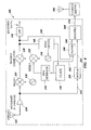
- FIG. 4 illustrates one embodiment of a DSSS communication system of the present invention, generally indicated by the numeral 180 .
- DSSS system 180 includes a first receiver 200 and a corresponding first transmitter 300 , as well as a second receiver 400 and a corresponding second transmitter 500 .
- a power level control signal is subsequently fed or relayed back to the transmitter 300 via the second transmitter and receiver pair, where it is used to adjust the output or transmit power level of the first transmitter 300 .
- the power level control signal generated by receiver 200 is configured so as to adjust the output power of the first transmitter 300 towards the minimum power level necessary for reliable communication of information between the first transmitter and receiver pair.
- transmitter 300 and feedback receiver 400 could be integrally combined so as to effectively form a first communications transceiver module.
- receiver 200 and feedback transmitter 500 could be integrally combined so as to effectively form a second communications transceiver module.
- the feedback transmitter and receiver pair need not necessarily employ a spread spectrum communication technique.
- spread spectrum transmitter 300 can include spread spectrum signal receiving capabilities
- spread spectrum receiver 200 can include spread spectrum transmitting capabilities to form a spread spectrum transceiver pair.
- both sides may include a received signal minimum necessary power level calculation circuit for producing a signal for adjusting the transmitted power from the other side. The internal details and interworkings of such an exemplary received signal minimum necessary power level calculation circuit will be discussed in more detail below.
- the basis of the power level control signal computation involves a unique property of spread spectrum communication systems. As discussed previously, signals generated using spread spectrum techniques appear as noise in the frequency domain. The wide bandwidth provided by the spreading code effectively allows the transmitted signal power to drop below the noise threshold without loss of information.
- the power level control signal computation algorithm implemented in a DSSS receiver of the present invention capitalizes on this key characteristic of spread spectrum transmissions. More particularly, it will be appreciated by those skilled in the art that true random noise exhibits a uniform instantaneous power spectral density (P n ) distribution over a given area of bandwidth.
- FIG. 6 is a block diagram that generally illustrates the base internal architecture of one embodiment of a direct sequence spread spectrum (DSSS) receiver, generally indicated by the numeral 200 .
- DSSS receiver 200 includes a receiving antenna 122 , a broadband RF amplifier 124 , and a first signal mixer 126 .
- the output signal produced by mixer 126 is then compared at a second mixer or correlator 130 to another IF signal that is generated by a third mixer 132 .
- the IF signal generated by mixer 132 is produced using the same spreading code sequence as that used by the corresponding or matching DSSS transmitter 300 .
- This spreading code sequence is generated by a PSN generator 134 and an associated clock function 136 . More particularly, the binary spreading code sequence produced by PSN generator 134 is combined with an IF carrier signal that is produced by an IF oscillator 138 .
- signal output by the correlating mixer 130 is used to drive a synchronization circuit 140 , which in turn is responsible for insuring that the IF carrier signal generated by oscillator 138 is of the exact frequency and phase necessary for demodulation or “de-spreading” of the received broadband signal.
- Synchronization circuit 140 performs this function, in part, by altering the frequency of clock source 136 such that the PSN or spreading code chip rate matches that of the incoming modulated broadband signal. Since the spreading code produced by the PSN generator is the same as that contained within the received signal, adjusting the clock in the manner described above will eventually allow the two signals to be brought into a synchronized state.
- the spreading code produced by PSN generator 134 is used to modulate the IF carrier produced by oscillator 138 at mixer 132 .
- This spreading code modulated IF carrier output of mixer 132 is subsequently provided as one input to the correlating mixer 130 .
- the output of mixer 132 is a BPSK modulated signal that is similar to the received broadband signal.
- This BPSK modulated signal produced by mixer 132 is compared to the received broadband signal in mixer 130 , which effectively acts as a correlator.
- the correlating mixer 130 might include phase demodulating and demodulated signal processing functionality.
- the output of the correlating mixer 130 is then filtered via a Low Pass Filter (LPF) 142 so as to generally recover the original sequence of binary information sent by the first transmitter 300 .
- LPF Low Pass Filter
- RSPLM module 210 is configured so as to receive as input an amplified form of a received broadband signal from amplifier 124 . As indicated in FIG. 6 , this amplified signal is provided to RSPLM module 210 via a communication pathway or connection 212 .
- FIG. 7 is a detailed schematic diagram of one embodiment of RSPLM module 210 .
- RSPLM 210 is adapted to receive, as input, the amplified broadband signal 212 and subsequently generate an output signal that is proportional to the power level of the input signal.
- FIG. 7 is a block diagram illustrating internal details of RSPLM module 210 .
- RSPLM module 210 includes a multiplier 216 and a low pass filter 218 .
- Multiplier 216 is configured so as to take as input the broadband signal received over connection 212 and effectively output a signal that is the mathematical square of this input signal.
- the squared output signal is subsequently subjected to the low pass filter 218 , with the passed signal component being output from the RSPLM module as output signal U 2 (P sum , t).
- signal U 2 (P sum , t) is proportional to the power level of the received user data signal. More particularly, the signal U 2 (P sum , t) represents a voltage proportional to the total power of the received signal, which includes the useful signal, noise of the transmission medium, including active interference and noise produced by input devices.
- RSPLM module 210 can be implemented using a variety of architectures other than that specifically shown in FIG. 7 .
- RSPLM module 210 could be implemented in hardware, software, firmware, or a combination thereof.
- RSPFM module 240 is configured so as to receive as input a phase demodulated and “de-spread” received signal after processing by the correlating mixer 130 .
- phase demodulated and “de-spread” received signal it will be appreciated that following processing by correlating mixer 130 , such a recovered signal ideally directly reflects the information or payload component of the broadband signal originally transmitted by transmitter 300 .
- This recovered information signal is provided to RSPFM module 240 via a communication pathway or connection 242 , as indicated in FIG. 6 .
- Received signal phase fluctuation measurement module 240 also receives the clock signal output from clock module 136 via connection 243 .
- FIG. 8 is a detailed schematic diagram of one embodiment of RSPFM module 240 .
- RSPFM module 240 includes a maximum signal voltage level measurement module 246 , a minimum signal voltage level measurement module 248 , a signal voltage level difference calculation module 250 , and a signal voltage level normalizer 252 .
- the minimum and maximum signal level measurement modules 248 and 246 are adapted to receive the phase demodulated and “de-spread” received signal after processing by the correlating mixer 130 via signal connection 242 and the clock signal output from the clock module 136 via connection 243 .
- maximum signal level measurement module 246 analyzes the input signal over intervals determined by the clock signal received over connection 243 which corresponds the chip sequence frequency, and subsequently produces an output signal that is representative of the absolute maximum voltage level of the same input signal (V max ) over the defined interval.
- absolute minimum signal level measurement module 248 analyzes the input signal over intervals determined by the clock signal received over connection 243 which corresponds to the chip sequence frequency, and subsequently produces an output signal that is representative of the average minimum voltage level of the input signal (V min ).
- Module 246 includes a voltage controlled switch 501 , a first capacitor 502 , a second capacitor 504 , a diode 506 , and a resistor 508 .
- the output of this circuit is a signal representative of the maximum amplitude of input signal received over connection 242 .
- switch 501 closes in response to the clock signal received over connection 243
- a filtered version of input signal received over connection 242 is applied to the input terminal of diode 506 .
- Diode 506 passes the positive portion of the filtered input signal and charges capacitor 504 to the maximum level of the input signal. Accordingly, the signal V max has a level equal to the maximum level of the input signal received over connection 242 .
- Module 248 includes a voltage controlled switch 510 , a first capacitor 512 , a second capacitor 514 , a diode 516 , and a resistor 518 .
- the output of this circuit is a signal representative of the minimum amplitude of the input signal received over connection 242 .
- switch 510 closes in response to the clock signal received over connection 243 a current is produced through diode 516 only when the voltage level of the input signal received over connection 242 is lower than the voltage level of the output node. Current flowing from ground to diode 516 through capacitor 514 charges capacitor 514 . This charge is proportional to the minimum received voltage V min .
- FIG. 9 c illustrates an example of voltage difference calculation module 250 .
- voltage difference module 250 comprises a differential amplifier configured to produce an output signal proportional to the difference between the voltages at the inverting and noninverting input terminals.
- the differential amplifier circuit includes an operational amplifier 520 with a feedback resistor 522 and input resistors 524 , 526 , and 528 .
- V 0 ( R 526 + R 522 R 524 + R 528 ) ⁇ R 528 R 526 ⁇ V max - R 522 R 526 ⁇ V min , ( 1 ) where the resistor subscripts in Equation 1 correspond to the resistor numbers in FIG. 9 C.
- module 250 produces a signal that is proportional to the difference between the maximum and minimum voltage levels of the received signal in case when all of the resistors are equal to each other.
- FIG. 9 d is a block diagram of an exemplary normalizer module according to an embodiment of the present invention.
- normalizer module 252 includes first and second operational amplifiers 530 and 532 , multiplier 534 , and inputer resistor 536 .
- the equation for the output signal of normalizer module 252 is V max - V min V max , assuming that operational amplifiers 530 and 532 are ideal. Accordingly, normalizer module 252 produces a signal that is proportional to the normalized difference between the maximum and minimum values of the demodulated spread spectrum signal over the defined interval.
- phase fluctuation measurement function performed by RSPFM module 240 can be implemented using a variety of architectures other than that specifically shown in FIG. 8 .
- RSPFM module 240 could be implemented in hardware, software, firmware, or a combination thereof.
- RSMNPLC module 260 is configured so as to receive input signals from both RSPLM module 210 and RSPFM module 240 via connections 214 and 244 , respectively.
- FIG. 10 is a block diagram of an exemplary configuration for RSMNPLC module 260 according to an embodiment of the present invention.
- RSMNPLC module 260 includes a reference voltage normalizer module 262 , which is similar in operation and structure to normalizer 252 illustrated with respect to FIG. 9 d . Accordingly, it will be appreciated that reference voltage normalizer module 262 produces an output signal based on the output signal from normalizer 252 and a reference voltage V ref output from reference voltage generator 264 . The value of V ref is selected based on the maximum allowed value of the signal to noise ratio, which depends on the noise resistance of the given modulation and coding techniques.
- Operation module 268 produces a code on bus 270 for controlling the mode of operation of feedback transmitter 500 .
- code 270 is formed includes comparators 1002 and 1004 , a sample-and-hold (SH) circuit 1006 , and a sample-and-hold control signal formation circuit (SH CSF) 1008 including an OR gate 1010 and differentiating circuits 1012 and 1014 .
- SH sample-and-hold
- SH CSF sample-and-hold control signal formation circuit
- the signal produced by the RSPFM module and input to RSMNPLC module 260 via connection 244 is the equivalent of sin 2 ( ⁇ ), which is the ratio of true noise power density to information signal power density (P n /P s ).
- ⁇ is defined as a phase fluctuation angle associated with the information signal.
- the input signal produced by RSPLM module 210 received via connection 214 is referred to as P sum , and is representative of the power level of the received user data or information signal.
- connection 244 The input signal received from connection 244 is directed to reference voltage normalizer 262 , along with a reference voltage signal, V Ref , from the reference voltage source 264 .
- Reference voltage normalizer 262 subsequently produces an output signal 266 which can be expressed as sin 2 ( ⁇ )/sin 2 ( ⁇ max ).
- the output signal on connection 266 is calculated as the ratio of the input signal sin 2 ( ⁇ ) to the source of sample power sin 2 ( ⁇ max ).
- FIG. 10 illustrates module 260 , which includes modules 262 (normalizer), 264 —the source of the reference voltage corresponding to the maximum allowed value of the noise to signal ratio, which depends on the noise resistance of the given modulation and coding type, and module 268 —the operational module which determines the mode of operation of module 500 , and module 272 (multiplexer).
- modules 262 normalizer
- 264 the source of the reference voltage corresponding to the maximum allowed value of the noise to signal ratio, which depends on the noise resistance of the given modulation and coding type
- module 268 the operational module which determines the mode of operation of module 500
- module 272 multiplexer
- connection 214 the signal input via connection 214 .
- this signal along with a reference voltage signal from reference voltage source 264 and the input signal received via connection 244 are provided as inputs to operational module 268 .
- the signal received via connection 244 comes to the first input of module 260 from module 240 and corresponds to the signal to noise ratio of the received signal.
- the first input of module 260 is connected to the input of module 262 (normalizer) and to the second input of module 268 (operational module).
- the signal received via connection 244 is normalized according to the level of the reference signal coming to the reference signal input of module 262 from module 264 . So, in module 262 a signal is formed, the voltage of which corresponds to the ratio of signal received via connection 244 to the signal coming from module 264 .
- the formula of this ratio is U 2 (t) ⁇ P min /P s ⁇ sin 2 ⁇ /sin 2 ⁇ max .
- the signal output from module 262 is input to multiplexer 272 .
- comparator 1002 The voltage of the signals received via connection 244 and output from reference voltage generator 264 are compared by comparator 1002 .
- Sample-and-hold control signal formation circuit 1008 under the influence of the voltage coming through one of the differentiating units produces the sample voltage which comes to the controlling input of switch 1016 in sample-and-hold circuit 1006 , which is closed by this voltage.
- the time of action of the sample impulse voltage is selected so that it is sufficient to charge capacitor 1018 from the charge on capacitor 1020 connected to the input of switch 1016 .
- comparator 1002 the voltage from its non-inverting output comes also to the bus 270 and determines the state of one of the digits of the code transmitted through this bus.
- sample-and-hold circuit 1006 switches on from the voltage coming from the inverting output of comparator 1002 through differentiating circuit 1004 to the second input of OR gate 1010 . At that moment the voltage from the non-inverting output of comparator 1002 comes to the bus 270 and changes the code digit to the opposite voltage.
- the voltage of the signal received via connection 214 corresponding to the voltage of the received signal P sum comes through the second input of module 260 to the remaining input of module 268 , is differentiated by RC circuit 1022 and comes to the non-inverting input of comparator 1004 where it is compared to the voltage coming from resistor 1024 , which determines the threshold level of comparator 1004 .
- the dynamic component of the signal received via connection 214 coming from the non-inverting input of comparator 1064 is greater than the voltage at the inverting input, which is selected somewhat greater than the voltage of circuit instability recalculated to the non-inverting input of comparator 1004 , at the output of comparator 1004 a voltage equal to logical value “true” is generated.
- the signal output from comparator 1004 comes through integrating circuit 1026 connected to the output of comparator 1004 and through switch 1016 to capacitor 1018 , and charges capacitor 1018 during the connected state of switch 1016 .
- the second digit of the code on bus 270 is determined by the voltage of switch 1016 .
- Differentiating circuit 1022 connected to the input of comparator 1004 is resistant to signals with the length close to or greater than the length of the package.
- the two bit binary code 270 output from RSMNPLC 260 determines whether the difference between sin 2 ( ⁇ ) and sin 2 ( ⁇ max ) is the result of noise or the end of package transmission of useful information.
- This binary code information along with the calculated ratio of instantaneous signal power to the minimum instantaneous acceptable signal power at a given signal noise power level is subsequently broadcast back to the “originating” DSSS transmitter 300 , which in turn uses this information to “decide” whether it is necessary to change the signal power during the next data transmission.
- the feedback control component signals 266 and 270 are provided as input to the signal multiplexing module 272 which is adapted to multiplex the multiple signal components into a serial bit stream 274 that is suitable for transmission back to the “originating” DSSS transmitter 300 .
- DSSS transmitter 300 includes a PSN code generator 104 , which is adapted to receive input from a high frequency clock source. Coupled to the output of PSN code generator 104 is a logic “exclusive OR” or XOR gate 106 . XOR gate 106 is also configured to take as input, a user data stream 102 . The “spread” signal output from XOR gate 106 is then directed to a BPSK modulating process 108 , where the signal is BPSK modulated with the aid of a carrier oscillator 110 .
- a variable power amplifier (VPA) 302 is adapted to receive the BPSK modulated signal as well as a power level feedback control signal 306 .
- Power level feedback control signal 306 is provided by a Feedback Signal Controller (FSC) 304 , which is adapted to receive, de-multiplex, and process the received power level feedback control signal 410 so as to insure that the power control information is in a format that is compatible with VPA 302 .
- Power level feedback control signal 306 is used to adjust the output power level of VPA 302 .
- the amplified output signal produced by VPA 302 is subsequently broadcast via a transmission antenna 114 .
- FSC process 304 it will be appreciated that in an alternate embodiment the de-multiplexing operation performed by this process could easily be performed at the receiver where the power level control signal is received. In such a case, FSC process 304 would simply receive the two bit binary code and perform any pre-processing or formatting required to meet the operational specifications of the associated VPA 302 .
- This power regulation can be performed by known methods, for example by changing voltage of the power supply at the transmitter power amplifier 302 (recommended in cases when the transmitter operates in the modes corresponding to cases 3 and 4), and also by providing power supply to all the output cascades of the transmitter 302 which use the principle of power addition (recommended for the case of corresponding transmitter design), as well as by signal level control for intermediate cascades of the transmitter 500 ( 302 ) (recommended for transmitters, the output cascades of which operate in linear mode corresponding to case 1) etc.
- FSC 304 illustrated in FIG. 11 represents a demultiplexer which forms from the power level feedback control signal received via connection 310 a signal output over connection 306 to control the output power of variable power amplifier 302 .
- the signal on connection 306 may represent a digital code, an analog signal, or a combined digital and analog signal depending on the method for controlling the output of variable power amplifier 302 .
- the selection of the control mechanism for variable power amplifier 302 may be any mechanism known by those of ordinary skill in the art and is not the subject of the present invention.
- the power level feedback control signal is provided to DSSS transmitter 300 by the associated feedback receiver 400 .
- a DSSS system 180 includes a first transceiver unit that is comprised of a DSSS transmitter component 300 and feedback receiver component 400 . Also included is a second transceiver unit that is similarly comprised of a DSSS receiver component 200 and a feedback transmitter component 500 . From a high-level functional standpoint, the real-time transmission power level control feedback loop is established in DSSS system 180 as DSSS transmitter 300 formulates and broadcasts a spread spectrum broadband signal. This broadband signal is received and generally decoded by DSSS receiver 200 .
- DSSS receiver 200 uses the received broadband signal to generate a power level control signal that is subsequently broadcast by feedback transmitter 500 and received by feedback receiver 400 .
- Feedback receiver 400 communicates the received power level control signal information to DSSS transmitter 300 which, in turn, uses this control information to adjust its transmission power level.
- the same power level control feedback loop could be implemented between feedback transmitter 500 and feedback receiver 400 , so as to generally establish a system wide or bi-directional closed-loop feedback configuration. As such, optimal transmission power levels can be maintained in real or near-real time within the DSSS communication system of the present invention.
- a binary data stream 102 representing useful or user data is input to the transmitter from an external data source, as indicated in FIG. 11 .
- This user data stream 102 is combined at XOR gate 106 with a spreading code sequence that is generated by PSN code generator 104 .
- the resulting encoded or “spread” user data signal is then modulated using a BPSK scheme by BPSK modulator 108 .
- the modulated user data signal is then amplified to a particular power level by VPA 302 .
- the modulated user data signal may be amplified to a relatively high power level, so as to ensure that the corresponding DSSS receiver 200 has the best chance of successfully receiving the signal and decoding the user data. Subsequent feedback control iterations might then act to reduce the VPA power level, so as generally seek the minimum necessary transmission power level required for successful and reliable reception of the user signal.
- the “spread”, modulated, and amplified user data signal is received by DSSS receiver 200 via the receiving antenna 122 , as indicated in FIG. 6 .
- the weak, received user data signal is amplified by RF amplifier 124 and subsequently mixed with an intermediate frequency local oscillator signal generated by oscillator 128 .
- This intermediate frequency-mixed signal is then directed to the phase demodulator/demodulated signal processor or correlator 130 .
- RSPFM Received Signal Phase Fluctuation Measurement
- This recovered binary user data stream is subsequently provided as input to the Received Signal Phase Fluctuation Measurement (RSPFM) module 240 as input signal 242 .
- RSPFM module also included as input to RSPFM module is a clock signal 243 that is produced by the same oscillator 136 which drives PSN code generator 134 .
- maximum and minimum signal amplitude detectors 246 and 248 respectively, produce signals that enable the normalizer process 252 to effectively calculate a normalization parameter ((V max ⁇ V min )/V max ) related to the binary user data stream.
- This normalization parameter is output from RSPFM module 240 as signal 244 .
- the received user data signal is tapped immediately following amplification by RF amplifier 124 and prior to mixing with the heterodyne frequency generated by oscillator 128 .
- This encoded and modulated user data signal is provided as input to the Received Signal Power Level Measurement (RSPLM) module 210 , where the signal is subsequently multiplied by itself or effectively squared by multiplier process 216 , as indicated in FIG. 7 .
- the result of this squaring process is then filtered and output from RSPLM module 210 as output signal 214 .
- this output signal is referred to as P sum , and is representative of the instantaneous power level of the received user data or information signal.
- RSPFM module 240 the minimum and maximum signal level measurement modules 248 and 246 , respectively, are each adapted to receive the phase demodulated and “de-spread” received signal via signal connection 242 , as shown in FIGS. 6 and 8 .
- the output signals produced by the maximum and minimum voltage level detectors 246 and 248 , respectively, are provided as input to the signal voltage level difference calculation process 250 .
- Difference calculation process 250 generates an output signal that is proportional to the difference in magnitudes of maximum and minimum signal voltage levels.
- the output signals from both the maximum signal level measurement module 246 and the signal voltage level difference calculation process 250 are provided as inputs to the signal voltage level normalizer process 252 , where the difference input signal is normalized with respect to the maximum voltage level input signal, thereby essentially computing the ratio of the difference input signal to the maximum voltage level signal ((V max ⁇ V min )/V max ).
- This normalized signal which is the approximate equivalent of sin 2 ( ⁇ ), is subsequently output via connection 244 .
- RSMNPLC module 260 is adapted to receive the normalized signal ad 244 , as well as the instantaneous power level of the received user data or information signal, P sum 214 . These two input signals, in conjunction with a reference voltage signal that is generated within the RSMNPLC, process are employed to produce a pair of power level control feedback signals, 266 and 270 .
- Feedback control signal component 266 is indicative of the ratio of instantaneous signal power to the minimum instantaneous acceptable signal power at a given signal noise power level, while the two bit binary control signal 270 essentially indicates whether the difference between sin 2 ( ⁇ ) and sin 2 ( ⁇ max ) is the result of noise or is instead an artifact of the end of a package transmission of useful information.
- these two power level control signal components are multiplexed into a serial bit stream 274 and subsequently broadcast back to the “originating” DSSS transmitter 300 , which in turn uses this information to “decide” whether it is necessary to change the signal power during the next data transmission. More particularly, it will be appreciated from FIG. 111 that feedback receiver 400 receives the power level control signal information that is broadcast by the associated feedback transmitter 500 . In the embodiment described herein, receiver 400 delivers the multiplexed power level control information signal 410 to the feedback signal controller 304 , where any necessary de-multiplexing and control signal re-construction operations are performed. A VPA compatible power level control signal 306 is then provided to the associated VPA 302 where power level control is asserted.
Abstract
Description
P sum =P n +P s.
The above relationship is graphically illustrated in the vector diagram presented in FIG. 5.
P n =P s*sin2(θ).
P n /P s−min=sin2(θmax).
P s−min /P s=sin2(θ)/sin2(θmax);
and it is this ratio of Ps−min to Ps that comprises the power level control feedback signal which is employed in the communication system of the present invention. Implementation of the above stated algorithm that defines this, ratio of Ps−min to Ps, and consequently the power level control feedback signal, is discussed in detail below.
where the resistor subscripts in
assuming that
-
- 1. In the case when the moment corresponding to fluctuation (sin2θ) exceeding the allowed fluctuation level (sin2θmax) coincides with the process of increasing power of the signal Psum, the signal code (11) appears on
bus 270, corresponding to the break-up of receiving due to increased noise. Under the influence of this code,feedback transmitter 500 sends a signal instructing the other side to immediately raise transmission power to the maximum level or to increase transmission power in a stepwise manner until receiving the answer from the other side, or until receiving a successfully transmitted packet. This code, when transmitted overbus 270, causes the turning on of thefeedback transmitter 500 in the maximum power mode. - Also, under the influence of this code transmitted through the
connection line 274,module 500 must switch to the signal (“service” packet) transmission mode, switching the transmitter of the other side into the mode of maximum power packet transmission, or with power being raised stepwise up to the allowed limit until reliable data receiving by the station wheremodule 260 is located becomes possible. -
Case 1 can be summarized as follows: - When received signal power is increasing due to noise, the signal code (11) is produced on
bus 270 to instruct the transmitter on the other side to increase signal power to its maximum value. This power increase to the maximum value is independent of the measured ratio Pmin to Ps, as evinced by the signal output fromnormalizer 262 viaconnection 266. Moreover, when the broadband noise affects the transmitter power level control signal and the received spread spectrum signal in a similar manner, the code (11) onbus 270 can be used to increase the power level offeedback transmitter 500. - 2. In the case when the moment corresponding to the exceeding of the fluctuation (sin2θ) over the maximum allowed fluctuation level (sin2θmax), coincides with the process of decreasing of the power of the received signal Psum code signal (10) appears on
bus 270 corresponding to the normal end of packet transmission. This code coming through thebus 274, causesmodule 500 to switch to the transmission mode of the “service” packet, corresponding to normal transmission completion, with the same power determined by the “service” packet received from the transmitting station for the control of the power of the receiving station. - This code, transmitted through the
transmission connection 274 by thefeedback transmitter 500, must affect the transmitter of the other side so that it transmits the next packet with the power corresponding to signal 266 (U2 (t)˜Pmin/Ps˜sin2θ/sin2θmax), which is determined by the ratio of the minimum allowed transmitter power to the actual power during the transmission of the previously transmitted packet. -
Case 2 can be summarized as follows: - The code (10) on
bus 270 is used to command thetransmitter 300 on the other side to reduce, leave unchanged, or increase the power based on the ratio Pmin to Ps as evinced by thesignal 266 calculated during the previous packet. This code can also be used to adjust, i.e., reduce, increase, or leave unchanged, the power offeedback transmitter 500 on the other side based on the service packet received from the other side, in the case of a symmetrical communications system. Again, such control of the feedback transmitter power is possible in the case where noise similarly influences the spread spectrum broadband signal and the transmitter control signal. This can occur when the frequency bands of both channels are the same and modulation types of both channels are similar. - 3. In the case when transmission becomes possible (sin2θ passes a minimum threshold) due to the increased power Psum, the code (01) is generated, which comes through the
bus 274,switches module 500 into the mode, in which it must, if necessary, operate as usual based on the information received from the other side, if the situation doesn't change until the end of the received packet, as in case of code (10). -
Case 3 can be summarized as follows: - The code (01) is generated when the received power level exceeds the minimum threshold. However, the code (01) can only be used for switching
feedback transmitter 500 into a mode in which it would be operating after the normal completion of a packet (case 2), if before the end of the packet there is no termination of receiving, which would lead tocase 1. The code (01) is not used for controlling the power oftransmitter 300 on the other side since the code (01) is generated at the beginning of a packet and is used to the end of the packet if there is no feedback. - 4. In the case when the receiving under the conditions of reduced noise level, of which the reduction of Psum is sign of, code (00) is being generated.
- Case 4 can be summarized as follows:
- The code (00) is generated when the noise level is reduced, and the receiving started after reduction of the noise level. The code (00) can be preceded only by the code (11), which may signify the loss of the connection during transmission of preceding packets. Therefore, the code (00) prevents the transmitter on the other side from reducing power.
- The following is a summary of the codes that can appear on
bus 270.- Code (11)—increase of the transmitter power to the maximum (one time or step wise) despite the ratio of Pmin to Ps
- Code (10)—requires adjustment of the power level according to the ratio of Pmin to Ps
- Code (00)—prevents the transmitter from reducing power despite the ratio of Pmin to Ps
- Code (01)—not used in power control.
- 1. In the case when the moment corresponding to fluctuation (sin2θ) exceeding the allowed fluctuation level (sin2θmax) coincides with the process of increasing power of the signal Psum, the signal code (11) appears on
Claims (26)
Priority Applications (1)
| Application Number | Priority Date | Filing Date | Title |
|---|---|---|---|
| US09/636,177 US6853675B1 (en) | 2000-08-10 | 2000-08-10 | Methods and systems for optimizing signal transmission power levels in a spread spectrum communication system |
Applications Claiming Priority (1)
| Application Number | Priority Date | Filing Date | Title |
|---|---|---|---|
| US09/636,177 US6853675B1 (en) | 2000-08-10 | 2000-08-10 | Methods and systems for optimizing signal transmission power levels in a spread spectrum communication system |
Publications (1)
| Publication Number | Publication Date |
|---|---|
| US6853675B1 true US6853675B1 (en) | 2005-02-08 |
Family
ID=34104622
Family Applications (1)
| Application Number | Title | Priority Date | Filing Date |
|---|---|---|---|
| US09/636,177 Expired - Fee Related US6853675B1 (en) | 2000-08-10 | 2000-08-10 | Methods and systems for optimizing signal transmission power levels in a spread spectrum communication system |
Country Status (1)
| Country | Link |
|---|---|
| US (1) | US6853675B1 (en) |
Cited By (23)
| Publication number | Priority date | Publication date | Assignee | Title |
|---|---|---|---|---|
| US20020051434A1 (en) * | 1997-10-23 | 2002-05-02 | Ozluturk Fatih M. | Method for using rapid acquisition spreading codes for spread-spectrum communications |
| US20020057659A1 (en) * | 1995-06-30 | 2002-05-16 | Ozluturk Fatih M. | Apparatus for adaptive forward power control for spread-spectrum communications |
| US20020118653A1 (en) * | 1995-06-30 | 2002-08-29 | Interdigital Technology Corporation | Automatic power control system for a code division multiple access (CDMA) communications system |
| US20040066200A1 (en) * | 2002-10-08 | 2004-04-08 | Mitsubishi Denki Kabushiki Kaisha | Vehicular alternator failure determination apparatus |
| US20040114670A1 (en) * | 2002-12-13 | 2004-06-17 | International Business Machines Corporation | System and method for transmitting data and additional information simultaneously within a wire based communication system |
| US20040198371A1 (en) * | 2003-04-01 | 2004-10-07 | Srinivasan Balasubramanian | Scalable quality broadcast service in a mobile wireless communication network |
| US20040252668A1 (en) * | 1995-06-30 | 2004-12-16 | Interdigital Technology Corporation | Code division multiple access (CDMA) communication system |
| US20050030935A1 (en) * | 2001-11-26 | 2005-02-10 | Claus Seisenberger | Method and device for the synchronization of radio stations and a time-synchronous radio bus system |
| US20050094604A1 (en) * | 1995-06-30 | 2005-05-05 | Interdigital Technology Corporation | Initial power control for spread-spectrum communications |
| US20050265062A1 (en) * | 2004-05-26 | 2005-12-01 | Robert Walker | Chip to chip interface |
| US20050265430A1 (en) * | 1995-06-30 | 2005-12-01 | Interdigital Technology Corporation | System for using rapid acquisition spreading codes for spread-spectrum communications |
| US20060223448A1 (en) * | 2005-04-05 | 2006-10-05 | Cisco Technology, Inc. | Method and system for coordinating radio resources in unlicensed frequency bands |
| US20060270433A1 (en) * | 2005-05-31 | 2006-11-30 | Kelton James R | Adjusting transmit power of a wireless communication device |
| US20070147251A1 (en) * | 2005-09-23 | 2007-06-28 | Peter Monsen | Technique for adaptive data rate communication over fading dispersive channels |
| US20070184782A1 (en) * | 2006-02-03 | 2007-08-09 | Sahota Gurkanwal S | Baseband transmitter self-jamming and intermodulation cancellation device |
| US7839916B1 (en) * | 2003-10-08 | 2010-11-23 | L-3 Communications Corporation | Systems and methods for communication in a global positioning system (GPS) device |
| WO2011009027A1 (en) * | 2009-07-17 | 2011-01-20 | Sensis Corporation | System and method for data communications on dme transponder links |
| WO2013003633A1 (en) * | 2011-06-29 | 2013-01-03 | Comtech Ef Data Corp. | Embedded meta-carrier with code progression message reassembly |
| US20140050253A1 (en) * | 2012-08-16 | 2014-02-20 | Andrew Wireless Systems Gmbh | Reducing Distortion in Repeaters for OFDM Signals |
| US20150280957A1 (en) * | 2014-03-25 | 2015-10-01 | Electronics And Telecommunications Research Institute | Method and apparatus for transmitting and receiving |
| US20150303987A1 (en) * | 2013-01-08 | 2015-10-22 | Murata Manufacturing Co., Ltd. | Spread spectrum communication device |
| US9904403B2 (en) * | 2015-06-30 | 2018-02-27 | Synaptics Incorporated | RF emission spectrum randomization and targeted nulling for an electronic device |
| WO2019034077A1 (en) * | 2017-08-15 | 2019-02-21 | 中兴通讯股份有限公司 | Power consumption control method and device and computer readable storage medium |
Citations (7)
| Publication number | Priority date | Publication date | Assignee | Title |
|---|---|---|---|---|
| US5267262A (en) | 1989-11-07 | 1993-11-30 | Qualcomm Incorporated | Transmitter power control system |
| US5383219A (en) | 1993-11-22 | 1995-01-17 | Qualcomm Incorporated | Fast forward link power control in a code division multiple access system |
| US5487180A (en) | 1993-09-20 | 1996-01-23 | Fujitsu Limited | Method of determining initial transmission power |
| US6035209A (en) | 1995-03-31 | 2000-03-07 | Qualcomm Incorporated | Method and apparatus for performing fast power control in a mobile communication system |
| US6088573A (en) * | 1997-05-28 | 2000-07-11 | Nec Corporation | Transmission power control method and apparatus for mobile radio satellite communication system |
| US6278701B1 (en) * | 1998-07-10 | 2001-08-21 | Verizon Laboratories Inc. | Capacity enhancement for multi-code CDMA with integrated services through quality of services and admission control |
| US6298220B1 (en) * | 1998-01-15 | 2001-10-02 | Hughes Electronics Corporation | Power control system for communications channels |
-
2000
- 2000-08-10 US US09/636,177 patent/US6853675B1/en not_active Expired - Fee Related
Patent Citations (7)
| Publication number | Priority date | Publication date | Assignee | Title |
|---|---|---|---|---|
| US5267262A (en) | 1989-11-07 | 1993-11-30 | Qualcomm Incorporated | Transmitter power control system |
| US5487180A (en) | 1993-09-20 | 1996-01-23 | Fujitsu Limited | Method of determining initial transmission power |
| US5383219A (en) | 1993-11-22 | 1995-01-17 | Qualcomm Incorporated | Fast forward link power control in a code division multiple access system |
| US6035209A (en) | 1995-03-31 | 2000-03-07 | Qualcomm Incorporated | Method and apparatus for performing fast power control in a mobile communication system |
| US6088573A (en) * | 1997-05-28 | 2000-07-11 | Nec Corporation | Transmission power control method and apparatus for mobile radio satellite communication system |
| US6298220B1 (en) * | 1998-01-15 | 2001-10-02 | Hughes Electronics Corporation | Power control system for communications channels |
| US6278701B1 (en) * | 1998-07-10 | 2001-08-21 | Verizon Laboratories Inc. | Capacity enhancement for multi-code CDMA with integrated services through quality of services and admission control |
Cited By (49)
| Publication number | Priority date | Publication date | Assignee | Title |
|---|---|---|---|---|
| US20050094604A1 (en) * | 1995-06-30 | 2005-05-05 | Interdigital Technology Corporation | Initial power control for spread-spectrum communications |
| US20040071198A1 (en) * | 1995-06-30 | 2004-04-15 | Interdigital Technology Corporation | Code detection |
| US20090103508A1 (en) * | 1995-06-30 | 2009-04-23 | Interdigital Technology Corporation | Automatic power control system for a code division multiple access (cdma) communications system |
| US7903613B2 (en) | 1995-06-30 | 2011-03-08 | Interdigital Technology Corporation | Code division multiple access (CDMA) communication system |
| US20050243897A1 (en) * | 1995-06-30 | 2005-11-03 | Interdigital Technology Corporation | Rapid acquisition spreading codes for spread-spectrum communications |
| US20100157950A1 (en) * | 1995-06-30 | 2010-06-24 | Interdigital Technology Corporation | System for using rapid acquisition spreading codes for spread-spectrum communications |
| US20040165654A1 (en) * | 1995-06-30 | 2004-08-26 | Interdigital Technology Corporation | Efficient multipath centroid tracking circuit for a code division multiple access (CDMA) system |
| US7706332B2 (en) | 1995-06-30 | 2010-04-27 | Interdigital Technology Corporation | Method and subscriber unit for performing power control |
| US20040252668A1 (en) * | 1995-06-30 | 2004-12-16 | Interdigital Technology Corporation | Code division multiple access (CDMA) communication system |
| US20100002752A1 (en) * | 1995-06-30 | 2010-01-07 | Interdigital Technology Corporation | Efficient multipath centroid tracking circuit for a code division multiple access (cdma) system |
| US20020118653A1 (en) * | 1995-06-30 | 2002-08-29 | Interdigital Technology Corporation | Automatic power control system for a code division multiple access (CDMA) communications system |
| US20020057659A1 (en) * | 1995-06-30 | 2002-05-16 | Ozluturk Fatih M. | Apparatus for adaptive forward power control for spread-spectrum communications |
| US7756190B2 (en) | 1995-06-30 | 2010-07-13 | Interdigital Technology Corporation | Transferring voice and non-voice data |
| US20050265430A1 (en) * | 1995-06-30 | 2005-12-01 | Interdigital Technology Corporation | System for using rapid acquisition spreading codes for spread-spectrum communications |
| US20100272155A1 (en) * | 1995-06-30 | 2010-10-28 | Interdigital Technology Corporation | Code detection |
| US9564963B2 (en) | 1995-06-30 | 2017-02-07 | Interdigital Technology Corporation | Automatic power control system for a code division multiple access (CDMA) communications system |
| US8737363B2 (en) | 1995-06-30 | 2014-05-27 | Interdigital Technology Corporation | Code division multiple access (CDMA) communication system |
| US7929498B2 (en) | 1995-06-30 | 2011-04-19 | Interdigital Technology Corporation | Adaptive forward power control and adaptive reverse power control for spread-spectrum communications |
| US20020051434A1 (en) * | 1997-10-23 | 2002-05-02 | Ozluturk Fatih M. | Method for using rapid acquisition spreading codes for spread-spectrum communications |
| US7940743B2 (en) * | 2001-11-26 | 2011-05-10 | Symeo Gmbh | Method and device for the synchronization of radio stations and a time-synchronous radio bus system |
| US20050030935A1 (en) * | 2001-11-26 | 2005-02-10 | Claus Seisenberger | Method and device for the synchronization of radio stations and a time-synchronous radio bus system |
| US6977487B2 (en) * | 2002-10-08 | 2005-12-20 | Mitsubishi Denki Kabushiki Kaisha | Vehicular alternator failure determination apparatus using commutating device voltage |
| US20040066200A1 (en) * | 2002-10-08 | 2004-04-08 | Mitsubishi Denki Kabushiki Kaisha | Vehicular alternator failure determination apparatus |
| US7346094B2 (en) * | 2002-12-13 | 2008-03-18 | International Business Machines Corporation | System and method for transmitting data and additional information simultaneously within a wire based communication system |
| US20040114670A1 (en) * | 2002-12-13 | 2004-06-17 | International Business Machines Corporation | System and method for transmitting data and additional information simultaneously within a wire based communication system |
| US7400889B2 (en) * | 2003-04-01 | 2008-07-15 | Telefonaktiebolaget Lm Ericsson (Publ) | Scalable quality broadcast service in a mobile wireless communication network |
| US20040198371A1 (en) * | 2003-04-01 | 2004-10-07 | Srinivasan Balasubramanian | Scalable quality broadcast service in a mobile wireless communication network |
| US7839916B1 (en) * | 2003-10-08 | 2010-11-23 | L-3 Communications Corporation | Systems and methods for communication in a global positioning system (GPS) device |
| US20050265062A1 (en) * | 2004-05-26 | 2005-12-01 | Robert Walker | Chip to chip interface |
| US20060223448A1 (en) * | 2005-04-05 | 2006-10-05 | Cisco Technology, Inc. | Method and system for coordinating radio resources in unlicensed frequency bands |
| US7526255B2 (en) * | 2005-04-05 | 2009-04-28 | Cisco Technology, Inc. | Method and system for coordinating radio resources in unlicensed frequency bands |
| US20060270433A1 (en) * | 2005-05-31 | 2006-11-30 | Kelton James R | Adjusting transmit power of a wireless communication device |
| US7751372B2 (en) | 2005-09-23 | 2010-07-06 | Peter Monsen | Technique for adaptive data rate communication over fading dispersive channels |
| US20070147251A1 (en) * | 2005-09-23 | 2007-06-28 | Peter Monsen | Technique for adaptive data rate communication over fading dispersive channels |
| US8170487B2 (en) * | 2006-02-03 | 2012-05-01 | Qualcomm, Incorporated | Baseband transmitter self-jamming and intermodulation cancellation device |
| US20070184782A1 (en) * | 2006-02-03 | 2007-08-09 | Sahota Gurkanwal S | Baseband transmitter self-jamming and intermodulation cancellation device |
| WO2011009027A1 (en) * | 2009-07-17 | 2011-01-20 | Sensis Corporation | System and method for data communications on dme transponder links |
| US8699545B2 (en) | 2010-04-08 | 2014-04-15 | Comtech Ef Data Corp. | Embedded meta-carrier with code progression message reassembly |
| US8913647B2 (en) | 2010-04-08 | 2014-12-16 | Comtech Ef Data Corp. | Embedded meta-carrier with code progression message reassembly |
| WO2013003633A1 (en) * | 2011-06-29 | 2013-01-03 | Comtech Ef Data Corp. | Embedded meta-carrier with code progression message reassembly |
| US20140050253A1 (en) * | 2012-08-16 | 2014-02-20 | Andrew Wireless Systems Gmbh | Reducing Distortion in Repeaters for OFDM Signals |
| US8837559B2 (en) * | 2012-08-16 | 2014-09-16 | Andrew Wireless Systems Gmbh | Reducing distortion in repeaters for OFDM signals |
| US20150303987A1 (en) * | 2013-01-08 | 2015-10-22 | Murata Manufacturing Co., Ltd. | Spread spectrum communication device |
| US9859948B2 (en) * | 2013-01-08 | 2018-01-02 | Murata Manufacturing Co., Ltd. | Spread spectrum communication device |
| US20150280957A1 (en) * | 2014-03-25 | 2015-10-01 | Electronics And Telecommunications Research Institute | Method and apparatus for transmitting and receiving |
| US9413582B2 (en) * | 2014-03-25 | 2016-08-09 | Electronics And Telecommunications Research Instit | Method and apparatus for transmitting and receiving |
| US9904403B2 (en) * | 2015-06-30 | 2018-02-27 | Synaptics Incorporated | RF emission spectrum randomization and targeted nulling for an electronic device |
| WO2019034077A1 (en) * | 2017-08-15 | 2019-02-21 | 中兴通讯股份有限公司 | Power consumption control method and device and computer readable storage medium |
| CN109413719A (en) * | 2017-08-15 | 2019-03-01 | 中兴通讯股份有限公司 | A kind of power consumption control method, equipment and computer readable storage medium |
Similar Documents
| Publication | Publication Date | Title |
|---|---|---|
| US6853675B1 (en) | Methods and systems for optimizing signal transmission power levels in a spread spectrum communication system | |
| US7280468B2 (en) | Apparatus for constant amplitude coded bi-orthogonal demodulation | |
| US5832022A (en) | Method and apparatus for controlling the modulation index of continuous phase modulated (CPM) signals | |
| US7020114B2 (en) | Spread spectrum communication system and method using a reference signal and a plurality of message signals | |
| US7656931B2 (en) | Hybrid spread spectrum radio system | |
| JP3390771B2 (en) | Direct sequence band spreading code chip modulator | |
| US7006583B2 (en) | Method and apparatus for receiving differential ultra wideband signals | |
| CA2679170C (en) | Synchronous spread-spectrum communications system and method | |
| JP4112632B2 (en) | Multi-rate direct sequence architecture using fixed division ratio and variable spreading code length | |
| EP0050478A2 (en) | Satellite communications system and apparatus | |
| EP0944182A2 (en) | Method and apparatus for adjusting transmission power of a CDMA terminal | |
| US4612652A (en) | Frequency hopping data communication system | |
| US4597087A (en) | Frequency hopping data communication system | |
| JPH06350562A (en) | Spread spectrum communication system | |
| US7894504B2 (en) | Coherent and non-coherent hybrid direct sequence/frequency hopping spread spectrum systems with high power and bandwidth efficiency and methods thereof | |
| EP0817396A2 (en) | Spread spectrum communications system with transmitted reference | |
| US7088766B2 (en) | Dynamic measurement of communication channel characteristics using direct sequence spread spectrum (DSSS) systems, methods and program products | |
| US7236509B2 (en) | Method of communicating information between a transmitter and a receiver using ultrawideband signals | |
| Olama et al. | Design, implementation, and evaluation of a hybrid DS/FFH spread-spectrum radio transceiver | |
| US7573933B2 (en) | Adaptive delay adjustment for transmitted reference impulse radio systems | |
| US20040141546A1 (en) | Method and apparatus for ultra wideband communications system employing a spread spectrum technique transmitting a baseband signal over a wide frequency band | |
| JPH01188130A (en) | Spread spectrum communication equipment | |
| US6094415A (en) | Vector division multiple access communication system | |
| KR960000144B1 (en) | Ds spread spectrum | |
| Wong et al. | Single tone interference rejection of code-phase multiplexed direct-sequence spread-spectrum signaling |
Legal Events
| Date | Code | Title | Description |
|---|---|---|---|
| AS | Assignment |
Owner name: UMBRELLA TECHNOLOGIES, INC., NORTH CAROLINA Free format text: ASSIGNMENT OF ASSIGNORS INTEREST;ASSIGNOR:OLEYNIK, VLADISLAV;REEL/FRAME:011011/0413 Effective date: 20000809 |
|
| AS | Assignment |
Owner name: UMBRELLA CAPITAL, LLC, FLORIDA Free format text: ASSIGNMENT OF ASSIGNORS INTEREST;ASSIGNOR:UMBRELLA TECHNOLOGIES, INC.;REEL/FRAME:011462/0443 Effective date: 20010104 |
|
| REMI | Maintenance fee reminder mailed | ||
| LAPS | Lapse for failure to pay maintenance fees | ||
| STCH | Information on status: patent discontinuation |
Free format text: PATENT EXPIRED DUE TO NONPAYMENT OF MAINTENANCE FEES UNDER 37 CFR 1.362 |
|
| FP | Lapsed due to failure to pay maintenance fee |
Effective date: 20090208 |