US7333528B1 - Multiuser DSSS-OFDM multiband for ultra wideband communications - Google Patents
Multiuser DSSS-OFDM multiband for ultra wideband communications Download PDFInfo
- Publication number
- US7333528B1 US7333528B1 US10/643,302 US64330203A US7333528B1 US 7333528 B1 US7333528 B1 US 7333528B1 US 64330203 A US64330203 A US 64330203A US 7333528 B1 US7333528 B1 US 7333528B1
- Authority
- US
- United States
- Prior art keywords
- multiband
- uwb
- multiuser
- communication system
- dsss
- Prior art date
- Legal status (The legal status is an assumption and is not a legal conclusion. Google has not performed a legal analysis and makes no representation as to the accuracy of the status listed.)
- Active, expires
Links
Images


Classifications
-
- H—ELECTRICITY
- H04—ELECTRIC COMMUNICATION TECHNIQUE
- H04L—TRANSMISSION OF DIGITAL INFORMATION, e.g. TELEGRAPHIC COMMUNICATION
- H04L5/00—Arrangements affording multiple use of the transmission path
- H04L5/02—Channels characterised by the type of signal
- H04L5/023—Multiplexing of multicarrier modulation signals
- H04L5/026—Multiplexing of multicarrier modulation signals using code division
-
- H—ELECTRICITY
- H04—ELECTRIC COMMUNICATION TECHNIQUE
- H04B—TRANSMISSION
- H04B1/00—Details of transmission systems, not covered by a single one of groups H04B3/00 - H04B13/00; Details of transmission systems not characterised by the medium used for transmission
- H04B1/69—Spread spectrum techniques
- H04B1/7163—Spread spectrum techniques using impulse radio
-
- H—ELECTRICITY
- H04—ELECTRIC COMMUNICATION TECHNIQUE
- H04L—TRANSMISSION OF DIGITAL INFORMATION, e.g. TELEGRAPHIC COMMUNICATION
- H04L27/00—Modulated-carrier systems
- H04L27/18—Phase-modulated carrier systems, i.e. using phase-shift keying
- H04L27/20—Modulator circuits; Transmitter circuits
- H04L27/2032—Modulator circuits; Transmitter circuits for discrete phase modulation, e.g. in which the phase of the carrier is modulated in a nominally instantaneous manner
- H04L27/2053—Modulator circuits; Transmitter circuits for discrete phase modulation, e.g. in which the phase of the carrier is modulated in a nominally instantaneous manner using more than one carrier, e.g. carriers with different phases
- H04L27/2057—Modulator circuits; Transmitter circuits for discrete phase modulation, e.g. in which the phase of the carrier is modulated in a nominally instantaneous manner using more than one carrier, e.g. carriers with different phases with a separate carrier for each phase state
Definitions
- This invention is generally relative to a multiuser direct sequence spread spectrum (DSSS) Orthogonal Frequency Division Multiplexing (OFDM) multiband based Ultra Wideband (UWB) Communications for short-distance wireless broadband communications.
- DSSS direct sequence spread spectrum
- OFDM Orthogonal Frequency Division Multiplexing
- UWB Ultra Wideband
- FCC is adapting unwanted emission limits for UWB communication devices that are significantly more stringent than those imposed on other Part 15 devices.
- FCC allows a wide variety of the UWB communication devices, such as high-speed home and business networking devices, subject to certain frequency and power limitations.
- An emission limitation is ⁇ 10 dBm for indoor UWB operations.
- the UWB communication devices must operate in the frequency band from 3.1 GHz to 10.6 GHz.
- the UWB communication devices should satisfy the Part 15.209 emission mask limitations for the frequency band below 960 MHz and above 960 MHz.
- Table 1 lists FCC restrictions of the emission masks (dBm) along with the frequency bands (GHz) as follows:
- FCC defines an UWB communication device where a fractional bandwidth is greater than 0.25 given by
- FB 2 ⁇ ( f H - f L f H + f L ) , ( 1 ) where f H is the upper frequency of ⁇ 10 dBm emission point, and f L is the lower frequency of ⁇ 10 dBm emission point.
- the center frequency F c of an UWB transmission system is obtained by using average of the upper and lower ⁇ 10 dBm points as follows:
- the UWB communication devices must be designed in such a way that the indoor UWB operations can only occur in the indoor environments according to indoor UWB emission masks given in Table 1.
- the UWB communication devices can be used for wireless broadband communications, particularly for a short-range high-speed data transmission that can be considered as broadband access to networks.
- an analog-to-digital (A/D) converter and a digital-to-analog (D/A) converter must operate at a very high sampling rate F s so that an UWB communication receiver can be implemented in a digital domain.
- F s sampling rate
- A/D and D/A converters for UWB transmitter and receiver.
- developing such very high-speed A/D and D/A converters may not be possible with a reasonable cost. Thereby, it is a difficult problem to apply the A/D and the D/A converters directly for an UWB communication transceiver based on a single frequency band solution.
- a single frequency band-based UWB communication transceiver does not have a flexibility and scalability for transmitting and receiving a user data.
- the single frequency band-based UWB communication transceiver may have an interference with a wireless local area network (WLAN) 802.11a transceiver without using a special filter system or other approaches since the WLAN 802.11a transceiver operates at a lower U-NII frequency range from 5.15 GHz to 5.35 GHz and at an upper U-NII upper frequency range from 5.725 GHz to 5.825 GHz.
- WLAN wireless local area network
- An OFDM is an orthogonal multicarrier modulation technique that has been extensively used in a digital audio and video broadcasting, and the WLAN 802.11a.
- the OFDM has its capability of multifold increasing symbol duration. With increasing the number of subcarriers, the frequency selectivity of a channel may be reduced so that each subcarrier experiences flat fading. Thus, an OFDM approach has been shown in a particular useful for wireless broadband communications over fading channels.
- a DSSS approach is to use a pseudorandom (PN) sequence to spread a user signal.
- the PN sequence is a stream of binary ones and zeros referred to as chips rather than bits.
- the DSSS approach can be used to separate signals coming from multiusers. Multiple access interference (MAI) among multiusers can be avoided if a set of PN sequences is designed in such a way that a low crosscorrelation among the PN sequences is obtained.
- MAI multiple access interference
- the multiuser DSSS-OFDM multiband for UWB communications is disclosed herein according to some embodiments of the present invention.
- the present invention uses eleven frequency bands as a multiband, each of the frequency bands having 650 MHz bandwidths along with OFDM modulation for a multiuser UWB communication transceiver.
- a multiband OFDM solution allows using a low speed of the A/D and D/A converters.
- a unique of the PN sequences is assigned to each user so that the multiusers can share the same each of the frequency bands to transmit and receive data based on OFDM multiband of UWB technologies.
- the OFDM is an orthogonal multicarrier modulation
- subcarriers within each of the frequency bands may be flexibility turned on or off.
- the present invention of the multiuser DSSS-OFDM multiband for UWB communications has a scalability to transmit and receive from a data rate of 503.732 Mbps by using only one of the frequency bands to the data rate of 5.541 Gbps by using all of the eleven frequency bands (or a multiband).
- a multiuser DSSS-OFDM multiband of UWB communication transmitter may comprise a multiuser encoding and spreading unit, a multiband splitter, an inverse fast Fourier transform (IFFT) unit, a filtering unit, and a multiband multicarrier modulation.
- IFFT inverse fast Fourier transform
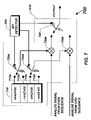
- FIG. 1 is a block diagram of a multiuser DSSS-OFDM multiband of UWB communication system with different user UWB mobile stations and a single UWB base station according to some embodiments.
- FIG. 2 is a block diagram of a multiuser DSSS-OFDM multiband for an UWB base station communication transmitter according to some embodiments.
- FIG. 3 is a detailed block diagram of a multiband splitter according to some embodiments.
- FIG. 4 is a detailed block of a 1024-point IFFT employing 1000 subcarriers and 24 NULLs according to some embodiments.
- FIG. 5 is a detailed block diagram of a filtering section according to some embodiments.
- FIG. 6 is a detailed block diagram of a multiband multicarrier modulation according to some embodiments.
- FIG. 7 is a detailed block diagram of a multiband quadrature phase shift keying (QPSK) modulation according to some embodiments.
- QPSK quadrature phase shift keying
- FIG. 8 is a detailed QPSK constellation with a mapping relationship of bits and phases.
- FIG. 9 is a frequency spectrum output of the multiuser DSSS-OFDM multiband of the UWB base station communication transmitter for the indoor UWB operations according to one embodiment.
- FIG. 10 is a block diagram of a multiuser DSSS-OFDM multiband of an UWB mobile communication receiver for a single user according to some embodiments.
- FIG. 11 is a detailed block diagram of a combination subsection including an analog bandpass filter, multiband QPSK down converters and demodulations, A/D converters, and digital receiver filters according to some embodiments.
- FIG. 12 is a detailed block diagram of a multiband QPSK demodulation and down converter according to some embodiments.
- FIG. 13 is a detailed block diagram of a combination subsection including a fast Fourier transform (FFT) and frequency-domain equalizers (FEQ) according to some embodiments.
- FFT fast Fourier transform
- FEQ frequency-domain equalizers
- FIG. 14 is a detailed block diagram of a multiband combination according to some embodiments.
- FIG. 15 is a detailed block diagram of a despreading, deinterleaver, and decoding unit for a single user of the UWB mobile communication receiver according to some embodiments.
- Some embodiments described herein are directed to the multiuser DSSS-OFDM multiband of an UWB communication system for the indoor UWB operations.
- the multiuser DSSS-OFDM multiband of UWB communication system may be implemented in hardware, such as in an Application Specific Integrated Circuits (ASIC), digital signal processor, field programmable gate array (FPGA), software, or a combination of hardware and software.
- ASIC Application Specific Integrated Circuits
- FPGA field programmable gate array
- FIG. 1 A multiuser DSSS-OFDM multiband of UWB communication system 100 for the indoor UWB operations is illustrated in FIG. 1 in accordance with one embodiment of the present invention.
- UWB mobile stations from 110 a to 110 p can communicate with an UWB base station 140 to transmit and receive information data through the frequency bands in an indoor environment simultaneously.
- An UWB mobile station 110 a transmits and receives the data through its antenna 120 a into air, and communicates with the UWB base station 140 through an antenna 130 .
- other UWB mobile stations from 110 b to 110 p also transmits and receives the data through their antennas from 120 b to 120 p , respectively, and communicate with the UWB base station 140 through the antenna 130 as well.
- the UWB base station 140 is coupled to an UWB network interface section 142 that is connected with an UWB network 144 .
- Each of the UWB mobile stations from 110 a to 110 p uses a unique PN sequence to spread and despread a user source signal. Knowing all of the PN sequences of the UWB mobile stations from 110 a to 110 p , the UWB base station 140 can transmit and receive all of the data from all of the UWB mobile stations from 110 a to 110 p based on an OFDM multiband solution by spreading and despreading of user PN sequences, respectively.
- the multiuser DSSS-OFDM multiband of the UWB communication system uses a QPSK modulation and multicarrier within each of the frequency bands to transmit and receive a data rate of 503.732 Mbps on one single frequency band up to the data rate of 5.541 Gbps on all of the eleven frequency bands. As a result, the multiuser DSSS-OFDM multiband of the UWB communication system 100 can transmit and receive a maximum data rate at 5.541 Gbps by using all of the eleven frequency bands simultaneously.
- FIG. 2 is a block diagram of the multiuser DSSS-OFDM multiband of UWB base station transmitter architecture 200 for the indoor UWB operations according to some embodiments.
- the user-1 bitstream 210 a is coupled to a 1 ⁇ 2-rate convolution encoder 212 a , which is connected to an interleaver 214 a .
- Using the unique PN sequence of a user-1 key 218 a spreads the output sequence of the interleaver 214 a .
- the users bitstream 210 p is coupled to a 1 ⁇ 2-rate convolution encoder 212 p that is connected to an interleaver 214 p .
- a 1 ⁇ 2-rate convolution encoder 212 p that is connected to an interleaver 214 p .
- the unique PN sequence of a user-p key 218 p spreads the output sequence of the interleaver 214 p .
- all of the PN sequences are orthogonal each other. This means that a cross-correlation between one PN sequence and other PN sequences is almost zero, while a self-correlation of a user PN sequence is almost equal to one.
- the p output sequences from the interleaver 214 a to the interleaver 214 p in a parallel operation are added together to form a serial sequence output by using a sum over block duration 220 .
- the serial output of the sum over block duration 220 is converted into eleven parallel sequences by using a multiband splitter 230 (see the detail illustration of the multiband splitter 230 in FIG. 3 ).
- the first of the output sequence from the multiband splitter is converted into a 512-parallel sequence by suing an serial-to-parallel (S/P) 240 a .
- the 512-parallel sequence is formed to 512-parallel complex sequence with a symmetric conjugate.
- the 512-parallel complex sequence is passed through an IFFT 242 a to produce a 1024-parallel real sequence.
- the IFFT 242 a is coupled to a guard 244 a to insert 256 samples as a guard interval for the output sequence of the IFFT 242 a .
- the output of the guard 244 a is a 1280-parallel real sequence.
- the 1280-parallel real sequences are passed through a filtering section 246 a to produce even and odd modulated signal sequences. Carriers multiply the even and odd modulated signal sequences of the filtering section 246 a by using a multiband multicarrier modulation 250 .
- the eleventh of the output sequence from the multiband splitter 230 is converted into a 512-parallel sequence by suing an S/P 240 k .
- the 512-parallel sequence is formed to 512-parallel complex sequence with the symmetric conjugate.
- the 512-parallel complex sequence is passed through an IFFT 242 k to produce a 1024-parallel real sequence.
- the IFFT 242 k is coupled to a guard 244 k to insert 256 samples as a guard interval for the output sequence of the IFFT 242 k .
- the output of the guard 244 k is a 1280-parallel real sequence.
- the guard interval is used to avoid an intersymbol interference (ISI) between IFFT frames.
- ISI intersymbol interference
- the 1280-parallel real sequences are passed through a filtering section 246 k to produce even and odd modulated signal sequences.
- Carriers multiply the even and odd modulated signal sequences of the filtering section 246 k by using a multiband multicarrier modulation 250 .
- the eleven paralleled output signal sequences of the multiband multicarrier modulation 250 are added together and passed through a power amplifier (PA) 260 into air.
- PA power amplifier
- FIG. 3 is a detailed block diagram 300 of a multiband splitter ( 230 ) architecture according to some embodiments.
- the multiband splitter ( 230 ) architecture includes ten sample delay units from 310 a to 310 k , eleven down sample units from 320 a to 320 k , eleven random access memory (RAM) units from 330 a to 330 k , and a modular counter 340 .
- An input sequence of a length of N data is divided into eleven parallel sequences with a length of N/11 data by using the sample delays from 310 a to 310 j and the down samples of 320 a to 320 k .
- the eleven output sequences of the down sample units from 320 a to 320 k are stored into RAM memories of 330 a to 330 k .
- a row size of each of the RAM units from 330 a to 330 k is 512 and the number of bits in each row can be programmed.
- a modular counter is used to control an address of the RAM units from 330 a to 330 k for storing input sequence and sending out output sequence.
- FIG. 4 is a detailed block diagram 400 of a 1024-point IFFT 410 ( 242 ) according to some embodiments.
- the rest of the input # 0 (DC) and # 501 to # 523 are set to zero.
- the coefficients from 1 to 500 are mapped to the same numbered IFFT inputs from # 1 to # 500 , while the coefficients from 500 to 1 are also copied into IFFT inputs from # 524 to # 1023 to form a complex conjugate.
- pilot signals that are assigned into the subcarriers of # 100 , # 200 , # 300 , # 400 , and # 624 , # 724 , # 824 , and # 924 .
- pilots are binary phase-shift keying (BPSK) modulated by a pseudo binary sequence to prevent a generation of spectral lines.
- BPSK binary phase-shift keying
- other 992 subcarriers of each OFDM are dedicated to assign for transmitting data information.
- an output of the 1024-point IFFT is cyclically extended to a desired length in each of the multiband.
- Table 2 lists data rate-dependent parameters of the 1024-point IFFT operation for each of the frequency bands.
- Table 3 shows the 1024-point IFFT of timing-related parameters for each of the frequency bands.
- N ds Number of data subcarriers 992 N ps Number of pilot subcarriers 8 N ts Number of total subcarriers 1000 D fs Frequency spacing for subcarrier 0.6347 MHz (650 MHz/1024) T FFT IFFT/FFT period (1/D fs ) 1.5755 ⁇ s T gd Guard duration (T FFT /4) 0.3938 ⁇ s T signal Duration of the signal BPSK-OFDM 1.9693 ⁇ s symbol (T FFT + T gd ) T sym Symbol interval (T FFT + T gd ) 1.9693 ⁇ s T short Short duration of training sequence 3.938 ⁇ s (10 ⁇ T FFT /4) T gd2 Training symbol guard duration (T FFT /2) 0.7877 ⁇ s T long Long duration of training sequence 3.938 ⁇ s (2 ⁇ T FFT + T gd2 ) T preamble Physical layer convergence procedure 7.876 ⁇ s pre
- FIG. 5 is a detailed block diagram 500 of a filtering section ( 246 ) according to some embodiments.
- a switch unit 510 including two switches of 520 a and 520 b is used to split a serial data sequence into two parallel data sequences with an even and an odd number, respectively.
- the switch 520 a rotates to the even number of data (for example, b 2 , b 4 , b 6 , . . . ) to form a serial even data sequence
- the switch 520 b rotates to the odd number of data (for example, b 1 , b 3 , b 5 , . . . ) to form a serial odd data sequence.
- a transmitter shaped filter 540 a to shape a transmitter spectrum and limit the frequency band filters serial even sequences of the switch 520 a output.
- the output of the transmitter shaped filter 540 a is passed through a D/A converter 550 a , which is coupled to an analog reconstruction-filter 560 a .
- the analog reconstruction-filter 560 a does a smooth of signal of the D/A converter 550 a output.
- the output of the transmitter shaped filter 540 b is passed through a D/A converter 550 b that is coupled to an analog reconstruction-filter 560 b .
- the analog reconstruction-filter 560 b does smooth of the signal of the D/A converter 550 b .
- a bit detector 530 identifies a value data either “0” or “1” from the output of the switch 520 a and the switch 520 b .
- the bit detector 530 is used to control a multiband QPSK modulation.
- FIG. 6 is a detailed block diagram 600 of a multiband multicarrier modulation ( 250 ) according to some embodiments. Eleven analog signals of the output of the analog reconstruction-filters in parallel are passed through eleven multiband QPSK modulations from 610 a to 610 k in parallel. The bit detectors from 530 a to 530 k are used to control the multiband QPSK modulations from 610 a to 610 k , respectively. The output signals of the multiband QPSK modulations from 610 a to 610 k are coherently added together by using a sum unit 620 . Then, the output of the sum unit 620 is passed through an analog bandpass filter 630 to produce bandlimited signals for an UWB communication transmitter.
- FIG. 7 is a detailed block diagram 700 of a multiband QPSK modulation ( 610 ) according to some embodiments.
- the analog signals from the even and odd sequences in parallel are multiplied with carriers from an output of a multi-oscillator 710 by using multiplier units from 730 a and 730 b .
- the multi-oscillator 710 contains four carriers: sin(2 ⁇ f i t), ⁇ sin(2 ⁇ f i t), cos(2 ⁇ f i t), and ⁇ cos(2 ⁇ f i t).
- a switch 720 a is used to connect with either a position of 712 a or a position of 712 b .
- a switch 720 b is used to connect with either a position of 714 a or a position of 714 b .
- the bit detector 530 (as shown in FIG. 6 ) controls both of the switches 720 a and 720 b .
- the switch 720 a connects to the position of 712 a when the bit detector 530 identifies “00” bits from the output of the switches 520 a and 520 b as shown in FIG. 5 .
- the switch 720 a connects to the position of 712 b when the bits detector 530 identifies “10” bits from the output of the switches 520 a and 520 b in FIG. 5 .
- the switch 720 b connects to the position of 714 b if the bit detector 530 identifies “01” bits from the output of the switches 520 a and 520 b in FIG. 5 .
- the switch 720 b connects to the position of 714 a if the bit detector 530 identifies “11” bits from the output of the switches 520 a and 520 b in FIG. 5 .
- a switch 740 rotates either a position of 730 a or a position of 730 b .
- the bit detector 530 also controls the switch 740 .
- the switch 740 When the bit detector 530 identifies either “00” or “10” bits from the output of the switches 520 a and 520 b , the switch 740 connects to the position of 730 a . When the bit detector 530 identifies either “01” or “11” bits from the output of the switches 520 a and 520 b , the switch 740 connects to the position of 730 b . In this case, the outputs of the switch 740 are a QPSK modulation.
- a QPSK constellation 810 contains four mapping points, two points on the I-axis and tow points on the Q-axis.
- a mapping relationship of a bit pattern and a phase 820 contains four bit patterns along with corresponding four-phase information.
- the bit patterns of “00”, “01”, “10”, and “11” represent “0”, “ ⁇ /2”, “ ⁇ ”, and “3 ⁇ /2” phases, respectively.
- FIG. 9 is an output frequency spectrum 900 of the multiuser DSSS-OFDM multiband of UWB base station communication transmitter, including eleven frequency band spectrums from 920 A to 920 K according to some embodiments.
- a FCC emission limitation 910 of the indoor UWB operations is also shown in FIG. 9 .
- Each frequency bandwidth of the eleven frequency band spectrums from 920 A to 920 K for a transmitter is 650 MHz with different carrier frequencies under the FCC emission limitation 910 .
- the detail positions of the frequency band spectrums (dBm) for the UWB communication transmitter along with the center, lower and upper frequencies (GHz) as well as corresponding channel frequency bandwidth (MHz) are listed in Table 4:
- the fourth and/or fifth frequency band (labeled with 920 D and/or 920 E in FIG. 9 ) of the multiuser DSSS-OFDM multiband of UWB base station transmitters can be turned off in order to avoid an interference with a WLAN 802.11a lower U-NII frequency band and/or upper U-NII frequency band.
- the multiuser DSSS-OFDM of the UWB base station and mobile transmitters can further turn off some subcarriers within the OFDM in the fourth and/or fifth frequency band if the WLAN 802.11a only uses certain subchannels in the lower U-NII or in the upper U-NII frequency bands.
- FIG. 10 is a block diagram of a DSSS-OFDM multiband of UWB mobile communication receiver 1000 for the indoor UWB operations according to some embodiments.
- a low noise amplifier (LNA) 1010 which is coupled to an automatic gain control (AGC) 1012 , receives the multiuser DSSS-OFDM multiband-based UWB signals from an antenna 130 (as shown in FIG. 1 ).
- the output of the LNA 1010 is passed through the AGC 1012 to adjust amplitude of the multiuser DSSS-OFDM multiband-based UWB signals for a multiband multicarrier down converter and demodulation 1020 .
- the eleven bandlimited multiuser DSSS-OFDM multiband of UWB analog signals of an output multiband multicarrier down converter and demodulation 1220 are in parallel sampled and quantized by using an A/D converter unit 1022 , with a sampling rate at 720 MHz.
- a software and time control 1070 is used to control the AGC 1012 , the multiband multicarrier down converter and demodulation 1020 , and the A/D converter unit 1022 .
- Using a digital receiver filter unit 1024 to remove out of band signals filters the digital signals of output of the A/D converter unit 1022 .
- the output digital signals of the digital receiver filter unit 1024 are passed through a time-domain equalizer (TEQ) 1026 .
- TEQ time-domain equalizer
- the TEQ 1026 is used to reduce the length of cyclic prefix to a more manageable number without reducing performance significantly. In other words, the TEQ 1026 can produce a new target channel with a much smaller effective constraint length when concatenated with the channel.
- the outputs of the TEQ 1026 in parallel are passed through a set of S/Ps from 1030 a to 1030 k to produce parallel digital sequences.
- Each of the S/Ps from 1030 a to 1030 k produces 1280 parallel digital sequences for each of guard removing units from 1032 a to 1032 k .
- the guard removing units from 1032 a to 1032 k remove 256 samples from the 1280 parallel digital sequences of the S/Ps from 1030 a to 1030 k to produce 1024 parallel digital sequences, which are used as inputs for FFT units from 1034 a to 1034 k .
- Each of the FFT units from 1034 a to 1034 k produces 512 frequency-domain signals that are used for frequency-domain equalizer (FEQ) units from 1036 a to 1036 k .
- the FEQ units from 1036 a to 1036 k are used to compensate for phase distortions, which are a result of phase offsets between sampling clocks in the transmitter and the receiver of the multiuser DSSS-OFDM multiband of UWB communication transceiver.
- All of the serial sequences of the output of the P/S units from 1038 a to 1038 k , with each sequence length of M, are added together to produce a sequence length of 11M by using a multiband combination 1040 (detailed architecture as shown in FIG. 14 ).
- the output sequence of the multiband combination 1040 is passed through a despreading, deinterleaver, and decoding unit 1050 .
- the despreading, deinterleaver, and decoding unit 1050 performs despreading, deinterleaving and decoding for the multiuser DSSS-OFDM multiband of UWB mobile communication receiver.
- FIG. 11 is a detailed block diagram 1100 of one combination subsection 1028 including an analog bandpass filter 1110 , eleven multiband QPSK down converters and demodulations from 1120 a to 1120 k , twenty-two A/D converters from 1130 a to 1130 v , and twenty-two digital receiver filters from 1140 a to 1140 v according to some embodiments.
- the input signal of the AGC 1012 output (as shown in FIG. 10 ) is passed through the analog bandpass filter 1110 , which is used to eliminate the out of band images.
- the output of analog signals of the analog bandpass filter 1110 is in parallel passed through the eleven multiband QPSK down converters and demodulations from 1120 a to 1120 k .
- Each of the multibands QPSK down converters and demodulations from 1120 a to 1120 k produces two analog signals as input signals for each of the A/D converters from 1130 a to 1130 v .
- the output digital signals of the A/D converters from 1130 a to 1130 v are in parallel passed through the digital receiver filters from 1140 a to 1140 k to produce the desired digital signals for a multiuser DSSS-OFDM multiband of UWB mobile receiver.
- All of the A/D converters from 1130 a to 1130 v use the same bit resolution and the same sampling rate.
- all of the digital receiver filters from 1140 a to 1140 v have the same filter attenuations and filter bandwidths with the same filter coefficients and a linear phase.
- FIG. 12 is a detailed block diagram 1200 showing the multiband QPSK down converter and demodulation 1120 according to some embodiments.
- the input signal r(t) of the analog bandpass filter 1110 output is passed through two multipliers 1210 a and 1210 b at the same time.
- the analog signal r(t) is multiplied with cos(2 ⁇ f i t) by using the multiplier 1210 a to produce an analog baseband signal r 1 (t).
- the analog signal r(t) is multiplied with sin(2 ⁇ f i t) by using the multiplier 1210 b to produce an analog baseband signal r 2 (t).
- anti-aliasing analog filters 1220 a and 1220 b sort both of the analog baseband signals r 1 (t) and r 2 (t) to produce the bandlimited analog signals for the A/D converters.
- FIG. 13 is a detailed block diagram 1300 of a combination subsection including the FFT 1034 and the FEQ 1036 according to some embodiments.
- the FFT 1034 has a 1024-point input of a real-value and produces a 512-point complex data with labels from 0 to 511, while a 512-point complex data with labels from 511 to 1023 is disable.
- the FFT 1034 with labels from 0 to 511 also contains 12 Nulls. So, the FFT 1034 produces a 500-point complex data for the FEQ 1036 .
- the FEQ 1036 contains 500 equalizers from 1310 a to 1310 z , 500 decision detectors from 1320 a to 1320 z , and 500 subtractions from 1330 a to 1330 z that operate in parallel.
- Each of the equalizers from 1310 a to 1310 z has a N-tap with an adaptive capability.
- Each of the decision detectors from 1320 a to 1320 z is a multi-level threshold decision.
- Each of the subtractions from 1330 a to 1330 z performs subtracting between the output of each of the equalizers from 1320 a to 1320 z and the output of each of the decision detectors from 1320 a to 1320 z .
- the output of each of the subtraction from 1330 a to 1330 z is referred to as an error signal, which is used to adjust the N-tap of the each of the equalizers from 1310 a to 1310 z by using an adaptive algorithm 1330 .
- the phases of the received outputs of the FFT 1034 do not have exactly the same as the phases of the transmitter symbols at the input to the IFFT units from 242 a to 242 k of the multiuser DSSS-OFDM multiband of UWB base station transmitter (as shown in FIG. 2 ).
- the phase responses have to be considered with the channel, which is coped with the TEQ 1026 (as shown in FIG. 10 ).
- the FEQ 1036 in FIG. 13 is used to compensate for the phase distortion that is a result of the phase offset between the sampling clocks in the transmitter and the receiver of the multiuser DSSS-OFDM multiband of UWB communication transceiver.
- the FEQ 1036 also offers an additional benefit of scaling the received signal before decoding. This is because the FEQ 1036 can be used to adjust a gain of the FFT 1034 output so that the decision detectors from 1320 a to 1320 z can be set the same parameters for all subchannels regardless of different subchannel attenuations.
- FIG. 14 is a detailed block diagram 1400 of multiband combination ( 1040 ) according to some embodiments.
- the multiband combination ( 1040 ) includes a modular counter of 1410 , eleven RAM memories from 1420 a to 1420 k , eleven up samples from 1430 a to 1430 k , and ten sample delays from 1440 a to 1440 j . Eleven input sequences in parallel are stored into the RAM memories from 1420 a to 1240 k . A row size of each of the RAM memories from 1420 a to 1420 k is 512 and the number of bits in each row can be programmed.
- the modular counter 1410 is used to control an address of the RAM memories from 1420 a to 1420 k for storing input sequences and sending out output sequences.
- the outputs of the RAM memories from 1420 a to 1420 k are interleaved each other to form a serial output sequence.
- the length size of the serial output sequence is 5,632 per segment, which is used for the despreading, deinterleaving, and decoding unit 1050 (as shown in FIG. 10 ).
- FIG. 15 is a detailed block diagram 1500 of the despreading, deinterleaving, and decoding unit ( 1050 ) including a despreading 1510 , an user-i key 1520 , deinterleaver 1530 , a decoding 1540 , and a user-i bitstream 1550 according to one embodiment.
- the output sequences of the multiband combination ( 1040 ) are passed into the despreading 1510 by multiplying a spreading sequence of the user-i key 1520 , which provides a unique key sequence.
- Cross correlations of the output sequences of the multiband combination ( 1040 ) and the unique key spreading sequence of the user-i key 1520 produce an encoded user-i data bitstream.
- This encoded user-i data bitstream is then deinterleaved by using the deinterleaver 1530 that is also coupled to the decoding 1540 .
- the decoding 1540 decodes the encoded user-i data bitstream to produce an original transmitted user-i data bitstream that is stored in the user-i bitstream 1550 .
Abstract
Description
| TABLE 1 | |||
| Frequency (MHz) | EIRP (dBm) | ||
| 0-960 | −41.3 | ||
| 960-1610 | −75.3 | ||
| 1610-1990 | −53.3 | ||
| 1990-3100 | −51.3 | ||
| 3100-10600 | −41.3 | ||
| Above 10600 | −51.3 | ||
where fH is the upper frequency of −10 dBm emission point, and fL is the lower frequency of −10 dBm emission point. The center frequency Fc of an UWB transmission system is obtained by using average of the upper and lower −10 dBm points as follows:
Furthermore, a minimum frequency bandwidth of 500 MHz must be used for any indoor UWB communication devices regardless of the center frequency.
| TABLE 2 | |||||
| Coded bits | Coded bits | Data bits | |||
| Data rate | Modula- | Coding | per sub- | per OFDM | per OFDM |
| (Mbits/s) | tion | rate | carrier | symbol | symbol |
| 503.732 | QPSK | ½ | 2 | 1983.998 | 991.999 |
| TABLE 3 | ||
| Parameters | Descriptions | Value |
| Nds | Number of data subcarriers | 992 | |
| Nps | Number of pilot subcarriers | 8 | |
| Nts | Number of total subcarriers | 1000 | |
| Dfs | Frequency spacing for subcarrier | 0.6347 | MHz |
| (650 MHz/1024) | |||
| TFFT | IFFT/FFT period (1/Dfs) | 1.5755 | μs |
| Tgd | Guard duration (TFFT/4) | 0.3938 | μs |
| Tsignal | Duration of the signal BPSK-OFDM | 1.9693 | μs |
| symbol (TFFT + Tgd) | |||
| Tsym | Symbol interval (TFFT + Tgd) | 1.9693 | μs |
| Tshort | Short duration of training sequence | 3.938 | μs |
| (10 × TFFT/4) | |||
| Tgd2 | Training symbol guard duration (TFFT/2) | 0.7877 | μs |
| Tlong | Long duration of training sequence | 3.938 | μs |
| (2 × TFFT + Tgd2) | |||
| Tpreamble | Physical layer convergence procedure | 7.876 | μs |
| preamble duration (Tshort + Tlong) | |||
| TABLE 4 | ||||
| Center | Lower | Upper | Frequency | |
| Frequency | Frequency | Frequency | Bandwidth | |
| Multichannel Label | (GHz) | (GHz) | (GHz) | (MHz) |
| 920A | 3.45 | 3.125 | 3.775 | 650 |
| 920B | 4.10 | 3.775 | 4.425 | 650 |
| 920C | 4.75 | 4.425 | 5.075 | 650 |
| 920D | 5.40 | 5.075 | 5.725 | 650 |
| 920E | 6.05 | 5.725 | 6.375 | 650 |
| 920F | 6.70 | 6.375 | 7.025 | 650 |
| 920G | 7.35 | 7.025 | 7.675 | 650 |
| 920H | 8.00 | 7.675 | 8.325 | 650 |
| 920I | 8.65 | 8.325 | 8.975 | 650 |
| 920J | 9.30 | 8.975 | 9.625 | 650 |
| 920K | 9.95 | 9.625 | 10.275 | 650 |
Claims (24)
Priority Applications (1)
| Application Number | Priority Date | Filing Date | Title |
|---|---|---|---|
| US10/643,302 US7333528B1 (en) | 2003-08-19 | 2003-08-19 | Multiuser DSSS-OFDM multiband for ultra wideband communications |
Applications Claiming Priority (1)
| Application Number | Priority Date | Filing Date | Title |
|---|---|---|---|
| US10/643,302 US7333528B1 (en) | 2003-08-19 | 2003-08-19 | Multiuser DSSS-OFDM multiband for ultra wideband communications |
Publications (1)
| Publication Number | Publication Date |
|---|---|
| US7333528B1 true US7333528B1 (en) | 2008-02-19 |
Family
ID=39059520
Family Applications (1)
| Application Number | Title | Priority Date | Filing Date |
|---|---|---|---|
| US10/643,302 Active 2025-06-14 US7333528B1 (en) | 2003-08-19 | 2003-08-19 | Multiuser DSSS-OFDM multiband for ultra wideband communications |
Country Status (1)
| Country | Link |
|---|---|
| US (1) | US7333528B1 (en) |
Cited By (12)
| Publication number | Priority date | Publication date | Assignee | Title |
|---|---|---|---|---|
| US20050190817A1 (en) * | 2004-02-09 | 2005-09-01 | Anuj Batra | System and method for unified channelization for multi-band OFDM |
| US20060007985A1 (en) * | 2004-07-01 | 2006-01-12 | Staccato Communications, Inc. | Saturation handling during multiband receiver synchronization |
| US20080187038A1 (en) * | 2007-02-02 | 2008-08-07 | Broadcom Corporation | Asymmetric multi-channel adaptive equalizer |
| US20100074349A1 (en) * | 2008-09-25 | 2010-03-25 | Thord Hyllander | Method and base station for orthogonal frequency division multiplexing (ofdm) signal processing |
| CN102694568A (en) * | 2012-05-29 | 2012-09-26 | 华北电力大学(保定) | Spread spectrum communication method by using multi-system pseudorandom sequence |
| US9042436B2 (en) | 2007-02-02 | 2015-05-26 | Broadcom Corporation | Asymmetric multi-channel adaptive equalizer |
| US9521025B1 (en) * | 2014-06-05 | 2016-12-13 | Marvell International Ltd. | System and method for detecting ternary sequences |
| US20180183489A1 (en) * | 2016-12-23 | 2018-06-28 | Sierra Nevada Corporation | Extended range communications for ultra-wideband network nodes |
| US10168194B2 (en) * | 2015-12-24 | 2019-01-01 | Analog Devices, Inc. | Method and apparatus for driving a multi-oscillator system |
| US10523498B2 (en) | 2016-12-23 | 2019-12-31 | Sierra Nevada Corporation | Multi-broker messaging and telemedicine database replication |
| US11665564B2 (en) | 2021-02-08 | 2023-05-30 | Rurisond, Inc. | System and method for generation of shared signal frequency map for frequency sharing choice |
| WO2023097023A3 (en) * | 2021-11-26 | 2023-08-03 | Trillbit, Inc. | Multi-user wireless digital communication over sound wave in air by coupling direct sequence spread spectrum-ofdm |
Citations (2)
| Publication number | Priority date | Publication date | Assignee | Title |
|---|---|---|---|---|
| US20040086027A1 (en) * | 2002-10-31 | 2004-05-06 | Shattil Steve J. | Orthogonal superposition coding for direct-sequence communications |
| US7031371B1 (en) * | 2000-09-25 | 2006-04-18 | Lakkis Ismail A | CDMA/TDMA communication method and apparatus for wireless communication using cyclic spreading codes |
-
2003
- 2003-08-19 US US10/643,302 patent/US7333528B1/en active Active
Patent Citations (2)
| Publication number | Priority date | Publication date | Assignee | Title |
|---|---|---|---|---|
| US7031371B1 (en) * | 2000-09-25 | 2006-04-18 | Lakkis Ismail A | CDMA/TDMA communication method and apparatus for wireless communication using cyclic spreading codes |
| US20040086027A1 (en) * | 2002-10-31 | 2004-05-06 | Shattil Steve J. | Orthogonal superposition coding for direct-sequence communications |
Cited By (26)
| Publication number | Priority date | Publication date | Assignee | Title |
|---|---|---|---|---|
| US20050190817A1 (en) * | 2004-02-09 | 2005-09-01 | Anuj Batra | System and method for unified channelization for multi-band OFDM |
| US7634034B2 (en) | 2004-07-01 | 2009-12-15 | Staccato Communications, Inc. | Payload boundary detection during multiband receiver synchronization |
| US20060007985A1 (en) * | 2004-07-01 | 2006-01-12 | Staccato Communications, Inc. | Saturation handling during multiband receiver synchronization |
| US20060008035A1 (en) * | 2004-07-01 | 2006-01-12 | Staccato Communications, Inc. | Payload boundary detection during multiband receiver synchronization |
| US20060007986A1 (en) * | 2004-07-01 | 2006-01-12 | Staccato Communications, Inc. | Packet detection during multiband receiver synchronization |
| US20110200091A1 (en) * | 2007-02-02 | 2011-08-18 | Broadcom Corporation | Asymmetric Multi-Channel Adaptive Equalizer |
| US7885323B2 (en) * | 2007-02-02 | 2011-02-08 | Broadcom Corporation | Asymmetric multi-channel adaptive equalizer |
| US9042436B2 (en) | 2007-02-02 | 2015-05-26 | Broadcom Corporation | Asymmetric multi-channel adaptive equalizer |
| US8160127B2 (en) | 2007-02-02 | 2012-04-17 | Broadcom Corporation | Asymmetric multi-channel adaptive equalizer |
| US20080187038A1 (en) * | 2007-02-02 | 2008-08-07 | Broadcom Corporation | Asymmetric multi-channel adaptive equalizer |
| US8437387B2 (en) | 2007-02-02 | 2013-05-07 | Broadcom Corporation | Asymmetric multi-channel adaptive equalizer |
| US20100074349A1 (en) * | 2008-09-25 | 2010-03-25 | Thord Hyllander | Method and base station for orthogonal frequency division multiplexing (ofdm) signal processing |
| EP2169890B1 (en) * | 2008-09-25 | 2011-03-09 | Telefonaktiebolaget L M Ericsson (publ) | OFDM signal processing |
| US8126070B2 (en) | 2008-09-25 | 2012-02-28 | Telefonaktiebolaget Lm Ericsson (Publ) | Method and base station for orthogonal frequency division multiplexing (OFDM) signal processing |
| CN102694568A (en) * | 2012-05-29 | 2012-09-26 | 华北电力大学(保定) | Spread spectrum communication method by using multi-system pseudorandom sequence |
| US9521025B1 (en) * | 2014-06-05 | 2016-12-13 | Marvell International Ltd. | System and method for detecting ternary sequences |
| US10168194B2 (en) * | 2015-12-24 | 2019-01-01 | Analog Devices, Inc. | Method and apparatus for driving a multi-oscillator system |
| US20190078912A1 (en) * | 2015-12-24 | 2019-03-14 | Analog Devices, Inc. | Method and apparatus for driving a multi-oscillator system |
| US10451454B2 (en) * | 2015-12-24 | 2019-10-22 | Analog Devices, Inc. | Method and apparatus for driving a multi-oscillator system |
| US20180183489A1 (en) * | 2016-12-23 | 2018-06-28 | Sierra Nevada Corporation | Extended range communications for ultra-wideband network nodes |
| US10263661B2 (en) * | 2016-12-23 | 2019-04-16 | Sierra Nevada Corporation | Extended range communications for ultra-wideband network nodes |
| US10523498B2 (en) | 2016-12-23 | 2019-12-31 | Sierra Nevada Corporation | Multi-broker messaging and telemedicine database replication |
| US10541720B2 (en) | 2016-12-23 | 2020-01-21 | Sierra Nevada Corporation | Extended range communications for ultra-wideband network nodes |
| US10637531B2 (en) | 2016-12-23 | 2020-04-28 | Sierra Nevada Corporation | Extended range communications for ultra-wideb and network nodes |
| US11665564B2 (en) | 2021-02-08 | 2023-05-30 | Rurisond, Inc. | System and method for generation of shared signal frequency map for frequency sharing choice |
| WO2023097023A3 (en) * | 2021-11-26 | 2023-08-03 | Trillbit, Inc. | Multi-user wireless digital communication over sound wave in air by coupling direct sequence spread spectrum-ofdm |
Similar Documents
| Publication | Publication Date | Title |
|---|---|---|
| US7263133B1 (en) | MIMO-based multiuser OFDM multiband for ultra wideband communications | |
| US7403508B1 (en) | Multiband MIMO-based W-CDMA and UWB communications | |
| JP5025728B2 (en) | Data communication system and method using orthogonal frequency division multiplexing (OFDM) with symbol-based randomization | |
| JP5038420B2 (en) | Data communication system and method using orthogonal frequency division multiplexing (OFDM) symbol-based randomized by switching selected subcarriers on and off | |
| JP5025730B2 (en) | Data communication system and method using orthogonal frequency division multiplexing (OFDM) symbol-based randomized by applied frequency domain spreading | |
| JP5025729B2 (en) | System and method for applying frequency domain spreading to multi-carrier communication signals | |
| JP5038421B2 (en) | Communication method using coded orthogonal frequency division multiplexing (COFDM) and related transmitter | |
| EP2146454B1 (en) | System and method for communicating data using constant envelope orthogonal walsh modulation with channelization | |
| EP2146453B1 (en) | System and method for communicating data using constant radius orthogonal walsh modulation | |
| US7333528B1 (en) | Multiuser DSSS-OFDM multiband for ultra wideband communications | |
| JP4633054B2 (en) | Method and transmitter for communicating ultra-wideband signals using orthogonal frequency division multiplexing modulation | |
| JP4588430B2 (en) | Method and receiver for communicating ultra-wideband signals using orthogonal frequency division multiplexing modulation | |
| Rodrigues | Modelling and performance assessment of OFDM communication systems in the presence of non-linearities | |
| Kaur et al. | Analyzing the performance of coded OFDM based WiMAX system with different fading conditions | |
| Sadough | Ultra Wideband OFDM Systems: Channel Estimation and Improved dtection Accounting for Estimation Inaccuracies | |
| Fuad et al. | Review Paper on Peak Average Power Ratio Reduction in OFDM | |
| Jadav | Improving BER of WiMAX using interference mitigation techniques | |
| Steendam et al. | MC-CDMA performance in the presence of timing errors | |
| Waheed et al. | Evaluation performance between OFDM and CDMA in perspective of wireless communication | |
| Dayana et al. | Dynamic Power Allocation for Mc-Cdma System Using Iterative Water Filling Algorithm (Iwfa) | |
| Lee | CDMA overlapped carrier allocation schemes for cellular mobile communications | |
| Patel et al. | Performance of a Multimode, Multiband Receiver for OFDM and Cellular Systems |
Legal Events
| Date | Code | Title | Description |
|---|---|---|---|
| STCF | Information on status: patent grant |
Free format text: PATENTED CASE |
|
| AS | Assignment |
Owner name: FLEZI, LLC, CALIFORNIA Free format text: ASSIGNMENT OF ASSIGNORS INTEREST;ASSIGNOR:MIAO, GEORGE J.;REEL/FRAME:021754/0748 Effective date: 20081024 |
|
| FPAY | Fee payment |
Year of fee payment: 4 |
|
| FPAY | Fee payment |
Year of fee payment: 8 |
|
| AS | Assignment |
Owner name: MIAO, GEORGE J., NEW YORK Free format text: ASSIGNMENT OF ASSIGNORS INTEREST;ASSIGNOR:FLEZI, LLC;REEL/FRAME:036500/0253 Effective date: 20150906 |
|
| AS | Assignment |
Owner name: FLEZI, LLC, NEW YORK Free format text: ASSIGNMENT OF ASSIGNORS INTEREST;ASSIGNOR:MIAO, GEORGE J;REEL/FRAME:043014/0259 Effective date: 20151123 |
|
| AS | Assignment |
Owner name: MIMO RESEARCH, LLC, CALIFORNIA Free format text: ASSIGNMENT OF ASSIGNORS INTEREST;ASSIGNOR:FLEZI, LLC;REEL/FRAME:043818/0074 Effective date: 20170807 |
|
| FEPP | Fee payment procedure |
Free format text: MAINTENANCE FEE REMINDER MAILED (ORIGINAL EVENT CODE: REM.); ENTITY STATUS OF PATENT OWNER: SMALL ENTITY |
|
| FEPP | Fee payment procedure |
Free format text: 11.5 YR SURCHARGE- LATE PMT W/IN 6 MO, SMALL ENTITY (ORIGINAL EVENT CODE: M2556); ENTITY STATUS OF PATENT OWNER: SMALL ENTITY |
|
| MAFP | Maintenance fee payment |
Free format text: PAYMENT OF MAINTENANCE FEE, 12TH YR, SMALL ENTITY (ORIGINAL EVENT CODE: M2553); ENTITY STATUS OF PATENT OWNER: SMALL ENTITY Year of fee payment: 12 |