US7577226B2 - Clock recovery circuitry - Google Patents
Clock recovery circuitry Download PDFInfo
- Publication number
- US7577226B2 US7577226B2 US10/315,088 US31508802A US7577226B2 US 7577226 B2 US7577226 B2 US 7577226B2 US 31508802 A US31508802 A US 31508802A US 7577226 B2 US7577226 B2 US 7577226B2
- Authority
- US
- United States
- Prior art keywords
- phase
- signal
- clock
- data
- data signal
- Prior art date
- Legal status (The legal status is an assumption and is not a legal conclusion. Google has not performed a legal analysis and makes no representation as to the accuracy of the status listed.)
- Expired - Fee Related, expires
Links
Images


Classifications
-
- H—ELECTRICITY
- H04—ELECTRIC COMMUNICATION TECHNIQUE
- H04L—TRANSMISSION OF DIGITAL INFORMATION, e.g. TELEGRAPHIC COMMUNICATION
- H04L7/00—Arrangements for synchronising receiver with transmitter
- H04L7/02—Speed or phase control by the received code signals, the signals containing no special synchronisation information
- H04L7/033—Speed or phase control by the received code signals, the signals containing no special synchronisation information using the transitions of the received signal to control the phase of the synchronising-signal-generating means, e.g. using a phase-locked loop
- H04L7/0337—Selecting between two or more discretely delayed clocks or selecting between two or more discretely delayed received code signals
-
- H—ELECTRICITY
- H04—ELECTRIC COMMUNICATION TECHNIQUE
- H04L—TRANSMISSION OF DIGITAL INFORMATION, e.g. TELEGRAPHIC COMMUNICATION
- H04L7/00—Arrangements for synchronising receiver with transmitter
- H04L7/02—Speed or phase control by the received code signals, the signals containing no special synchronisation information
- H04L7/033—Speed or phase control by the received code signals, the signals containing no special synchronisation information using the transitions of the received signal to control the phase of the synchronising-signal-generating means, e.g. using a phase-locked loop
-
- H—ELECTRICITY
- H04—ELECTRIC COMMUNICATION TECHNIQUE
- H04L—TRANSMISSION OF DIGITAL INFORMATION, e.g. TELEGRAPHIC COMMUNICATION
- H04L7/00—Arrangements for synchronising receiver with transmitter
- H04L7/04—Speed or phase control by synchronisation signals
-
- H—ELECTRICITY
- H04—ELECTRIC COMMUNICATION TECHNIQUE
- H04L—TRANSMISSION OF DIGITAL INFORMATION, e.g. TELEGRAPHIC COMMUNICATION
- H04L7/00—Arrangements for synchronising receiver with transmitter
- H04L7/0004—Initialisation of the receiver
-
- H—ELECTRICITY
- H04—ELECTRIC COMMUNICATION TECHNIQUE
- H04L—TRANSMISSION OF DIGITAL INFORMATION, e.g. TELEGRAPHIC COMMUNICATION
- H04L7/00—Arrangements for synchronising receiver with transmitter
- H04L7/02—Speed or phase control by the received code signals, the signals containing no special synchronisation information
- H04L7/033—Speed or phase control by the received code signals, the signals containing no special synchronisation information using the transitions of the received signal to control the phase of the synchronising-signal-generating means, e.g. using a phase-locked loop
- H04L7/0331—Speed or phase control by the received code signals, the signals containing no special synchronisation information using the transitions of the received signal to control the phase of the synchronising-signal-generating means, e.g. using a phase-locked loop with a digital phase-locked loop [PLL] processing binary samples, e.g. add/subtract logic for correction of receiver clock
Definitions
- the invention relates to clock recovery circuitry for recovering a clock signal from a data signal.
- a clock signal When receiving an asynchronous data signal, a clock signal is usually recovered from the received data signal and used to sample the data signal.
- Known clock recovery circuits use a phase locked loop to lock the phase of a reference clock to the phase of the received data signal, in order to recover a clock signal.
- phase locked loop may take many clock cycles for the phased locked loop to lock onto the data signal, in particular if high speed data signals are being received. If data is received in bursts, then the phase locked loop may need to lock onto each burst of data separately, which may result in a relatively large proportion of the total transmission time being used for clock recovery.
- phase locked loop In order to increase the speed with which a phase locked loop locks onto a data signal, it is possible to increase the loop gain of the phase locked loop. However, this may have the effect of increasing jitter in the recovered clock signal. Furthermore, in the case of high speed data signals, it may still take many clock cycles before the phase locked loop is locked onto the data signal.
- clock recovery circuitry for recovering a clock signal from a data signal, comprising:
- the clock recovery circuitry of the present invention can allow the phase of the clock signal to be set to close to its desired value in a short period of time, for example, within 16 bits. Therefore the clock signal can be used to recover the data signal without the long delay that might be required by a phase locked loop to lock onto the data signal.
- the sampling means may comprise means for sampling the data signal with a plurality of sampling clock signals having substantially the same frequency, but different phases. In this case, each sampling point corresponds to a clock signal having a particular phase.
- the clock signals are preferably at or very close to the frequency of the data signal (for example, within 1% or 0.1%), or at some multiple or fraction of the frequency of the data signal.
- the clock recovery circuitry may further comprise a multiphase clock generator for producing the plurality of sampling clock signals.
- the number of sampling clock signals is at least three, so that the sampling point at which the data signal is determined to have changed state is as close as is practicable to the actual point at which the data changed state.
- the sampling clock signals have approximately evenly spaced phases, although sampling clock signals with unevenly spaced phases may also be used.
- the bit reversal detecting means may comprise means for comparing the data sampled at a sampling point with the data sampled at a previous sampling point, thereby to determine a sampling point at which the data signal changes state.
- the bit reversal detecting means may be arranged to determine a sampling point at which the data signal changes state for a plurality of data transitions.
- the most recent sampling point at which the data signal is determined to have changed state is used to select the phase.
- a signal indicating the sampling point at which the data signal is determined to have changed state may be supplied from the bit reversal detecting means to the selecting means for determining which phase is selected by the selecting means.
- the first sampling point at which the sampled data changes state is used to select a phase. This may allow the setting means to set the phase of the clock signal in the shortest time possible.
- the clock recovery circuitry may further comprise selection control means for producing a selection control signal for determining which phase is selected by the selecting means.
- the selection control means may be arranged to receive a plurality of signals, each signal indicating the sampling point at which the data signal is determined to have changed state for a particular data transition, and to produce therefrom a signal for output to the selecting means.
- the selection control signal may be a signal indicating at which sampling point the data signal is determined to have changed states the greatest number of times. This may allow the phase of the clock signal to be set with greater accuracy than if a single data transition were used.
- the average sampling point could be determined based on all of the sampling points at which the data signal is determined to have changed states.
- the selection control means may be arranged to change the value of the selection control signal in steps of a predetermined size.
- the currently selected phase may be moved towards the phase corresponding to the most recent sampling point at which the data signal is determined to have changed state one step at a time.
- the size of the steps may be, for example, one phase, or more. This may allow a phase to be selected quickly, while reducing the effect of spuriously detected data edges.
- the selecting means may be arranged to select, from amongst the plurality of candidate phases, a phase having a required offset from the phase of the data signal. This may allow the clock signal to sample the data signal away from the data edges. For example, the clock signal may sample the data signal in the middle of the data eye, or at some point before or after the middle of the data eye, depending on the shape of the data eye.
- the offset may be either preset, or user controlled.
- the clock recovery circuitry may further comprise a phase detector for determining a difference between the phase of the clock signal and the phase of the data signal, a filter for filtering the output of the phase detector to produce a control signal, and control signal selection means for selectively supplying either the control signal from the filter, or the selected phase from the selecting means, to the setting means to set the phase of the clock signal.
- the phase detector, filter and phase setting means may form a phase locked loop, such as a digital phase locked loop.
- the above arrangement may allow the circuit to operate in one of two modes, depending on the signal which is selected by the control signal selection means.
- the phase of the clock signal is set to be the phase selected by the selecting means.
- an estimate of the desired phase of the clock signal may be produced in a short period of time, and so the clock signal may be brought quickly towards its desired phase.
- the phase of the clock signal is set by the filter.
- the circuit may function as a phase locked loop. This may provide more accurate locking of the phase of the clock signal to the phase of the data signal.
- the clock recovery circuitry may further comprise control means for controlling the control signal selection means, in order to control whether and at what time the selected phase is supplied to the setting means.
- the control means may be arranged to supply the selected phase from the selecting means to the setting means during a first part of a data burst, for example, while a header of the data burst is being received.
- the control means may be arranged to supply the control signal from the filter to the setting means. In this way, the phase of the clock signal may be brought quickly to a near lock state during the first part of a data burst, and then the phase locked loop may be used to achieve the final lock.
- the control means may alternatively or additionally be arranged to supply the selected phase from the selecting means to the setting means at other times, such as a time at which the phase locked loop loses lock, or when a certain type of data is being received. If desired, the control means may be arranged to supply the selected phase to the setting means during the whole of a data burst.
- the control signal output by the filter is a digital signal indicating one phase out of a predetermined number of phases.
- the number of predetermined phases may be different from the number of candidate phases for selection by the selecting means, because the phased lock loop may have more gradations than the selecting means.
- an output of the selecting means may be a digital signal indicating one phase out of the predetermined number of phases.
- the selecting means may output one of eight signals, each of which is a signal indicating one of sixty four possible phases. In this way, the output of the selecting means may be in the same format as the output of the filter. This can allow the output of the selecting means to replace directly the output of the filter, thus facilitating switching between the modes.
- the setting means may comprise a phase interpolator which is arranged to receive a plurality of clock signals having different phases, and to produce the clock signal from the plurality of clock signals.
- the plurality of clock signals may be produced by a multiphase clock generator, which may be the same multiphase clock generator as that used to produce the sampling clock signals for use by the sampling means, or a different one.
- a method of recovering a clock signal from a data signal comprising:
- clock recovery circuitry which is arranged to recover a clock signal from a data signal, comprising:
- FIG. 1 shows parts of a communications system with which the present invention may be used
- FIG. 2 shows the format of data bursts in the communications system of FIG. 1 ;
- FIG. 3 shows parts of a previously considered clock and data recovery circuit
- FIG. 4 shows parts of a clock recovery circuit according to a first embodiment of the present invention
- FIG. 5 shows the main parts of one embodiment of the phase estimator
- FIG. 6 shows parts of the phase estimator of FIG. 5 in more detail
- FIG. 7 illustrates the operation of the phase estimator of FIGS. 5 and 6 ;
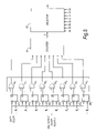
- FIG. 8 shows parts of another embodiment of the phase estimator
- FIG. 9 shows parts of a further embodiment of the phase estimator.
- FIG. 10 shows parts of a clock recovery circuit according to a second embodiment of the present invention.
- FIG. 1 shows parts of an example communications system with which the present invention may be used.
- three transmitters 10 , 12 , 14 each transmits a serial data signal.
- the transmitters operate on a time division multiplex basis, with each transmitter being allocated a window in which it may transmit a burst of data.
- the various data signals are combined in multiplexer 16 , transmitted over transmission channel 18 , and received by receiver 20 .
- the transmitters 10 , 12 , 14 are arranged such that each transmitter transmits a data signal at the same frequency as the other transmitters. However, due to differences in path length between the transmitters and the receiver, each data signal is received by the receiver with a difference phase.
- a clock and data recovery (CDR) circuit is provided, which recovers a clock signal from each data burst, and uses the clock signal to recover the data.
- FIG. 2 shows an example of the format of the data bursts transmitted by the transmitters 10 , 12 , 14 .
- each data burst comprises a four-byte header and a 53-byte payload containing the useful data.
- the header comprises a guard byte, two bytes with a predetermined pattern and a delimiter byte.
- the predetermined pattern consists of alternate ones and zeros, and is used to recover the clock signal.
- FIG. 3 shows parts of a previously considered clock and data recovery circuit.
- the circuit is a digital phase locked loop which is used to lock the phase of a clock signal to the phase of an incoming data signal.
- the clock and data recovery circuit comprises phase detector 22 , digital loop filter 24 , reference clock generator 25 , multiphase clock generator 26 and phase interpolator 28 .
- the reference clock generator 25 produces a reference clock signal which has a frequency which is the same as or very close to the frequency of the incoming data signal.
- the output of the reference clock generator 25 is fed to multiphase clock generator 26 .
- Multiphase clock generator 26 produces four multiphase clock signals which all have the same frequency, but with phases offset by 90°.
- the four multiphase clock signals are fed to phase interpolator 28 .
- Phase interpolator 26 receives the four multiphase clock signals, and a tap signal from the digital loop filter 24 .
- the tap signal is a six-bit signal indicating a desired phase of a clock signal (i.e. one of sixty four possible phases of the clock signal).
- the phase interpolator 26 mixes the four multiphase clock signals in accordance with the tap signal, to produce an output clock signal with the same frequency as the reference clock signal, but with a phase determined by the tap signal. The thus produced clock signal is fed to phase detector 22 .
- the phase detector 22 receives the clock signal and the incoming data signal, and produces an early/late signal which indicates whether the clock signal is early or late with respect to the data signal.
- the early/late signal is fed to digital loop filter 24 , which integrates the early/late signal over a number of bit periods and updates the tap signal to indicate the next phase of the clock signal.
- the tap signal is fed to the phase interpolator 26 which adjusts the phase of the clock signal in dependence thereon. In this way, the phase of the clock signal is locked to the phase of the data signal.
- the phase detector 22 in FIG. 3 obtains the early/late signal by sampling the data signal using various versions of the clock signal. One of these sampled data signals is output by the phase detector as the recovered data signal. Thus, in the circuit shown in FIG. 3 , it is not necessary to provide a separate latch for sampling the data signal.
- a problem with the circuit shown in FIG. 3 is that it may take a large number of cycles for the digital phased locked loop to lock on to the incoming data stream. For example, if the incoming data stream is at a frequency of 622 MHz, it may take hundreds or thousands of clock cycles before lock is achieved. This is due mainly to the latency of the loop, in particular due to the digital loop filter which may have several register stages and may operate at a lower frequency than that of the data stream (for example 78 MHz).
- FIG. 4 shows parts of a clock recovery circuit according to a first embodiment of the present invention.
- the clock recovery circuit comprises phase detector 30 , digital loop filter 32 , reference clock generator 34 , multiphase clock generator 36 , phase interpolator 38 , phase estimator 40 , switch 42 and control unit 44 .
- the phase detector 30 , digital loop filter 32 , reference clock generator 34 , multiphase clock generator 36 and phase interpolator 38 have essentially the same function as the corresponding parts shown in FIG. 3 , but with certain modifications as will be apparent from the following description.
- multiphase clock generator 36 receives a reference clock signal from reference clock generator 34 and produces a total of eight multiphase clock signals each having the same frequency as each other, but with evenly-spaced phases.
- Four clock signals with evenly spaced phases i.e. with spacings of 90°
- phase interpolator 38 for use in producing a clock signal with a phase determined by the tap signal at its input.
- Eight clock signals with evenly spaced phases are fed to phase estimator 40 .
- phase estimator 40 uses the eight clock signals at its input together with the incoming data signal to obtain an estimate of the desired phase of the clock signal.
- the clock recovery circuit of FIG. 4 is operable in one of two operation modes, fast mode and continuous mode, in dependence on a select signal output by control unit 44 .
- fast mode When in continuous mode the switch 42 selects the tap signal output from digital loop filter 32 and feeds this to the phase interpolator 38 .
- the clock recovery circuit functions in the same way as the clock recovery circuit described above with reference to FIG. 3 .
- phase estimator 40 When the clock recovery circuit is operating in fast mode, an estimate of the desired phase of the clock signal is produced by phase estimator 40 , and this estimate is selected by switch 42 and fed to phase interpolator 38 . The estimate is also fed to digital loop filter 32 , to update the tap signal which is produced by the filter.
- the phase estimator 40 is able to produce an estimate of the desired phase of the clock signal in a relatively short period of time, compared to the average time taken for the digital phase locked loop to lock onto the data signal.
- the digital phase locked loop can be brought quickly into a near-lock state. Once the initial estimate has been fed to the phase locked loop, the circuit is switched to continuous mode and final lock is achieved.
- the fast mode is normally selected when a new data burst is first received, and the continuous mode is normally selected once the initial estimate has been fed into the digital phase locked loop.
- fast mode could also be selected in other circumstances, for example if the digital phase locked loop lost lock part of the way through a data burst for some reason, or in dependence on the type of data signal.
- the tap signal output by the digital loop filter 32 is a six bit digital signal, which indicates which one of 64 possible phases the clock signal at the output of the phase interpolator should have.
- the output of the phase estimator 40 is also a six bit digital signal which can directly replace the output of the digital loop filter.
- FIG. 5 shows the main parts of the phase estimator 40 .
- the phase estimator 40 comprises eight-way sampler 46 , bit reversal detector 48 and selector 50 .
- the eight-way sampler 46 receives the eight multiphase clock signals and uses them to sample the incoming data signal at respective sampling points, to produce eight sampled data signals.
- the eight sampled data signals are fed to bit reversal detector 48 , which monitors each of the eight sampled data signals, and detects when a sampled data signal changes its state in comparison to the data signal which was sampled at the preceding sampling point. In this way it is determined at which sampling point a bit reversal occurs.
- Bit reversal detector 48 outputs a signal indicating the sampling point at which a bit reversal was determined to occur. This signal may either be a change in state on one of eight output lines as indicated in FIG. 5 , or it may be a three bit binary signal.
- the output of the bit reversal detector 48 is fed to selector 50 , which also receives eight six-bit tap signals.
- the selector 50 selects one of the eight tap signals in dependence on which sampling point was determined to have a bit reversal.
- Each of the eight tap signals is arranged to represent a phase which would be approximately the correct phase for the clock signal, if a bit reversal occurred at the corresponding sampling point.
- the selected tap signal is then fed to the switch 42 and digital loop filter 32 in FIG. 4 .
- FIG. 6 shows in more detail parts of the phase estimator 40 .
- the eight-way sampler comprises eight registers 60 1 to 60 8 and the bit reversal detector comprises eight EXOR gates 62 1 to 62 8 .
- Each of the eight registers 60 1 to 60 8 receives a respective one of the eight multiphase clock signals at its clock input, and receives the data signal at its data input. In this way, each of the registers 60 1 to 60 1 samples the data signal at a sampling point which is offset from that of the adjacent register.
- each register 60 1 to 60 8 is fed to a corresponding EXOR gate 62 1 to 62 8 .
- Each EXOR gate 62 1 to 62 8 also receives the output from the register having the preceding sampling point. When a register has the same output as the register having the preceding sampling point, the output of the corresponding EXOR gate is logic zero. However, if a register has an output which differs from that of the register having the preceding sampling point, then the output of the corresponding EXOR gate is logic one. In this way the outputs of the EXOR gates indicate which of the eight registers changed its state in comparison to the register having the preceding sampling point.
- the signals from the respective EXOR gates 62 1 to 62 8 are fed to the control inputs of selector 50 .
- Selector 50 also receives the eight tap signals, each of which is a one-of-sixty four tap signal in the same format as the tap signal output by digital loop filter 32 in FIG. 4 .
- the selector 50 selects one of the eight tap signals in dependence on which of the signals from the EXOR gates is logic one. In the example shown in FIG. 6 , if the output of EXOR gate 62 1 is logic one, then tap signal number 32 (i.e. phase number 32 out of 64 ) is selected by selector 50 ; if the output of EXOR gate 62 2 is logic one, then tap signal number 40 is selected by selector 50 ; and so forth.
- a sampling point at which a bit reversal occurs is considered to be at a data edge, and the centre of the data eye is taken to be approximately half a bit period away.
- an estimate of the desired phase of the clock signal can be obtained by adding half a bit period to the sampling point at which the bit reversal occurred.
- the eight tap signals which are input to the selector 50 are chosen to have the required offset (e.g. half a bit period) from the sampling point at which the bit reversal occurred, so that an estimate of the desired phase of the clock signal is produced at the output of the selector 50 .
- the same offset is also used by the phase locked loop when the circuit is operating in continuous mode.
- FIG. 7 shows an incoming serial data signal (RX serial data) which is at the start of a data burst.
- the data signal is sampled by eight multiphase clock signals, to give the sampled values shown. Due to their offset phases, the eight clock signals sample the data at regular intervals throughout a bit period, as indicated by the sampling points 0 to 7 .
- FIG. 7 also shows a select signal, which controls the switch 42 in FIG. 4 .
- the various clock signals start sampling the incoming data signal.
- the data is initially low, and so the sampled values are initially logic zero.
- the sampled values start to change from logic zero to logic one. This occurs at sampling point 1 , and so sampling point 1 is determined to be the sampling point at which a bit reversal occurred.
- the selector 50 in FIGS. 5 and 6 therefore selects the second of the eight tap signals at its input.
- the thus selected tap signal is fed by switch 42 in FIG. 4 to the phase interpolator 38 for use as an initial estimate of the desired phase of the clock signal.
- the select signal changes state, and the circuit is switched over to continuous mode.
- the tap signal from the digital loop filter 32 in FIG. 4 is fed to the phase interpolator 38 , and the phase locked loop locks onto the data signal.
- FIG. 8 shows parts of an alternative implementation of the phase estimator 40 .
- the phase estimator shown in FIG. 8 comprises eight registers 60 1 to 60 8 and eight EXOR gates 62 1 to 62 8 , which are the same as the corresponding parts in FIG. 6 .
- the phase estimator of FIG. 8 also comprises a counter 64 , which counts the number of times each of the EXOR gates produces a logic one signal.
- the counter 64 produces a three bit signal which indicates which one of the eight EXOR gates produced the most logic one signals. This three bit signal is fed to selector 66 , which selects one of eight taps signals in dependence on the value of the three bit signal.
- the phase estimator shown in FIG. 8 takes advantage of the fact that a number of data edges may be available for locking the clock signal to the incoming data. For example, if the data format shown in FIG. 2 is used, up to sixteen data transitions may be available. By counting the number of bit reversals associated with each sampling point, and determining which sampling point has the most bit reversals, a better estimate of the correct phase of the clock signal may be obtained, and spurious results may be avoided.
- the counter 64 may operate over a predetermined number of cycles, in which case its output will indicate which of the EXOR gates produced a logic one signal the most times during those cycles.
- the counter may be arranged to output a signal once one of the EXOR gates has produced a predetermined number of logic one signals.
- the selector 66 is arranged to select one of the eight tap signals once the final output from the counter 64 is produced.
- the counter 64 may also be arranged to output a “running total”, which indicates which of the EXOR gates has produced a logic one signal the most times since, for example, the start of a data burst. This can allow an initial estimate of the desired phase of the clock signal to be made available as soon as the first data edge has been detected, and this estimate to be updated as more data edges are detected. Once a certain number of data edges have been detected, the counter may operate as a “sliding window”, in which old results are discarded. In this implementation, the output of the counter 64 may indicate which of the EXOR gates has produced a logic one signal the most times, for example, during a predetermined number of clock cycles, or based on a predetermined number of detected data edges.
- the counter 64 is arranged to output a signal which is based on an average of the logic one signals which appear at its inputs.
- FIG. 9 shows parts of another possible implementation of the phase estimator 40 .
- the phase estimator shown in FIG. 9 comprises eight registers 60 1 to 60 8 and eight EXOR gates 62 1 to 62 8 , which are the same as the corresponding parts in FIGS. 6 and 8 .
- the phase estimator in this implementation also comprises stepper 68 and selector 70 .
- the stepper 68 receives the eight input signals from the EXOR gates 62 1 to 62 8 , and outputs a three bit signal which has a value corresponding to one of the eight input signals.
- the three bit signal output by the stepper 68 is used to select one of eight tap signals input to the selector 70 .
- the stepper 68 changes its output so as to step towards the value that does correspond to the input that is currently at logic one.
- the stepper 68 may step its output by, for example, one value with each clock cycle, or by more than one value. This arrangement can allow an estimate of the desired phase of the clock signal to be produced quickly, while allowing the effects of spuriously detected data edges to be reduced.
- the stepper 68 has an output which corresponds to an arbitrary one of the eight input signals. If desired, following initialisation, the output of the stepper may first be set to correspond to the input which is at logic one once the first data edge has been detected. Alternatively the output of the stepper may simply be allowed to step towards its input at all times. Assuming that the input to the stepper remains constant and the output of the stepper steps by one value with each clock cycle, then it will take a maximum of four clock cycles for the output to correspond to the input.
- FIG. 10 shows parts of a clock recovery circuit according to another embodiment of the present invention.
- the clock recovery circuit in this embodiment comprises reference clock generator 80 , multiphase clock generator 82 , phase interpolator 84 , phase estimator 86 and latch 88 .
- the clock recovery circuit shown in FIG. 10 differs from that shown in FIG. 4 in that no digital phase locked loop is provided. Instead, the phase estimator 86 is used to continually set the phase of the clock signal output by the phase interpolator 84 . The thus produced clock signal latches the data signal in latch 88 to produce the recovered data signal.
- the phase estimator 86 may be in any of the forms described above with reference to the first embodiment. However, since the number of possible phases is determined by the phase estimator itself, rather than the digital loop filter 32 in FIG. 4 , the output of the phase estimator is a 1-of-n signal, where n is the number of multiphase clock signals input to the phase estimator. Thus the inputs to the selector (such as selector 50 in FIG. 6 , or selector 66 in FIG. 8 , or selector 70 in FIG. 9 ) are chosen accordingly. In the example shown in FIG. 10 , eight multiphase clock signals are input to the phase estimator 86 and the output of the phase estimator is a three bit (1-of-8) signal. However, the phase estimator could use a larger number of multiphase clock signals if desired, in order to set the phase of the clock signal with smaller gradations.
- phase estimator in the embodiments described above uses eight reference clock signals to sample the data, any desired number of reference clock signals having appropriately spaced phases could be used, and the phases need not be evenly spaced.
- tap signals other than 1 of 64 tap signals could be used.
- the tap signals may be encoded, for example using Gray coding or thermometer coding or any other appropriate form of coding. Where appropriate, an encoder may be included in the circuitry in order to produce the required encoding.
- phase interpolator is used to produce the clock signal, but it will be appreciated that any other appropriate technique could be used to produce the clock signal. For example, sixty four multiphase clock signals (or some other number, depending on the number of possible values of the tap signal) could be produced, and one of those signals could be selected as the clock signal.
- the clock signal may have any appropriate phase offset with respect to the data signal, and this may be preset, or adjustable.
- a separate latch may be provided for sampling the data signal, and the clock signal applied to that latch may have an adjustable offset.
Abstract
Description
-
- sampling means for sampling the data signal at a plurality of sampling points;
- bit reversal detecting means for determining a sampling point at which the data signal changes state;
- selecting means for selecting a phase from amongst a plurality of candidate phases based on a sampling point at which the data signal is determined to change state; and
- setting means for setting the phase of the clock signal in dependence on the selected phase.
-
- sampling the data signal at a plurality of sampling points;
- determining a sampling point at which the data signal changes state;
- selecting a phase from amongst a plurality of candidate phases based on a sampling point at which the data signal is determined to change state; and
- setting the phase of the clock signal in dependence on the selected phase.
-
- a sampler which samples the data signal at a plurality of sampling points;
- a bit reversal detector which determines a sampling point at which the data signal changes state;
- a selector which selects a phase from amongst a plurality of candidate phases based on a sampling point at which the data signal is determined to change state; and
- a phase setting unit which sets the phase of the clock signal in dependence on the selected phase.
Claims (21)
Applications Claiming Priority (2)
| Application Number | Priority Date | Filing Date | Title |
|---|---|---|---|
| GB0204497A GB2385728B (en) | 2002-02-26 | 2002-02-26 | Clock recovery circuitry |
| GB0204497.2 | 2002-02-26 |
Publications (2)
| Publication Number | Publication Date |
|---|---|
| US20030161430A1 US20030161430A1 (en) | 2003-08-28 |
| US7577226B2 true US7577226B2 (en) | 2009-08-18 |
Family
ID=9931817
Family Applications (1)
| Application Number | Title | Priority Date | Filing Date |
|---|---|---|---|
| US10/315,088 Expired - Fee Related US7577226B2 (en) | 2002-02-26 | 2002-12-10 | Clock recovery circuitry |
Country Status (4)
| Country | Link |
|---|---|
| US (1) | US7577226B2 (en) |
| JP (1) | JP3955824B2 (en) |
| DE (1) | DE10301130B4 (en) |
| GB (1) | GB2385728B (en) |
Cited By (7)
| Publication number | Priority date | Publication date | Assignee | Title |
|---|---|---|---|---|
| US20080193125A1 (en) * | 2007-01-16 | 2008-08-14 | Broadlight Ltd. | Apparatus and method for measuring the quality of burst signals and performing optical line diagnostics |
| US20110029803A1 (en) * | 2008-04-04 | 2011-02-03 | Nxp B.V. | Clock recovery of serial data signal |
| US20120063296A1 (en) * | 2010-09-10 | 2012-03-15 | Broadcom Corporation | Systems and Methods for Providing a Dual-Master Mode in a Synchronous Ethernet Environment |
| US20140334581A1 (en) * | 1998-11-25 | 2014-11-13 | Texas Instruments Incorporated | Plural circuit selection using role reversing control inputs |
| US20150001404A1 (en) * | 2011-12-06 | 2015-01-01 | The Board Of Trustees Of The Leland Stanford Junior University | Time-based digitizer for pet photodetector |
| US9036729B2 (en) | 2013-02-19 | 2015-05-19 | Avago Technologies General Ip (Singapore) Pte. Ltd. | Code forwarding and clock generation for transmitter repeaters |
| US20170116954A1 (en) * | 2015-10-22 | 2017-04-27 | Samsung Electronics Co., Ltd. | Clock and data recovery circuit detecting unlock of output of phase locked loop |
Families Citing this family (30)
| Publication number | Priority date | Publication date | Assignee | Title |
|---|---|---|---|---|
| US8155236B1 (en) | 2002-06-21 | 2012-04-10 | Netlogic Microsystems, Inc. | Methods and apparatus for clock and data recovery using transmission lines |
| US7231008B2 (en) * | 2002-11-15 | 2007-06-12 | Vitesse Semiconductor Corporation | Fast locking clock and data recovery unit |
| WO2004098120A1 (en) * | 2003-05-01 | 2004-11-11 | Mitsubishi Denki Kabushiki Kaisha | Clock data recovery circuit |
| US20040223567A1 (en) * | 2003-05-09 | 2004-11-11 | Ming-Kang Liu | Clock recovery system |
| US20040223568A1 (en) * | 2003-05-09 | 2004-11-11 | Ming-Kang Liu | Phase sampling determination system |
| TWI226774B (en) * | 2003-10-15 | 2005-01-11 | Via Tech Inc | Clock and data recovery circuit |
| ATE358925T1 (en) * | 2004-01-19 | 2007-04-15 | Vitesse Semiconductor Corp | QUICK LOCKING CLOCK AND DATA RECOVERY UNIT |
| WO2005122460A1 (en) * | 2004-06-04 | 2005-12-22 | Opelcomm, Inc. | Clock recovery system and phase sampling determination system |
| DE602004026195D1 (en) * | 2004-10-21 | 2010-05-06 | Hewlett Packard Development Co | Serial bus system |
| US7532697B1 (en) | 2005-01-27 | 2009-05-12 | Net Logic Microsystems, Inc. | Methods and apparatus for clock and data recovery using a single source |
| US7693243B2 (en) * | 2005-09-26 | 2010-04-06 | Via Technologies, Inc. | Method and circuit for timing recovery |
| US7432750B1 (en) | 2005-12-07 | 2008-10-07 | Netlogic Microsystems, Inc. | Methods and apparatus for frequency synthesis with feedback interpolation |
| US7724857B2 (en) * | 2006-03-15 | 2010-05-25 | Agere Systems Inc. | Method and apparatus for improving linearity in clock and data recovery systems |
| DE102006020107B3 (en) * | 2006-04-29 | 2007-10-25 | Infineon Technologies Ag | Data receiver for use in serial data transmission system of e.g. semiconductor memory, has sampling unit connected with data signal input for sampling data signal amplitude and amplifying sampled data signal amplitude to specific value |
| EP1903712B1 (en) * | 2006-09-25 | 2012-11-21 | Silicon Image, Inc. | Signal interleaving for serial clock and data recovery |
| US8243869B2 (en) * | 2006-11-28 | 2012-08-14 | Broadlight Ltd. | Burst mode clock and data recovery circuit and method |
| JP4425945B2 (en) * | 2007-03-20 | 2010-03-03 | 富士通株式会社 | Transponder unit, transponder unit control device, transponder unit control method, and transponder unit control program |
| US7728636B2 (en) * | 2007-08-14 | 2010-06-01 | Qimonda Ag | Clock signal synchronizing device with inherent duty-cycle correction capability |
| US7532135B1 (en) * | 2007-11-26 | 2009-05-12 | Broadcom Corporation | Dual purpose serializer/de-serializer for point-to-point and point-to-multipoint communication |
| US7929644B2 (en) * | 2008-02-01 | 2011-04-19 | Panasonic Corporation | Instant-acquisition clock and data recovery systems and methods for serial communications links |
| TWI358906B (en) * | 2008-08-15 | 2012-02-21 | Ind Tech Res Inst | Burst-mode clock and data recovery circuit using p |
| US8520744B2 (en) | 2010-03-19 | 2013-08-27 | Netlogic Microsystems, Inc. | Multi-value logic signaling in multi-functional circuits |
| US8638896B2 (en) * | 2010-03-19 | 2014-01-28 | Netlogic Microsystems, Inc. | Repeate architecture with single clock multiplier unit |
| US8423814B2 (en) | 2010-03-19 | 2013-04-16 | Netlogic Microsystems, Inc. | Programmable drive strength in memory signaling |
| US8537949B1 (en) | 2010-06-30 | 2013-09-17 | Netlogic Microsystems, Inc. | Systems, circuits and methods for filtering signals to compensate for channel effects |
| US8494377B1 (en) | 2010-06-30 | 2013-07-23 | Netlogic Microsystems, Inc. | Systems, circuits and methods for conditioning signals for transmission on a physical medium |
| US8483344B2 (en) | 2011-06-13 | 2013-07-09 | Stephen C. Dillinger | Fast lock serializer-deserializer (SERDES) architecture |
| TWI486780B (en) * | 2013-08-13 | 2015-06-01 | Phison Electronics Corp | Connecting interface unit and memory storage device |
| CN104363016B (en) * | 2014-10-17 | 2018-03-13 | 青岛歌尔声学科技有限公司 | A kind of clock data recovery circuit and clock and data recovery method |
| US11736268B2 (en) | 2021-11-04 | 2023-08-22 | L3Harris Technologies, Inc. | Clock recovery |
Citations (11)
| Publication number | Priority date | Publication date | Assignee | Title |
|---|---|---|---|---|
| US4630283A (en) * | 1985-07-17 | 1986-12-16 | Rca Corporation | Fast acquisition burst mode spread spectrum communications system with pilot carrier |
| US4672639A (en) * | 1984-05-24 | 1987-06-09 | Kabushiki Kaisha Toshiba | Sampling clock pulse generator |
| GB2240241A (en) | 1990-01-18 | 1991-07-24 | Plessey Co Plc | Data transmission systems |
| US5187479A (en) | 1991-09-30 | 1993-02-16 | Am International Incorporated | Backlash compensation circuit for use with an incremental encoder |
| US5315299A (en) | 1992-02-14 | 1994-05-24 | Nissan Motor Co., Ltd. | Multiplex data communicating apparatus applicable to automotive vehicle |
| EP0746111A1 (en) | 1995-05-31 | 1996-12-04 | Nec Corporation | Phase-locked loop for clock recovery |
| EP0952568A1 (en) | 1998-04-23 | 1999-10-27 | THOMSON multimedia | Process of clock recovery during the sampling of digital-type signals |
| US5977822A (en) | 1998-04-04 | 1999-11-02 | Sigmatel, Inc. | Method and apparatus of pulse position demodulation |
| US6125157A (en) * | 1997-02-06 | 2000-09-26 | Rambus, Inc. | Delay-locked loop circuitry for clock delay adjustment |
| US6247138B1 (en) * | 1997-06-12 | 2001-06-12 | Fujitsu Limited | Timing signal generating circuit, semiconductor integrated circuit device and semiconductor integrated circuit system to which the timing signal generating circuit is applied, and signal transmission system |
| US20010026179A1 (en) | 2000-03-24 | 2001-10-04 | Takanori Saeki | Clock control circuit and clock control method |
-
2002
- 2002-02-26 GB GB0204497A patent/GB2385728B/en not_active Expired - Fee Related
- 2002-12-10 US US10/315,088 patent/US7577226B2/en not_active Expired - Fee Related
-
2003
- 2003-01-14 DE DE10301130A patent/DE10301130B4/en not_active Expired - Fee Related
- 2003-01-17 JP JP2003009751A patent/JP3955824B2/en not_active Expired - Fee Related
Patent Citations (11)
| Publication number | Priority date | Publication date | Assignee | Title |
|---|---|---|---|---|
| US4672639A (en) * | 1984-05-24 | 1987-06-09 | Kabushiki Kaisha Toshiba | Sampling clock pulse generator |
| US4630283A (en) * | 1985-07-17 | 1986-12-16 | Rca Corporation | Fast acquisition burst mode spread spectrum communications system with pilot carrier |
| GB2240241A (en) | 1990-01-18 | 1991-07-24 | Plessey Co Plc | Data transmission systems |
| US5187479A (en) | 1991-09-30 | 1993-02-16 | Am International Incorporated | Backlash compensation circuit for use with an incremental encoder |
| US5315299A (en) | 1992-02-14 | 1994-05-24 | Nissan Motor Co., Ltd. | Multiplex data communicating apparatus applicable to automotive vehicle |
| EP0746111A1 (en) | 1995-05-31 | 1996-12-04 | Nec Corporation | Phase-locked loop for clock recovery |
| US6125157A (en) * | 1997-02-06 | 2000-09-26 | Rambus, Inc. | Delay-locked loop circuitry for clock delay adjustment |
| US6247138B1 (en) * | 1997-06-12 | 2001-06-12 | Fujitsu Limited | Timing signal generating circuit, semiconductor integrated circuit device and semiconductor integrated circuit system to which the timing signal generating circuit is applied, and signal transmission system |
| US5977822A (en) | 1998-04-04 | 1999-11-02 | Sigmatel, Inc. | Method and apparatus of pulse position demodulation |
| EP0952568A1 (en) | 1998-04-23 | 1999-10-27 | THOMSON multimedia | Process of clock recovery during the sampling of digital-type signals |
| US20010026179A1 (en) | 2000-03-24 | 2001-10-04 | Takanori Saeki | Clock control circuit and clock control method |
Non-Patent Citations (1)
| Title |
|---|
| "High-Speed Clock & Data Recovery Macro for Data Transfer at 622 Mbits/sec", Fujitsu Spectrum, No. 123, Jun. 2001, pp. 3-6. |
Cited By (12)
| Publication number | Priority date | Publication date | Assignee | Title |
|---|---|---|---|---|
| US20140334581A1 (en) * | 1998-11-25 | 2014-11-13 | Texas Instruments Incorporated | Plural circuit selection using role reversing control inputs |
| US8964918B2 (en) * | 1998-11-25 | 2015-02-24 | Texas Instruments Incorporated | IC first, second communication circuits each with three communication states |
| US20080193125A1 (en) * | 2007-01-16 | 2008-08-14 | Broadlight Ltd. | Apparatus and method for measuring the quality of burst signals and performing optical line diagnostics |
| US7925156B2 (en) * | 2007-01-16 | 2011-04-12 | Broadlight, Ltd. | Apparatus and method for measuring the quality of burst signals and performing optical line diagnostics |
| US20110029803A1 (en) * | 2008-04-04 | 2011-02-03 | Nxp B.V. | Clock recovery of serial data signal |
| US20120063296A1 (en) * | 2010-09-10 | 2012-03-15 | Broadcom Corporation | Systems and Methods for Providing a Dual-Master Mode in a Synchronous Ethernet Environment |
| US8619755B2 (en) * | 2010-09-10 | 2013-12-31 | Broadcom Corporation | Systems and methods for providing a dual-master mode in a synchronous ethernet environment |
| US20150001404A1 (en) * | 2011-12-06 | 2015-01-01 | The Board Of Trustees Of The Leland Stanford Junior University | Time-based digitizer for pet photodetector |
| US9244179B2 (en) * | 2011-12-06 | 2016-01-26 | The Board Of Trustees Of The Leland Stanford Junior University | Time-based digitizer for PET photodetector |
| US9036729B2 (en) | 2013-02-19 | 2015-05-19 | Avago Technologies General Ip (Singapore) Pte. Ltd. | Code forwarding and clock generation for transmitter repeaters |
| US20170116954A1 (en) * | 2015-10-22 | 2017-04-27 | Samsung Electronics Co., Ltd. | Clock and data recovery circuit detecting unlock of output of phase locked loop |
| US9959835B2 (en) * | 2015-10-22 | 2018-05-01 | Samsung Electronics Co., Ltd. | Clock and data recovery circuit detecting unlock of output of phase locked loop |
Also Published As
| Publication number | Publication date |
|---|---|
| DE10301130B4 (en) | 2006-11-02 |
| GB2385728A (en) | 2003-08-27 |
| US20030161430A1 (en) | 2003-08-28 |
| JP2003258782A (en) | 2003-09-12 |
| GB0204497D0 (en) | 2002-04-10 |
| JP3955824B2 (en) | 2007-08-08 |
| GB2385728B (en) | 2006-07-12 |
| DE10301130A1 (en) | 2003-09-18 |
Similar Documents
| Publication | Publication Date | Title |
|---|---|---|
| US7577226B2 (en) | Clock recovery circuitry | |
| US11063741B2 (en) | Phase control block for managing multiple clock domains in systems with frequency offsets | |
| US7315596B2 (en) | Interpolator based clock and data recovery (CDR) circuit with digitally programmable BW and tracking capability | |
| US4821297A (en) | Digital phase locked loop clock recovery scheme | |
| EP2183674B1 (en) | Transmitter and receiver connected through a serial channel | |
| US7027544B2 (en) | Data clocked recovery circuit | |
| US7349509B2 (en) | Multi rate clock data recovery based on multi sampling technique | |
| US7450677B2 (en) | Clock and data recovery apparatus and method thereof | |
| JPH08163117A (en) | Bit phase synchronizing circuit | |
| US9966994B2 (en) | Apparatus and methods for burst mode clock and data recovery for high speed serial communication links | |
| US6002731A (en) | Received-data bit synchronization circuit | |
| US5717728A (en) | Data/clock recovery circuit | |
| US9887831B2 (en) | Clock data recovery circuit, integrated circuit including the same, and clock data recovery method | |
| US20050135518A1 (en) | Improvements to data recovery circuits using oversampling for isi compensation | |
| US20040096016A1 (en) | Fast locking clock and data recovery unit | |
| EP1113616B1 (en) | Method for recovering a clock signal in a telecommunications system and circuit thereof | |
| US6990122B2 (en) | Synchronism phase-switching circuit for the recovery of received data | |
| US20030014683A1 (en) | Receiver with automatic skew compensation | |
| US6438155B1 (en) | Decoding chip streams | |
| EP1386441B1 (en) | Receiver with recovery circuit using oversampling and majority decision | |
| US6011808A (en) | Redundant codes for clock recovery in serial links | |
| EP1545047B1 (en) | Improvements to data recovery circuits using oversampling for ISI compensation | |
| EP1076435A1 (en) | A detector for detecting timing in a data flow |
Legal Events
| Date | Code | Title | Description |
|---|---|---|---|
| AS | Assignment |
Owner name: FUJITSU LIMITED, JAPAN Free format text: ASSIGNMENT OF ASSIGNORS INTEREST;ASSIGNOR:SOU, ANTONY;REEL/FRAME:013560/0711 Effective date: 20021114 |
|
| AS | Assignment |
Owner name: FUJITSU MICROELECTRONICS LIMITED,JAPAN Free format text: ASSIGNMENT OF ASSIGNORS INTEREST;ASSIGNOR:FUJITSU LIMITED;REEL/FRAME:021977/0219 Effective date: 20081104 Owner name: FUJITSU MICROELECTRONICS LIMITED, JAPAN Free format text: ASSIGNMENT OF ASSIGNORS INTEREST;ASSIGNOR:FUJITSU LIMITED;REEL/FRAME:021977/0219 Effective date: 20081104 |
|
| STCF | Information on status: patent grant |
Free format text: PATENTED CASE |
|
| FEPP | Fee payment procedure |
Free format text: PAYOR NUMBER ASSIGNED (ORIGINAL EVENT CODE: ASPN); ENTITY STATUS OF PATENT OWNER: LARGE ENTITY |
|
| AS | Assignment |
Owner name: FUJITSU SEMICONDUCTOR LIMITED, JAPAN Free format text: CHANGE OF NAME;ASSIGNOR:FUJITSU MICROELECTRONICS LIMITED;REEL/FRAME:024982/0245 Effective date: 20100401 |
|
| FPAY | Fee payment |
Year of fee payment: 4 |
|
| AS | Assignment |
Owner name: SOCIONEXT INC., JAPAN Free format text: ASSIGNMENT OF ASSIGNORS INTEREST;ASSIGNOR:FUJITSU SEMICONDUCTOR LIMITED;REEL/FRAME:035508/0337 Effective date: 20150302 |
|
| FPAY | Fee payment |
Year of fee payment: 8 |
|
| FEPP | Fee payment procedure |
Free format text: MAINTENANCE FEE REMINDER MAILED (ORIGINAL EVENT CODE: REM.); ENTITY STATUS OF PATENT OWNER: LARGE ENTITY |
|
| LAPS | Lapse for failure to pay maintenance fees |
Free format text: PATENT EXPIRED FOR FAILURE TO PAY MAINTENANCE FEES (ORIGINAL EVENT CODE: EXP.); ENTITY STATUS OF PATENT OWNER: LARGE ENTITY |
|
| STCH | Information on status: patent discontinuation |
Free format text: PATENT EXPIRED DUE TO NONPAYMENT OF MAINTENANCE FEES UNDER 37 CFR 1.362 |
|
| FP | Lapsed due to failure to pay maintenance fee |
Effective date: 20210818 |