US7656968B2 - Radio receiver, system on a chip integrated circuit and methods for use therewith - Google Patents
Radio receiver, system on a chip integrated circuit and methods for use therewith Download PDFInfo
- Publication number
- US7656968B2 US7656968B2 US11/287,571 US28757105A US7656968B2 US 7656968 B2 US7656968 B2 US 7656968B2 US 28757105 A US28757105 A US 28757105A US 7656968 B2 US7656968 B2 US 7656968B2
- Authority
- US
- United States
- Prior art keywords
- signal
- digital
- digital clock
- frequency
- integrated circuit
- Prior art date
- Legal status (The legal status is an assumption and is not a legal conclusion. Google has not performed a legal analysis and makes no representation as to the accuracy of the status listed.)
- Expired - Fee Related, expires
Links
Images


Classifications
-
- H—ELECTRICITY
- H04—ELECTRIC COMMUNICATION TECHNIQUE
- H04B—TRANSMISSION
- H04B15/00—Suppression or limitation of noise or interference
- H04B15/02—Reducing interference from electric apparatus by means located at or near the interfering apparatus
-
- H—ELECTRICITY
- H04—ELECTRIC COMMUNICATION TECHNIQUE
- H04B—TRANSMISSION
- H04B2215/00—Reducing interference at the transmission system level
- H04B2215/064—Reduction of clock or synthesizer reference frequency harmonics
- H04B2215/065—Reduction of clock or synthesizer reference frequency harmonics by changing the frequency of clock or reference frequency
Definitions
- Controllable phase locked loop and method for producing an output oscillation for use therewith having Ser. No. 11/126,553, filed on May 11, 2005;
- Controllable phase locked loop via adjustable delay and method for producing an output oscillation for use therewith having Ser. No. 11/153,144, filed on Jun. 15, 2005;
- the present invention relates to radio receivers used in devices such as system on a chip integrated circuits, and related methods.
- Radio receivers can be implemented in integrated circuits that can provide an entire receiver front end on a single chip.
- One concern in the design of these circuits is the amount of noise that is produced.
- Digital circuit designs can reduce the amount of analog noise, such as thermal noise that is introduced.
- other sources of noise can be present.
- the presence of periodic switching events and other signals within the frequency band of the input circuitry can cause undesirable spurs from switching events.
- Digital clocks and their harmonics also produce tones that can degrade performance in the analog circuitry.
- FIG. 1 presents a pictorial diagram of a handheld audio system in accordance with an embodiment of the present invention.
- FIG. 2 presents a schematic block diagram of a radio receiver in accordance with an embodiment of the present invention.
- FIG. 3 presents a schematic block diagram of a radio receiver in accordance with an alternative embodiment of the present invention.
- FIG. 4 presents a combination block diagram and schematic diagram of a radio receiver in accordance with an embodiment of the present invention.
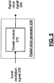
- FIG. 5 presents a block diagram representation of a digital clock signal generator in accordance with an embodiment of the present invention.
- FIG. 6 presents a block diagram of a method in accordance with an embodiment of the present invention.
- FIG. 7 presents a block diagram of a method in accordance with an embodiment of the present invention.
- FIG. 8 presents a block diagram of a method in accordance with an embodiment of the present invention.
- FIG. 9 presents a block diagram of a method in accordance with an embodiment of the present invention.
- the embodiments of the present invention yield several advantages over the prior art.
- the present invention details an implementation for an efficient architecture for receiving a radio signal.
- a digital clock frequency varies with the carrier frequency of a received signal, and is controlled so that its fundamental and harmonics do not interfere with the processing of the received signal. This advantage as well as others will apparent to one skilled in the art when presented the disclosure herein.
- FIG. 1 presents a pictorial diagram of a handheld audio system in accordance with an embodiment of the present invention.
- a handheld audio system 80 is shown that receives a radio signal that carries at least one composite audio channel that includes right and left channel stereo audio signals.
- the radio signal includes one or more of a broadcast frequency modulated (FM) radio signal, a broadcast amplitude modulated (AM) radio signal, an in-band on-channel (IBOC) digital radio signal, a Bluetooth signal, a broadcast satellite radio signal, and a broadcast cable signal.
- FM broadcast frequency modulated
- AM broadcast amplitude modulated
- IBOC in-band on-channel
- the handheld audio system 80 produces an audio output for a user by means of headphones 82 or other speaker systems.
- the handheld audio system 80 can optionally process stored MP3 files, stored WMA files, and/or other stored digital audio files to produce an audio output for the user.
- the handheld audio system may also include video features as well.
- Handheld audio system 80 includes a radio receiver and/or one or more integrated circuits (ICs) that implement the features and functions in accordance with one or more embodiments of the present invention that are discussed herein.
- ICs integrated circuits
- FIG. 2 presents a schematic block diagram of a radio receiver in accordance with an embodiment of the present invention.
- radio receiver 10 is presented that includes a radio signal decoder integrated circuit 150 that includes an analog front end 175 , digital clock generator 238 , digital section 225 and/or corresponding methods in accordance with FIGS. 3-9 , and a digital audio processing integrated circuit 100 .
- the radio signal decoder integrated circuit 150 is operably coupled to a reference oscillator circuit 230 and an antenna structure 34 .
- the reference oscillation circuit 230 is operably coupled to a crystal and produces therefrom a reference oscillation 232 and a system clock 22 that is provided to digital audio processing IC 100 .
- the antenna structure 34 includes an antenna, a plurality of capacitors and an inductor coupled as shown.
- the received radio signal 16 is provided from the antenna structure 34 to the radio signal decoder integrated circuit 150 .
- the radio signal decoder integrated circuit 150 converts the received radio signal 16 into left and right channel signals 18 .
- the digital audio processing integrated circuit 100 via a DC-DC converter, generates an input/output (I/O) dependent supply voltage 24 - 1 and an integrated circuit (IC) dependent voltage 24 - 2 that are supplied to the radio signal decoder IC 150 .
- the I/O dependent voltage 24 - 1 is dependent on the supply voltage required for input/output interfacing of the radio signal decoder IC and/or the digital audio processing IC 14 (e.g., 3.3 volts) and the IC dependent voltage 24 - 2 is dependent on the IC process technology used to produce integrated circuits 150 and 100 .
- the digital audio processing integrated circuit 100 further includes a processing module that may be a single processing device or a plurality of processing devices.
- Such a processing device may be a microprocessor, micro-controller, digital signal processor, microcomputer, central processing unit, field programmable gate array, programmable logic device, state machine, logic circuitry, analog circuitry, digital circuitry, and/or any device that manipulates signals (analog and/or digital) based on operational instructions.
- the memory may be a single memory device or a plurality of memory devices.
- Such a memory device may be a read-only memory, random access memory, volatile memory, non-volatile memory, static memory, dynamic memory, flash memory, cache memory, and/or any device that stores digital information.
- the memory when the processing module implements one or more of its functions via a state machine, analog circuitry, digital circuitry, and/or logic circuitry, the memory storing the corresponding operational instructions may be embedded within, or external to, the circuitry comprising the state machine, analog circuitry, digital circuitry, and/or logic circuitry. Further note that, the memory stores, and the processing module executes, operational instructions corresponding to at least some of the steps and/or functions illustrated in the Figures that follow.
- the interface between the integrated circuits 150 and 100 further includes a bi-directional interface 36 .
- Such an interface may be a serial interface for the integrated circuits 150 and 100 to exchange control data and/or other type of data.
- the bi-directional interface 36 may be one or more serial communication paths that are in accordance with the I 2 C serial transmission protocol.
- other serial transmission protocols may be used for the bi-directional interface 36 and the bi-directional interface 36 may include one or more serial transmission paths.
- radio signal decoder IC 150 is a system on a chip integrated circuit that operates as follows.
- Analog front end 175 receives received radio signal 16 having a plurality of channel signals, each of the plurality of channel signals being modulated at one of a corresponding plurality of carrier frequencies.
- Analog front end 175 is operable to convert a selected one of the plurality of channel signals into a digital signal 212 .
- Digital clock generator 238 generates a digital clock signal 240 at a digital clock frequency that varies based on the selected one of the plurality of channel signals.
- Digital section 225 is operably coupled to the analog front end 175 , and converts the digital signal 212 into at least one audio signal, such as left and right channel signals 18 , that correspond to the selected one of the plurality of channels, based on the digital clock signal 212 .
- the digital clock frequency, and the harmonics that are created at integer multiples of the digital clock frequency, are not substantially equal to the carrier frequency of the selected one of the plurality of channel signals.
- FIG. 3 presents a schematic block diagram of a radio receiver in accordance with an alternative embodiment of the present invention.
- a schematic block diagram of a radio receiver 11 is presented that includes the functionality of radio receiver 10 presented in an alternative system on a chip configuration.
- the functionality of radio signal decoder IC 150 and digital audio processing IC 100 are incorporated into a single integrated circuit, radio receiver IC 50 .
- radio receiver IC 50 includes analog front end 175 , digital clock generator 238 , as described in conjunction with FIG. 2 .
- a channel selector 260 produces a control signal 250 that corresponds to the selected one of the plurality of channels.
- a local oscillator 234 is operably coupled to the analog front end 175 and a reference oscillation 232 , for generating a local oscillation signal 236 based on the control signal 250 .
- the digital clock frequency is controlled so as to continue this advantageous relationship between the digital clock frequency and the new carrier frequency.
- handheld audio system 11 implements one or more of the features and functions of other embodiments of the present invention described in conjunction with FIGS. 1-9 .
- FIG. 4 presents a combination block diagram and schematic diagram of a radio receiver in accordance with an embodiment of the present invention.
- a radio receiver 55 receives a received radio signal 200 that includes a plurality of broadcast FM channel signals, each of the plurality of channel signals being modulated at one of a corresponding plurality of carrier frequencies.
- Reference oscillator 230 produces a reference oscillation 232 that is transformed by local oscillator 234 into a local oscillation signal 236 at a local oscillation frequency.
- a channel selector 260 produces control signal 250 that selects the local oscillation frequency for local oscillator 234 corresponding to a selection of one of the plurality of channels.
- local oscillator 234 includes a phase locked loop circuit for producing a selected local oscillation frequency based on the selected one of the plurality of channels.
- Low noise amplifier 202 produces a amplified radio signal 204 that is sampled and mixed with the local oscillation signal 236 by mixing module 206 to form a discrete time IF signal 208 at an intermediate frequency.
- the gain at which the low noise amplifier 202 amplifies the receive signal 200 is dependent on the magnitude of the received radio signal 200 and an automatic gain control circuit.
- IF signal 208 is a modulated signal and if the local oscillation signal 236 has an effective frequency (when considering the sample rate) that matches the frequency of the selected channel, the IF signal 208 will have a carrier frequency of approximately zero.
- the IF signal 208 will have a carrier frequency based on the difference between the carrier frequency of the selected channel and the effective frequency of local oscillation 236 .
- the carrier frequency of the IF signal 208 may range from 0 hertz to one megahertz or more.
- Analog to digital converter (ADC) module 210 converts the IF signal 208 into a digital signal 212 , based on clock signal 240 .
- digital signal 212 may or may not be down-converted to baseband.
- Programmable decimation filter 214 converts the digital signal 212 into a digital downsampled (DS) signal 216 , in response to control signal 250 .
- Digital clock signal 240 is a variable frequency clock and varies as a function of local oscillation signal 236 .
- programmable decimation filter 214 adjusts to produce digital downsampled signal 216 at a roughly constant output rate so that channel filter 218 , a digital filter that provides channel separation and produces filtered signal 220 , can employ constant coefficients.
- FM signal lock and decoding module 222 tracks the FM signal via the 19 kHz pilot signal and produces audio channel signals 224 , such as left and right channel signals 18 .
- received radio signal 200 is a frequency modulated (FM) broadcast signal that includes a plurality of channels that are spaced 200 kHz apart in the range of 76 MHz to 108 MHz.
- FM frequency modulated
- Channel selector 260 generates a control signal 250 that includes a 7 bit signal that commands local oscillator 234 to produce a 400 MHz local oscillation signal 236 from reference oscillation 232 .
- Low noise amplifier 202 amplifies and passes the entire 76 MHz-108 MHz broadcast band as amplified radio signal 200 .
- Mixing module 206 samples the amplified radio signal 204 at 400 MHz, down converts and filters the output to produce an IF signal 208 , at or near baseband, having a 200 kHz bandwidth, corresponding to the broadcast FM channel whose carrier frequency was 100 MHz.
- higher frequency channels require higher local oscillator frequencies and correspondingly higher frequencies for clock signal 240 that are, in an embodiment of the present invention substantially equal to 2 ⁇ 3 of the carrier frequency of the received signal. While the ratio 2 ⁇ 3 is used, digital clock frequencies at other ratios, both less than and greater than the carrier frequency are likewise possible within the broad scope of the present invention. While the example above discusses a mixing module 206 that operates by sampling amplified radio signal 204 , other configurations with continuous time processing are likewise possible within the broad scope of the present invention.
- the IF signal 208 , digital signal 212 , digital downsampled signal 214 each include an in-phase signal and a quadrature-phase signal forming parallel signal paths through these portions of radio receiver 55 .
- FIG. 5 presents a block diagram representation of a digital clock signal generator in accordance with an embodiment of the present invention.
- digital clock signal 240 is formed by dividing the local oscillation 236 using divider module 270 that divides the frequency of local oscillation 236 by a factor, D.
- D is an integer value, such as 6, and divider module 270 employs shift registers, flip-flops and/or counters.
- divider module 270 is implemented using a fractional divider that allows D to be a mixed number with both an integer and factional component, as will be evident to one of ordinary skill in the art based on the teachings disclosed herein.
- a phase locked loop circuit could be used to multiply up by N, and divide by M, to achieve a ratio of integers to implement D.
- control signal 250 that controls the local oscillator 232 to tune the analog front end 175 to a particular channel, also commands the programmable decimation filter 214 to select a down sampling factor N that substantially corrects for the variation in the frequency of clock signal 240 , allowing channel filter 218 to employ coefficients that are independent from control signal 250 , the frequency of digital clock signal 240 and the particular radio channel that is selected.
- FIG. 6 presents a block diagram of a method in accordance with an embodiment of the present invention.
- a method is presented for use in conjunction with embodiments presented in FIGS. 1-5 .
- the method begins in step 500 by receiving a received radio signal having a plurality of channel signals, each of the plurality of channel signals being modulated at one of a corresponding plurality of carrier frequencies.
- a selected one of the plurality of channel signals is converted into a digital signal.
- a digital clock signal is generated at a digital clock frequency that varies based on the selected one of the plurality of channel signals.
- the digital signal is converted into at least one audio signal that corresponds to the selected one of the plurality of channels, based on the digital clock signal, wherein the digital clock frequency, and integer multiples of the digital clock frequency are not substantially equal to the carrier frequency of the selected one of the plurality of channel signals.
- the digital clock frequency is less than the carrier frequency of the selected one of the plurality of channel signals and takes on a value such as substantially equal to two-thirds of the carrier frequency of the selected one of the plurality of channel signals.
- the received radio signal is one of: a broadcast frequency modulated radio signal, a broadcast amplitude modulated radio signal, a broadcast satellite radio signal, and a broadcast cable signal.
- the step of receiving includes processing the received radio signal along an in-phase signal path and a quadrature-phase signal path.
- FIG. 7 presents a block diagram of a method in accordance with an embodiment of the present invention.
- a method is presented for use in conjunction with embodiments presented in FIGS. 1-6 .
- the method contains steps 500 , 502 , 504 , and 506 from FIG. 6 .
- the method contains step 520 for producing a control signal that corresponds to the selected one of the plurality of channels.
- a local oscillation signal is generated based on the control signal.
- step 500 includes mixing the received signal by the local oscillation signal and wherein the step 504 includes dividing the local oscillation signal to produce the digital clock signal.
- the step of dividing includes dividing by an integer, wherein the integer can be equal to 6.
- FIG. 8 presents a block diagram of a method in accordance with an embodiment of the present invention.
- a method is presented for use in conjunction with embodiments presented in FIGS. 1-7 .
- the method includes step 600 of controlling a digital clock frequency of a receiver to substantially two-thirds of a first received signal carrier frequency.
- FIG. 9 presents a block diagram of a method in accordance with an embodiment of the present invention.
- a method is presented for use in conjunction with embodiments presented in FIGS. 1-8 .
- the method includes step 602 for controlling a digital clock frequency of a receiver to substantially two-thirds of second received signal carrier frequency.
- the first received signal carrier frequency is not equal to the second received signal carrier frequency.
- the various circuit components are implemented using 0.35 micron or smaller CMOS technology. Provided however that other circuit technologies, both integrated or non-integrated, may be used within the broad scope of the present invention. Likewise, various embodiments described herein can also be implemented as software programs running on a computer processor. It should also be noted that the software implementations of the present invention can be stored on a tangible storage medium such as a magnetic or optical disk, read-only memory or random access memory and also be produced as an article of manufacture.
Abstract
Description
Claims (17)
Priority Applications (1)
| Application Number | Priority Date | Filing Date | Title |
|---|---|---|---|
| US11/287,571 US7656968B2 (en) | 2005-11-22 | 2005-11-22 | Radio receiver, system on a chip integrated circuit and methods for use therewith |
Applications Claiming Priority (1)
| Application Number | Priority Date | Filing Date | Title |
|---|---|---|---|
| US11/287,571 US7656968B2 (en) | 2005-11-22 | 2005-11-22 | Radio receiver, system on a chip integrated circuit and methods for use therewith |
Publications (2)
| Publication Number | Publication Date |
|---|---|
| US20070116148A1 US20070116148A1 (en) | 2007-05-24 |
| US7656968B2 true US7656968B2 (en) | 2010-02-02 |
Family
ID=38053509
Family Applications (1)
| Application Number | Title | Priority Date | Filing Date |
|---|---|---|---|
| US11/287,571 Expired - Fee Related US7656968B2 (en) | 2005-11-22 | 2005-11-22 | Radio receiver, system on a chip integrated circuit and methods for use therewith |
Country Status (1)
| Country | Link |
|---|---|
| US (1) | US7656968B2 (en) |
Cited By (2)
| Publication number | Priority date | Publication date | Assignee | Title |
|---|---|---|---|---|
| US20110268164A1 (en) * | 2010-04-30 | 2011-11-03 | Nxp B.V. | Rf digital spur reduction |
| US20110268163A1 (en) * | 2010-04-30 | 2011-11-03 | Nxp B.V. | Rf digital spur reduction |
Families Citing this family (5)
| Publication number | Priority date | Publication date | Assignee | Title |
|---|---|---|---|---|
| GB2485430B (en) * | 2011-07-15 | 2013-08-21 | Renesas Mobile Corp | Method and apparatus for mitigating effects of spurious tones in a transceiver |
| US8750350B2 (en) | 2011-07-15 | 2014-06-10 | Broadcom Corporation | Transmitter with a variable sampling rate |
| GB201115119D0 (en) * | 2011-09-01 | 2011-10-19 | Multi Mode Multi Media Solutions Nv | Generation of digital clock for system having RF circuitry |
| US9160465B2 (en) | 2013-11-07 | 2015-10-13 | Silicon Labortories Inc. | Spur cancellation systems and related methods |
| US9252891B2 (en) * | 2013-11-07 | 2016-02-02 | Silicon Laboratories Inc. | Die-to-die communication links for receiver integrated circuit dies and related methods |
Citations (10)
| Publication number | Priority date | Publication date | Assignee | Title |
|---|---|---|---|---|
| US5448245A (en) | 1993-02-08 | 1995-09-05 | Mitsubishi Denki Kabushiki Kaisha | Signal processing apparatus in radar |
| US5889759A (en) | 1996-08-12 | 1999-03-30 | Telecommunications Research Laboratories | OFDM timing and frequency recovery system |
| US5987620A (en) | 1997-09-19 | 1999-11-16 | Thang Tran | Method and apparatus for a self-timed and self-enabled distributed clock |
| US20020064245A1 (en) | 2000-10-10 | 2002-05-30 | Mccorkle John W. | Ultra wide bandwidth noise cancellation mechanism and method |
| US20020111785A1 (en) | 2000-03-02 | 2002-08-15 | Texas Instruments Incorporated | Synchronizing on-chip data processor trace and timing information for export |
| US6633187B1 (en) | 2000-11-20 | 2003-10-14 | Sigmatel, Inc. | Method and apparatus for enabling a stand alone integrated circuit |
| US6728325B1 (en) | 2000-02-02 | 2004-04-27 | Legerity, Inc. | Method and apparatus for mixing down and spectrum folding frequency diverse modulated carrier |
| WO2004039011A2 (en) | 2002-10-25 | 2004-05-06 | Qualcomm Incorporated | Mimo wlan system |
| US20050117071A1 (en) * | 2003-02-28 | 2005-06-02 | Silicon Laboratories, Inc. | Tuner using a direct digital frequency synthesizer, television receiver using such a tuner, and method therefor |
| US7391347B2 (en) * | 2005-11-22 | 2008-06-24 | Sigmatel, Inc. | Radio receiver, system on a chip integrated circuit and methods for use therewith |
Family Cites Families (1)
| Publication number | Priority date | Publication date | Assignee | Title |
|---|---|---|---|---|
| US7307666B2 (en) * | 2003-01-30 | 2007-12-11 | Her Majesty The Queen In Right Of Canada As Represented By The Minister Of Industry Through The Communications Research Centre Canada | Transmitter identification system |
-
2005
- 2005-11-22 US US11/287,571 patent/US7656968B2/en not_active Expired - Fee Related
Patent Citations (11)
| Publication number | Priority date | Publication date | Assignee | Title |
|---|---|---|---|---|
| US5448245A (en) | 1993-02-08 | 1995-09-05 | Mitsubishi Denki Kabushiki Kaisha | Signal processing apparatus in radar |
| US5889759A (en) | 1996-08-12 | 1999-03-30 | Telecommunications Research Laboratories | OFDM timing and frequency recovery system |
| US6021110A (en) | 1996-08-12 | 2000-02-01 | Telecommunications Research Laboratories | OFDM timing and frequency recovery system |
| US5987620A (en) | 1997-09-19 | 1999-11-16 | Thang Tran | Method and apparatus for a self-timed and self-enabled distributed clock |
| US6728325B1 (en) | 2000-02-02 | 2004-04-27 | Legerity, Inc. | Method and apparatus for mixing down and spectrum folding frequency diverse modulated carrier |
| US20020111785A1 (en) | 2000-03-02 | 2002-08-15 | Texas Instruments Incorporated | Synchronizing on-chip data processor trace and timing information for export |
| US20020064245A1 (en) | 2000-10-10 | 2002-05-30 | Mccorkle John W. | Ultra wide bandwidth noise cancellation mechanism and method |
| US6633187B1 (en) | 2000-11-20 | 2003-10-14 | Sigmatel, Inc. | Method and apparatus for enabling a stand alone integrated circuit |
| WO2004039011A2 (en) | 2002-10-25 | 2004-05-06 | Qualcomm Incorporated | Mimo wlan system |
| US20050117071A1 (en) * | 2003-02-28 | 2005-06-02 | Silicon Laboratories, Inc. | Tuner using a direct digital frequency synthesizer, television receiver using such a tuner, and method therefor |
| US7391347B2 (en) * | 2005-11-22 | 2008-06-24 | Sigmatel, Inc. | Radio receiver, system on a chip integrated circuit and methods for use therewith |
Non-Patent Citations (1)
| Title |
|---|
| International Search Report and Written Opinion, International Application No. PCT/US06/30209, Sep. 28, 2007. |
Cited By (4)
| Publication number | Priority date | Publication date | Assignee | Title |
|---|---|---|---|---|
| US20110268164A1 (en) * | 2010-04-30 | 2011-11-03 | Nxp B.V. | Rf digital spur reduction |
| US20110268163A1 (en) * | 2010-04-30 | 2011-11-03 | Nxp B.V. | Rf digital spur reduction |
| US8682273B2 (en) * | 2010-04-30 | 2014-03-25 | Nxp, B.V. | RF digital spur reduction |
| US8902953B2 (en) * | 2010-04-30 | 2014-12-02 | Nxp, B.V. | RF digital spur reduction |
Also Published As
| Publication number | Publication date |
|---|---|
| US20070116148A1 (en) | 2007-05-24 |
Similar Documents
| Publication | Publication Date | Title |
|---|---|---|
| CN1993893B (en) | Integrated low-if terrestrial audio broadcast receiver and associated method | |
| US7656968B2 (en) | Radio receiver, system on a chip integrated circuit and methods for use therewith | |
| US7620131B2 (en) | Digital clock controller, radio receiver, and methods for use therewith | |
| EP1774661B1 (en) | Ratiometric clock systems for integrated receivers and associated methods | |
| US7199739B2 (en) | Programmable sample rate analog to digital converter and method for use therewith | |
| US7272374B2 (en) | Dynamic selection of local oscillator signal injection for image rejection in integrated receivers | |
| US7391347B2 (en) | Radio receiver, system on a chip integrated circuit and methods for use therewith | |
| EP1978646A2 (en) | Superheterodyne receiver with switchable local oscillator frequency and reconfigurable IF filter characteristics | |
| US8130871B2 (en) | Integrated circuit having radio receiver and methods for use therewith | |
| US7672403B2 (en) | Radio receiver, system on a chip integrated circuit and methods for use therewith | |
| US20070116147A1 (en) | Radio receiver, system on a chip integrated circuit and methods for use therewith | |
| WO2004095726A1 (en) | Am receiver and demodulator | |
| US20070132615A1 (en) | Sample rate converter with selectable sampling rate and timing reference | |
| US20030058973A1 (en) | Adaptive pulse frame rate frequency control for digital amplifier systems | |
| JP4076558B2 (en) | AM / FM radio receiver and local oscillation circuit used therefor | |
| CN100479324C (en) | Demodulation device and demodulation method | |
| US7323921B2 (en) | Clock generator, system on a chip integrated circuit and methods for use therewith | |
| US20110116655A1 (en) | Apparatus and Method for Audio Conversion | |
| US20100177902A1 (en) | Audio transmission system | |
| KR100550865B1 (en) | One chip digital audio broadcasting tuner for dual band with single phase locked loop | |
| KR20050047215A (en) | One chip digital audio broadcasting tuner using up conversion |
Legal Events
| Date | Code | Title | Description |
|---|---|---|---|
| AS | Assignment |
Owner name: SIGMATEL, INC.,TEXAS Free format text: ASSIGNMENT OF ASSIGNORS INTEREST;ASSIGNORS:LOWE, ERICH;MAY, MICHAEL R.;SIGNING DATES FROM 20051115 TO 20051118;REEL/FRAME:017294/0721 Owner name: SIGMATEL, INC., TEXAS Free format text: ASSIGNMENT OF ASSIGNORS INTEREST;ASSIGNORS:LOWE, ERICH;MAY, MICHAEL R.;REEL/FRAME:017294/0721;SIGNING DATES FROM 20051115 TO 20051118 |
|
| AS | Assignment |
Owner name: CITIBANK, N.A., NEW YORK Free format text: SECURITY AGREEMENT;ASSIGNOR:SIGMATEL, INC.;REEL/FRAME:021212/0372 Effective date: 20080605 Owner name: CITIBANK, N.A.,NEW YORK Free format text: SECURITY AGREEMENT;ASSIGNOR:SIGMATEL, INC.;REEL/FRAME:021212/0372 Effective date: 20080605 |
|
| FEPP | Fee payment procedure |
Free format text: PAYOR NUMBER ASSIGNED (ORIGINAL EVENT CODE: ASPN); ENTITY STATUS OF PATENT OWNER: LARGE ENTITY |
|
| AS | Assignment |
Owner name: CITIBANK, N.A.,NEW YORK Free format text: SECURITY AGREEMENT;ASSIGNOR:SIGMATEL, LLC;REEL/FRAME:024079/0406 Effective date: 20100219 Owner name: CITIBANK, N.A., NEW YORK Free format text: SECURITY AGREEMENT;ASSIGNOR:SIGMATEL, LLC;REEL/FRAME:024079/0406 Effective date: 20100219 |
|
| AS | Assignment |
Owner name: CITIBANK, N.A., AS NOTES COLLATERAL AGENT,NEW YORK Free format text: SECURITY AGREEMENT;ASSIGNOR:SIGMATEL, LLC;REEL/FRAME:024358/0439 Effective date: 20100413 Owner name: CITIBANK, N.A., AS NOTES COLLATERAL AGENT, NEW YOR Free format text: SECURITY AGREEMENT;ASSIGNOR:SIGMATEL, LLC;REEL/FRAME:024358/0439 Effective date: 20100413 |
|
| AS | Assignment |
Owner name: CITIBANK, N.A., AS COLLATERAL AGENT,NEW YORK Free format text: SECURITY AGREEMENT;ASSIGNOR:FREESCALE SEMICONDUCTOR, INC.;REEL/FRAME:024397/0001 Effective date: 20100413 Owner name: CITIBANK, N.A., AS COLLATERAL AGENT, NEW YORK Free format text: SECURITY AGREEMENT;ASSIGNOR:FREESCALE SEMICONDUCTOR, INC.;REEL/FRAME:024397/0001 Effective date: 20100413 |
|
| AS | Assignment |
Owner name: CITIBANK, N.A., AS COLLATERAL AGENT, NEW YORK Free format text: SECURITY AGREEMENT;ASSIGNOR:FREESCALE SEMICONDUCTOR, INC.;REEL/FRAME:024915/0759 Effective date: 20100506 Owner name: CITIBANK, N.A., AS NOTES COLLATERAL AGENT, NEW YOR Free format text: SECURITY AGREEMENT;ASSIGNOR:FREESCALE SEMICONDUCTOR, INC.;REEL/FRAME:024915/0777 Effective date: 20100506 |
|
| AS | Assignment |
Owner name: CITIBANK, N.A., AS NOTES COLLATERAL AGENT, NEW YOR Free format text: SECURITY AGREEMENT;ASSIGNOR:FREESCALE SEMICONDUCTOR, INC.;REEL/FRAME:024933/0316 Effective date: 20100506 Owner name: CITIBANK, N.A., AS COLLATERAL AGENT, NEW YORK Free format text: SECURITY AGREEMENT;ASSIGNOR:FREESCALE SEMICONDUCTOR, INC.;REEL/FRAME:024933/0340 Effective date: 20100506 |
|
| FPAY | Fee payment |
Year of fee payment: 4 |
|
| AS | Assignment |
Owner name: CITIBANK, N.A., AS NOTES COLLATERAL AGENT, NEW YOR Free format text: SECURITY AGREEMENT;ASSIGNOR:SIGMATEL, LLC;REEL/FRAME:030628/0636 Effective date: 20130521 |
|
| AS | Assignment |
Owner name: CITIBANK, N.A., AS NOTES COLLATERAL AGENT, NEW YOR Free format text: SECURITY AGREEMENT;ASSIGNOR:SIGMATEL, LLC;REEL/FRAME:031626/0218 Effective date: 20131101 |
|
| AS | Assignment |
Owner name: SIGMATEL, LLC, DELAWARE Free format text: CHANGE OF NAME;ASSIGNOR:SIGMATEL INC.;REEL/FRAME:037152/0127 Effective date: 20081231 |
|
| AS | Assignment |
Owner name: SIGMATEL, INC., TEXAS Free format text: PATENT RELEASE;ASSIGNOR:CITIBANK, N.A., AS COLLATERAL AGENT;REEL/FRAME:037354/0734 Effective date: 20151207 Owner name: FREESCALE SEMICONDUCTOR, INC., TEXAS Free format text: PATENT RELEASE;ASSIGNOR:CITIBANK, N.A., AS COLLATERAL AGENT;REEL/FRAME:037356/0553 Effective date: 20151207 Owner name: SIGMATEL, INC., TEXAS Free format text: PATENT RELEASE;ASSIGNOR:CITIBANK, N.A., AS COLLATERAL AGENT;REEL/FRAME:037354/0773 Effective date: 20151207 Owner name: FREESCALE SEMICONDUCTOR, INC., TEXAS Free format text: PATENT RELEASE;ASSIGNOR:CITIBANK, N.A., AS COLLATERAL AGENT;REEL/FRAME:037356/0027 Effective date: 20151207 Owner name: FREESCALE SEMICONDUCTOR, INC., TEXAS Free format text: PATENT RELEASE;ASSIGNOR:CITIBANK, N.A., AS COLLATERAL AGENT;REEL/FRAME:037357/0120 Effective date: 20151207 Owner name: FREESCALE SEMICONDUCTOR, INC., TEXAS Free format text: PATENT RELEASE;ASSIGNOR:CITIBANK, N.A., AS COLLATERAL AGENT;REEL/FRAME:037357/0194 Effective date: 20151207 Owner name: SIGMATEL, INC., TEXAS Free format text: PATENT RELEASE;ASSIGNOR:CITIBANK, N.A., AS COLLATERAL AGENT;REEL/FRAME:037355/0838 Effective date: 20151207 Owner name: FREESCALE SEMICONDUCTOR, INC., TEXAS Free format text: PATENT RELEASE;ASSIGNOR:CITIBANK, N.A., AS COLLATERAL AGENT;REEL/FRAME:037356/0866 Effective date: 20151207 |
|
| AS | Assignment |
Owner name: NORTH STAR INNOVATIONS INC., CALIFORNIA Free format text: ASSIGNMENT OF ASSIGNORS INTEREST;ASSIGNOR:SIGMATEL, LLC;REEL/FRAME:037583/0428 Effective date: 20151002 |
|
| AS | Assignment |
Owner name: SIGMATEL, LLC, TEXAS Free format text: CORRECTIVE ASSIGNMENT TO CORRECT THE ASSIGNEE NAME PREVIOUSLY RECORDED AT REEL: 037354 FRAME: 0773. ASSIGNOR(S) HEREBY CONFIRMS THE PATENT RELEASE;ASSIGNOR:CITIBANK, N.A., AS COLLATERAL AGENT;REEL/FRAME:039723/0777 Effective date: 20151207 |
|
| FEPP | Fee payment procedure |
Free format text: MAINTENANCE FEE REMINDER MAILED (ORIGINAL EVENT CODE: REM.) |
|
| LAPS | Lapse for failure to pay maintenance fees |
Free format text: PATENT EXPIRED FOR FAILURE TO PAY MAINTENANCE FEES (ORIGINAL EVENT CODE: EXP.) |
|
| STCH | Information on status: patent discontinuation |
Free format text: PATENT EXPIRED DUE TO NONPAYMENT OF MAINTENANCE FEES UNDER 37 CFR 1.362 |
|
| FP | Lapsed due to failure to pay maintenance fee |
Effective date: 20180202 |