US7940863B2 - Radio receiving apparatus and radio receiving method - Google Patents
Radio receiving apparatus and radio receiving method Download PDFInfo
- Publication number
- US7940863B2 US7940863B2 US12/066,390 US6639006A US7940863B2 US 7940863 B2 US7940863 B2 US 7940863B2 US 6639006 A US6639006 A US 6639006A US 7940863 B2 US7940863 B2 US 7940863B2
- Authority
- US
- United States
- Prior art keywords
- signal
- radio
- individual regions
- signal levels
- receiving apparatus
- Prior art date
- Legal status (The legal status is an assumption and is not a legal conclusion. Google has not performed a legal analysis and makes no representation as to the accuracy of the status listed.)
- Expired - Fee Related, expires
Links
Images


Classifications
-
- H—ELECTRICITY
- H04—ELECTRIC COMMUNICATION TECHNIQUE
- H04B—TRANSMISSION
- H04B1/00—Details of transmission systems, not covered by a single one of groups H04B3/00 - H04B13/00; Details of transmission systems not characterised by the medium used for transmission
- H04B1/69—Spread spectrum techniques
- H04B1/7163—Spread spectrum techniques using impulse radio
- H04B1/717—Pulse-related aspects
-
- H—ELECTRICITY
- H04—ELECTRIC COMMUNICATION TECHNIQUE
- H04B—TRANSMISSION
- H04B1/00—Details of transmission systems, not covered by a single one of groups H04B3/00 - H04B13/00; Details of transmission systems not characterised by the medium used for transmission
- H04B1/69—Spread spectrum techniques
- H04B1/7163—Spread spectrum techniques using impulse radio
- H04B1/719—Interference-related aspects
-
- H—ELECTRICITY
- H04—ELECTRIC COMMUNICATION TECHNIQUE
- H04B—TRANSMISSION
- H04B1/00—Details of transmission systems, not covered by a single one of groups H04B3/00 - H04B13/00; Details of transmission systems not characterised by the medium used for transmission
- H04B1/69—Spread spectrum techniques
- H04B1/7163—Spread spectrum techniques using impulse radio
- H04B1/7183—Synchronisation
Definitions
- the present invention relates to a radio receiving apparatus and a radio receiving method for receiving an ultra-wideband communications radio signal.
- Ultra-wideband (UWB) communications technology has gained attention in recent years as one of high-speed radio transmission methods.
- the UWB communications technology enables communications over an extremely broad bandwidth by using pulse trains made up of pulse signals synchronized with particular periodic timing.
- Known as one form of UWB communications is communication carried out by using pulse trains made up of pulse signals of extremely short pulselengths, such as 1 ns or less, without using a carrier (refer to Patent Documents 1 and 2, for example).
- FIG. 18 is a block diagram showing a radio receiving apparatus 1000 for UWB communications according to the prior art.
- the radio receiving apparatus 1000 shown in FIG. 18 is provided with an antenna 1001 for receiving a UWB communications signal sent from a radio transmitting apparatus by UWB communications, an amplifier 1002 for amplifying the UWB communications signal received by the antenna 1001 , an integration circuit 1003 for integrating a signal Sy amplified by the amplifier 1002 based on a template signal Sx indicating specific timing in a time sequence output from a controller 1005 to thereby generate an integral voltage Sz indicating a correlation between the template signal Sx and the signal Sy, an analog-to-digital converter (hereinafter referred to as “A/D converter” for short) 1004 for converting the integral voltage Sz into a digital value, and the controller 1005 for outputting the template signal Sx to the integration circuit 1003 while synchronizing the same with the UWB communications signal based on correlation values obtained by the A/D converter 1004 and for performing demodulation to
- the radio receiving apparatus 1000 thus configured periodically generates the template signal Sx in synchronism with UWB communications pulse signals and receives the UWB communications pulse signals during specific periods indicated by the template signal Sx, such as during 10-ns window periods only, whereby the radio receiving apparatus 1000 receives significant UWB communications pulse signals by excluding background noise which has no fixed periodicity like the UWB communications pulse signals.
- UWB communications use a pulse signal of extremely short pulselengths, such as 1 ns or less, without using a carrier. Therefore, spectral density of transmitted power in UWB communications is extremely low as compared to other radio communications methods. For this reason, internal circuits including the amplifier 1002 , the integration circuit 1003 , the A/D converter 1004 and the controller 1005 are configured to achieve high sensitivity and, thus, there could arise a situation in which these internal circuits pick up noise as a signal. In particular, noise that occurs due to clock signals used in these internal circuits, such as a reference clock signal used in the controller 1005 for generating the template signal Sx, has periodicity. Therefore, there can occur a case where noise is misinterpreted as a received pulse, causing such inconvenience as a reduction in reliability of communication, if such noise having periodicity becomes synchronized with window periods indicated by the template signal Sx.
- Patent Document 3 shows an arrangement for searching for a synchronization signal pattern and achieving synchronization when synchronizing receive timing of a radio receiving apparatus with a pulse signal made of a pulse train, wherein a search for the synchronization signal pattern is carried out by increasing amplifier gain when a received signal pattern (pulse train) always has a “0” value on the assumption that the gain is too low, and decreasing the amplifier gain when the received signal pattern always has a “1” value on the assumption that the gain is too high.
- Patent Document 3 employs an amplifier gain approach. This approach is preferable for optimizing a noise floor level due to thermal noise of the radio receiving apparatus, for instance, relative to a received signal level and extracting the aforementioned pulse train. If there exists an interfering wave within a receiver bandwidth, and especially if power of the interfering wave is large, it becomes impossible to receive signals.
- the present invention has been made in light of the aforementioned circumstances. Accordingly, it is an object of the invention to provide a radio receiving apparatus which can improve reliability of communication.
- a radio receiving apparatus is for receiving a radio signal having pulsating signals occurring at specific periods, wherein the radio receiving apparatus corrects signal levels received during communication in individual regions into which each of the aforementioned periods is divided based on signal levels received in the individual regions under conditions where the aforementioned radio signal is not received, respectively.
- the radio receiving apparatus can decrease the influence of noise and improve reliability of communication.
- FIG. 1 is a block diagram showing an example of the configuration of a radio receiving apparatus according to an embodiment of the present invention
- FIGs. 2A and 2B each shows is a signal waveform chart for explaining the working of the radio receiving apparatus shown in FIG. 1 ;
- FIG. 3 is a signal waveform chart for explaining the working of a regional level acquirer shown in FIG. 1 ;
- FIG. 4 is a diagram showing an example of a corrected signal obtained by a corrector shown in FIG. 1 ;
- FIG. 5 is a block diagram showing the configuration of a radio receiving apparatus according to another embodiment of the present invention.
- FIGS. 6A and 6B show a waveform chart of a radio signal used for UWB communications
- FIGS. 7A , 7 B and 7 C show waveform charts for explaining receive timing of the radio signal used for UWB communications
- FIGS. 8A , 8 B and 8 C show waveform charts for explaining a method of demodulating the radio signal used for UWB communications
- FIG. 9 is a block diagram showing an example of the configuration of a filter portion
- FIGS. 10A and 10B are graphs showing an example of filter passband characteristics for the radio signal used for UWB communications
- FIG. 11 is a diagram for explaining adjustment operation in a frequency passband of the filter portion
- FIGS. 12A , 12 B and 12 C are diagrams for explaining filter passband characteristics for a transmitted signal and an interfering wave
- FIGs. 13A and 13B are graphs showing the filter passband characteristics for the transmitted signal and the interfering wave
- FIGS. 14A , 14 B, 14 C and 14 D are waveform charts for explaining a demodulated signal obtained when the interfering wave could not be attenuated by filters;
- FIGS. 15A , 15 B, 15 C and 15 D are waveform charts for explaining a demodulated signal obtained when the interfering wave could be attenuated by the filters;
- FIG. 16 is a waveform chart for explaining adjustment of gain of an amplifier against the interfering wave
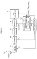
- FIG. 17 is a block diagram showing the configuration of a radio receiving apparatus according to another embodiment of the invention.
- FIG. 18 is a block diagram showing a radio receiving apparatus for UWB communications according to the prior art.
- FIG. 1 is a block diagram showing an example of the configuration of a radio receiving apparatus 1 according to an embodiment of the present invention.
- the radio receiving apparatus 1 shown in FIG. 1 is provided with an antenna 2 , a pulse demodulator 3 , an integrator 4 , an A/D converter 5 , a signal processor 6 , a reference clock generator 7 and a phase controller 8 .
- the antenna 2 receives a radio signal RF by UWB communications.
- the pulse demodulator 3 is a circuit for demodulating the radio signal RF received by the antenna 2 into pulses.
- the pulse demodulator 3 is provided with an amplifier 31 for amplifying the signal received by the antenna 2 , a filter 32 which is a bandpass filter for filtering the signal amplified by the amplifier 31 , and a detector 33 for outputting a detected signal S 1 obtained by performing envelope detection or peak detection to the integrator 4 , for example.
- the pulse demodulator 3 converts the signal received by the antenna 2 having a frequency band of 3.2 GHz, for example, into a frequency of about 500 Hz by detecting the received signal.
- the integrator 4 integrates the detected signal S 1 which has been frequency-converted by the pulse demodulator 3 and outputs an integral value thus obtained to the A/D converter 5 .
- the A/D converter 5 is an 8-bit (255-stage) A/D converter, for example, which converts the signal frequency-converted by the pulse demodulator 3 into a digital signal and outputs the same to the signal processor 6 as a signal level value AD.
- the signal processor 6 is configured with a central processing unit (CPU) for performing specified mathematical operations, a read-only memory (ROM) storing a specific control program, a random access memory (RAM) used for temporary data storage and/or as a regional level storage 61 , and peripheral circuits of these elements.
- CPU central processing unit
- ROM read-only memory
- RAM random access memory
- the signal processor 6 functions as a regional level acquirer 62 for acquiring the signal level value AD for each of plural regions into which the period of a pulse signal is divided and storing in the regional level storage 61 signal levels in the individual regions acquired therein under conditions where the signal level value AD is not received by the antenna 2 , a corrector 63 for correcting the signal levels in the individual regions received by the antenna 2 based on the signal levels stored in the regional level storage 61 for the individual regions, respectively, and a demodulator 64 for demodulating the radio signal RF according to the signal levels in the individual regions corrected by the corrector 63 and then outputting the demodulated radio signal as received data RD to the exterior by executing the control program stored in the ROM.
- a regional level acquirer 62 for acquiring the signal level value AD for each of plural regions into which the period of a pulse signal is divided and storing in the regional level storage 61 signal levels in the individual regions acquired therein under conditions where the signal level value AD is not received by the antenna 2 , a corrector 63
- the reference clock generator 7 Configured with a crystal oscillator, the reference clock generator 7 generates a clock signal having the same period as that of the pulse signal used for UWB communications and outputs the clock signal to the phase controller 8 .
- the phase controller 8 outputs a gate signal GT for controlling operating timing of the pulse demodulator 3 to the amplifier 31 and the integrator 4 based on the clock signal output from the reference clock generator 7 . More specifically, the phase controller 8 outputs a pulse signal having a pulselength approximately equal to or slightly longer than the pulselength of the pulse signal used for UWB communications, e.g., a pulse signal having a 10-ns pulselength, to the amplifier 31 and the integrator 4 at intervals of the pulse signal used for UWB communications, e.g., at intervals of 50 ns, as the gate signal GT indicating window periods.
- the phase controller 8 is configured to vary the timing of pulses of the gate signal GT indicating the window periods according to a control signal fed from the signal processor 6 .
- the amplifier 31 and the integrator 4 perform amplification and integration, respectively, in synchronism with the timing of the pulses of the gate signal GT, and not with other timing.
- the radio signal RF received by the antenna 2 is detected by the pulse demodulator 3 and integrated by the integrator 4 at the timing of the pulses of the gate signal GT, or during the window periods and, then, the integral value thus obtained is converted by the A/D converter 5 into the signal level value AD which is output to the signal processor 6 .
- FIG. 2 is a signal waveform chart for explaining the working of the radio receiving apparatus 1 shown in FIG. 1 .
- FIG. 2A shows an example of signal waveforms under ideal conditions where the radio receiving apparatus 1 is free of any influence of noise
- FIG. 2B shows an example of signal waveforms when periodic circuit noise is superimposed on a received signal.
- FIGS. 2A and 2B each show, from top to bottom, signal waveforms of the detected signal S 1 , the gate signal GT and an output signal of the integrator 4 .
- the radio signal RF received by the antenna 2 is demodulated into pulses by the pulse demodulator 3 and the demodulated pulses P 1 are output as the detected signal S 1 from the pulse demodulator 3 to the integrator 4 as shown in FIG. 2A . Then, the demodulated pulses P 1 are integrated by the integrator 4 and the result of integration is output to the A/D converter 5 at the timing of the pulses of the gate signal GT, or during each successive window period T 1 .
- the detected signal S 1 output from the pulse demodulator 3 contains the periodically superimposed noise in addition to the demodulated pulses P 1 , resulting in an increase in the level of an average value of noise, as shown in FIG. 2B .
- a peak value of the demodulated pulses P 1 is a value from the level of the average value of noise to a peak of the demodulated pulses P 1 , so that the peak value of the demodulated pulses P 1 decreases as a result of the increase in the level of the average value of noise.
- the regional level acquirer 62 first acquires the signal level value AD output from the A/D converter 5 , or the signal level value AD during each window period caused by the periodic noise produced by internal circuits, under conditions where the radio signal RF is not transmitted from an unillustrated UWB radio transmitting apparatus and thus the radio signal RF is not received by the antenna 2 .
- FIG. 3 is a signal waveform chart for explaining the working of the regional level acquirer 62 shown in FIG. 1 .
- FIG. 3 shows, from top to bottom, signal waveforms of the detected signal S 1 and the gate signal GT.
- the detected signal S 1 output from the pulse demodulator 3 does not contain the demodulated pulses P 1 and, therefore, the detected signal S 1 caused by the noise is output from the pulse demodulator 3 to the integrator 4 .
- the gate signal GT is output from the phase controller 8 to the amplifier 31 and the integrator 4 in phase with the window periods T 1 according to the control signal fed from the regional level acquirer 62 , the detected signal S 1 is integrated by the integrator 4 at the timing of the window periods T 1 , and the signal level value AD corresponding to the integral value thus obtained is output from the A/D converter 5 to the regional level acquirer 62 at first.
- the regional level acquirer 62 causes the phase controller 8 to output the gate signal GT in phase with the window periods T 1 for a specifically preset time period, e.g., for 8 ⁇ s.
- the regional level acquirer 62 averages the signal level values AD in the window periods T 1 obtained during 8 ⁇ s and causes the regional level storage 61 to store an average value thus obtained as an average level value AVT 1 in the window periods T 1 .
- the regional level acquirer 62 causes the phase controller 8 to output the gate signal GT with timing offset in phase from the window periods T 1 , e.g., in phase with window periods T 2 retarded by 1 ns from the window periods T 1 , for a specific time period, e.g., for 8 ⁇ s.
- the regional level acquirer 62 averages the signal level values AD in the window periods T 2 obtained over plural cycles during 8 ⁇ s and an average value thus obtained is stored in the regional level storage 61 as an average level value AVT 2 in the window periods T 2 .
- window periods T 1 -T 50 correspond to an example of plural regions mentioned in the claims.
- the regional level acquirer 62 may cause the regional level storage 61 to store the average level values AVT 1 -AVT 50 in the individual window periods with the individual window periods (regions) related to addresses of the regional level storage 61 , or with identification data indicating the individual window periods and the average level values AVT 1 -AVT 50 related to each other.
- the radio signal RF received by the antenna 2 is pulse-demodulated by the pulse demodulator 3 and integrated by the integrator 4 , and the result of integration is converted by the A/D converter 5 into the signal level values AD which are output to the corrector 63 .
- the corrector 63 corrects the signal level values AD by subtracting the average level values AVT 1 -AVT 50 stored in the regional level storage 61 , that is, the signal level values occurring during the individual window periods due to the periodic noise produced by the internal circuits, from the signal level values AD in the respective window periods T 1 -T 50 , and a corrected signal S 2 obtained by this correction is demodulated by the demodulator 64 and output as the received data RD to the exterior.
- the average level values AVT 1 -AVT 50 stored in the regional level storage 61 that is, the signal level values occurring during the individual window periods due to the periodic noise produced by the internal circuits, are corrected by the corrector 63 by subtracting the average level values AVT 1 -AVT 50 from the signal level values AD to decrease the influence of the noise having periodicity even when the noise having periodicity is superimposed on the signal level values AD output from the A/D converter 5 . It is therefore possible to improve reliability of communication.
- the regional level acquirer 62 is not limited to the aforementioned example in which the average level values AVT 1 -AVT 50 are stored in the regional level storage 61 but may be configured such that the regional level storage 61 directly stores the signal level values AD in the window periods T 1 -T 50 and the corrector 63 corrects the received signal by using the signal level values AD in the window periods T 1 -T 50 .
- the corrector 63 uses the average level values AVT 1 -AVT 50 , measurement accuracy of the signal level values in the individual window periods with the periodic noise produced by the internal circuits is improved, thereby enabling an improvement in the reliability of communication.
- the corrected signal S 2 is approximately equal to the reference value REF and thus becomes “240” under conditions where no radio signal RF is received as shown in FIG. 4 .
- the corrected signal S 2 takes a positive value even when the demodulated pulses P 1 take a negative value, for example, so that it becomes unnecessary to process negative values and, thus, signal processing is facilitated.
- the corrector 63 is required to perform mathematical operation of equation (3) for correcting the radio signal RF so that it becomes possible to relieve the work load required for mathematical operation during reception of the radio signal RF compared to a case where the mathematical operation of equation (1) is to be performed.
- the number of window periods may be determined as appropriate. The larger the number of window periods with the phase difference between successive window periods reduced, the more the accuracy of correction is improved, resulting in an improvement in the reliability of communication.
- this example may be modified such that the adjacent window periods exist next to one another without overlapping. This arrangement makes it possible to reduce the number of window periods defined in the pulse interval of the radio signal RF.
- each window period is set to 10 ns which is approximately equal to or slightly longer than the pulselength of the pulse signal used for UWB communications
- a time period of integrating noise components increases as a result of the lengthening of the window periods, resulting in a reduction in signal-to-noise ratio (S/N ratio), so that the window periods are to be properly set in light of a balance between an increase in circuit load caused by the increase in the number of window periods and the reduction in the S/N ratio caused by the lengthening of the window periods.
- the radio receiving apparatus 1 of the above-described embodiment may be configured to reduce the influence of noise to further improve the reliability of communication by use of a filter portion which can extract at least part of components in a frequency band used by the radio signal RF taking advantage of the fact that the pulse signal used for UWB communications is broadband.
- FIG. 5 is a block diagram showing the configuration of a radio receiving apparatus according to another embodiment of the present invention.
- this radio receiving apparatus 10 is configured with an antenna 2 , a pulse demodulator 11 , an integrator 4 , an A/D converter 5 , a signal processor 12 , a reference clock generator 7 , a phase controller 8 and a gain controller 13 .
- the radio receiving apparatus 10 shown in FIG. 5 differs from the radio receiving apparatus 1 shown in FIG. 1 in that the same is provided with the pulse demodulator 11 instead of the pulse demodulator 3 of the radio receiving apparatus 1 shown in FIG. 1 , the signal processor 12 instead of the signal processor 6 of the radio receiving apparatus 1 shown in FIG. 1 , and further the gain controller 104 .
- the former is otherwise the same as the latter.
- the pulse demodulator 11 is configured with an amplifier 31 , a filter portion 101 , an amplifier 102 and a detector 33 . Specifically, as compared to the pulse demodulator 3 shown in FIG. 1 , the pulse demodulator 11 differs from the radio receiving apparatus 1 shown in FIG. 1 in that the same is provided with the filter portion 101 instead of the filter 32 of the pulse demodulator 3 shown in FIG. 1 and further the amplifier 102 connected between the filter portion 101 and the detector 33 . The former is otherwise the same as the latter.
- the signal processor 12 is configured with a regional level storage 61 , a regional level acquirer 62 , a corrector 63 and a demodulator 121 . Specifically, as compared to the signal processor 6 shown in FIG. 1 , the signal processor 12 differs from the radio receiving apparatus 1 shown in FIG. 1 in that the same is provided with the demodulator 121 instead of the demodulator 64 shown in FIG. 1 . The former is otherwise the same as the latter.
- FIG. 6 is a waveform chart of a radio signal used for UWB communications.
- FIG. 6A shows the radio signal
- FIG. 6B shows pulses of the radio signal.
- FIG. 7 is a waveform chart for explaining receive timing of the radio signal used for UWB communications.
- FIG. 7A shows an output of a radio transmitting apparatus (the pulses of the radio signal)
- FIG. 7B shows an output of the detector
- FIG. 7C shows an integration control signal Tint.
- FIG. 8 is a waveform chart for explaining a method of demodulating the radio signal used for UWB communications.
- FIG. 8A shows the radio signal (transmitted signal)
- FIG. 8B shows values AD A/D-converted by the A/D converter 5
- FIG. 8C shows a demodulated signal.
- the radio signal RF transmitted from the unillustrated radio transmitting apparatus is a pulsating signal made up of a synchronizing pulse train used by the radio receiving apparatus 10 to accomplish synchronization with pulses of the pulse signal and a pulse train corresponding to data to be transmitted (baseband signal).
- the synchronizing pulse train is a signal in which pulses for UWB communications are repeated at specific intervals Trep as shown in FIG. 6B .
- the number of repeated pulses is set in such a way that pulse positions can be detected on the side of the radio receiving apparatus 10 .
- the synchronizing pulse train is configured with the addition of the existence or non-existence of the pulse train at the end of the synchronizing pulse train indicating the end of pulse synchronization.
- the transmitted data is constructed such that the UWB communications pulses are repeated N times at the aforementioned intervals Trep when the data value is “1”, and time during which nothing is output lasts for a time period TD equal to Trep ⁇ N when the data value is “0”.
- This time period TD is a 1-bit period of the aforementioned data to be transmitted (baseband signal).
- the data to be transmitted is represented by on/off keying in the aforementioned example, the same may be expressed by other form of modulation, such as bi-phase modulation.
- the radio signal RF transmitted from the aforementioned radio transmitting apparatus is received by the broadband antenna 2 , components in the frequency band used by the radio signal RF are extracted by the filter portion 101 and subjected to envelope detection or peak detection in the detector 33 and, then, the result of detection is input into the integrator 4 .
- the integrator 4 responds to the integration control signal Tint output from the demodulator 121 of the signal processor 12 for controlling the timing of integration periods in the aforementioned intervals Trep, the integrator 4 performs operation for accumulating detected outputs of the detector 33 N times according to the integration control signal Tint when the integration control signal Tint is active at high level.
- An accumulated value thus obtained is A/D-converted by the A/D converter 5 and the A/D-converted value is compared with a specifically preset threshold by a pulse judgment portion 121 a of the demodulator 121 , whereby the A/D-converted value is judged as “1” or “0” data mentioned above.
- the pulse judgment portion 121 a of the demodulator 121 further demodulates the “1” or “0” data obtained as mentioned above to extract the aforementioned baseband signal therefrom and controls timing of the aforementioned integration periods in such a way that the synchronizing pulse train will be detected during a period when the aforementioned synchronizing pulse train is not detected.
- the UWB communications pulses transmitted from the aforementioned radio transmitting apparatus are approximately 2- to 3-ns pulses, for example, recurring at the aforementioned intervals Trep as shown in FIG. 7A .
- the demodulator 121 controls the integration periods of the integrator 4 according to aforementioned integration control signal Tint so that the integrator 4 determines the accumulated value by accumulating the detected outputs of the detector 33 N times as shown in FIG. 7B at successive points of the phases ⁇ 1 - ⁇ m throughout the aforementioned time period TD.
- the A/D-converted value of the accumulated value is equal to or larger than the specific threshold TH as shown in FIG.
- the demodulator 121 judges the accumulated value as the aforementioned “1” data, and when the A/D-converted value of the accumulated value is smaller than the specific threshold TH, the demodulator 121 judges the accumulated value as the aforementioned “0” data, whereby the demodulator 121 obtains the demodulated signal as shown in FIG. 8C corresponding to the radio signal RF (transmitted signal) as shown in FIG. 8A .
- the pulse judgment portion 121 a detects a time slot (phase point of ⁇ 3 in the example shown in FIG. 7 ) corresponding to the own apparatus during a search for a synchronization timing carried out by accumulating the detected outputs of the detector 33 while offsetting the aforementioned time slot in steps of the time period Ton during the synchronizing pulse train, a later portion of the search is canceled.
- the pulse judgment portion 121 a carries out the search up to the phase point of ⁇ 4 and judges this phase point as the synchronization timing as the A/D-converted value obtained at a phase point of ⁇ 3 is larger.
- the aforementioned filter portion 101 is configured to be able to extract at least part of the components in the frequency band used by the radio signal RF and the radio receiving apparatus 10 is provided with the aforementioned gain controller 13 .
- FIG. 9 is a block diagram showing an example of the configuration of the filter portion
- FIG. 10 is a graph showing an example of filter passband characteristics for the radio signal used for UWB communications.
- FIG. 10A shows frequency characteristics of transmitted power of the radio signal used for UWB communications, the horizontal axis representing frequency and the vertical axis representing power.
- FIG. 10B shows the filter passband characteristics, the horizontal axis representing frequency.
- the filter portion 101 is configured with two filters 101 a , 101 b and switching devices 101 c , 101 d disposed parallel to each other on upstream and downstream sides of the filters 101 a , 101 b , respectively, for switching a signal path to one of the filters 101 a , 101 b .
- the switching devices 101 c , 101 d are controlled to alternately switch the signal path in an interlocked fashion by a filter switching signal SEL fed from the gain controller 13 .
- the transmitted signal (radio signal RF) from the aforementioned radio transmitting apparatus is an impulse signal having a broad bandwidth of 3-5 GHz as shown in FIG. 10A , for example.
- the characteristics of the aforementioned filters 101 a , 101 b are such that the filter 101 a allows components on a low-frequency side to pass through and the filter 101 b allows components on a high-frequency side to pass through as shown in FIG. 10B , for example.
- the filter portion 101 may also be configured such that the filter 101 a allows components in an entire band shown in FIG. 10A to pass through and the filter 101 b allows components on the low-frequency side or high-frequency side where an interfering wave is less likely to occur to pass through, for example. Furthermore, the filter portion 101 may be configured such that there are provided three filters including filters for passing the components on the low-frequency side and the high-frequency side in addition to a filter for passing the components in the entire band and these filters can be switched. In other words, the filter portion 101 should be configured to be able to extract components in at least part of the frequency band used by the radio signal RF. Moreover, the filter portion 101 may be configured such that the aforementioned filters 101 a , 101 b are disposed in series with each other and the aforementioned switching devices 101 c , 101 d bypass these filters 101 a , 101 b , respectively.
- the gain controller 13 responding to a pulse sensing signal SEN input from the pulse judgment portion 121 a indicating whether the pulse judgment portion 121 a is synchronized with received pulses, the gain controller 13 first determines a variance of the values A/D-converted by the A/D converter 5 during a period when no pulses are detected. The gain controller 13 then adjusts a frequency passband of the filter portion 101 by outputting the filter switching signal SEL according to the variance obtained by the gain controller 13 .
- FIGS. 11-15 are diagrams for explaining the aforementioned adjustment operation.
- FIG. 13A shows a relation between a frequency spectrum of the transmitted signal and a frequency spectrum of the interfering wave, the horizontal axis representing frequency and the vertical axis representing power.
- FIG. 13B shows frequency characteristics of the filters, the horizontal axis representing frequency.
- FIGS. 14A and 15A show transmitted signals
- FIGS. 14B and 15B show received signals
- FIGS. 14C and 15C show A/D-converted values
- FIGS. 14D and 15D show demodulated signals.
- an interfering wave source 202 generates an interfering wave (noise) which becomes a CW wave in the filter 101 a and contaminates the transmitted signal (radio signal RF) from a transmitting antenna 201 of the aforementioned radio transmitting apparatus as shown in FIG. 11 , for example.
- Signal waveforms of the transmitted signal and the interfering wave that reach the receiving antenna 2 in this case are as shown in FIG. 12A and their frequency spectra are as shown in FIG. 13A , from top to bottom, respectively.
- the interfering wave is attenuated in the high-frequency side filter 101 b as shown in FIG. 12C , so that it is possible to extract only the transmitted signal when the there is a relationship expressed by (transmitted signal)>>(interfering wave) in this frequency band in terms of the field strength.
- the signal output from the amplifier 102 after passing through the filter 101 b of the filter portion 101 when the transmitted signal shown in FIG. 15A is input becomes as shown in FIG. 15B . For this reason, when the signal shown in FIG.
- the pulse judgment portion 121 a of the demodulator 121 can accomplish synchronization and obtain a demodulated signal corresponding to the transmitted signal from a succeedingly transmitted data train as shown in FIG. 15D .
- the gain controller 13 may be configured to regularly select the filters 101 a , 101 b at alternate intervals of specific time periods and search through conditions of interfering waves in individual frequency bands to receive the signal by switching to one of the frequency bands containing less interfering waves. Alternatively, the gain controller 13 may be configured such that the same is switched to one filter when it becomes impossible to accomplish synchronization with the currently selected other filter.
- the radio receiving apparatus 10 thus configured can demodulate the broadband radio signal to extract baseband components of the transmitted signal from components of a frequency band unburied in the interfering wave even when the level of the interfering wave is high and the transmitted signal is buried therein.
- it is possible to enhance interfering wave withstand capability of the radio receiving apparatus 10 without causing a reduction in receiving sensitivity by avoiding a frequency region in which any interfering wave occurs when the interfering wave is present in the frequency band used by the radio signal RF. For this reason, the influence of noise is reduced, making it possible to further improve the reliability of communication.
- the amplifier 102 may be a variable-gain amplifier, in which gain of the amplifier 102 is adjusted by an amplification factor switching signal CTL fed from the gain controller 13 .
- the gain controller 13 selects one of the filters 101 a , 101 b which makes the power of the interfering wave lower, or the variance smaller, when the two filters 101 a , 101 b are switched as mentioned above and it is judged that the variance, or the amount of variations, of the values A/D-converted in each case is equal to or larger than a specified level and the interfering wave exists in both cases and, in addition, the gain controller 13 switches the gain of the amplifier 102 to a smaller value as the variance becomes larger according to the amplification factor switching signal CTL.
- a variance of the A/D-converted values obtained in a unit time W 1 when there is no signal received by the antenna 2 is given in advance as an initial value. If an interfering wave occurs in this condition, the aforementioned variance increases according to the power level of the interfering wave as shown in a time W 2 in FIG. 16 . However, since the amplification factor of the amplifier 102 is decreased according to an increase in the variance upon switching to one of the filters 101 a , 101 b which passes lower power of the interfering wave (or to the frequency side which gives a better sensitivity) as mentioned above, the demodulator 121 sets the variance of the A/D-converted values to the initially set value shown in the time W 1 .
- the radio receiving apparatus 10 can keep the level of reduction in the aforementioned receiving sensitivity to a minimum level corresponding to the power of the aforementioned interfering wave.
- the gain controller 13 determines the aforementioned variance during the period when no pulses are detected responding to the pulse sensing signal SEN fed from the pulse judgment portion 121 a as mentioned earlier, it is possible to eliminate variations in the variance caused by variations in the A/D-converted value at the occurrence of transmitted pulses ( ⁇ 3 regions in FIG. 8 ) and to exactly determine the variance of noise components, such as thermal noise and interfering waves, occurring during a period when the received signal is absent. As a result, it is possible to properly adjust the frequency passband of the filter portion 101 and the gain of the amplifier 102 .
- FIG. 17 is a block diagram showing the configuration of a radio receiving apparatus according to another embodiment of the present invention.
- the radio receiving apparatus 10 may be configured as a radio receiving apparatus 10 A which receives a pulsating radio signal having a specific period with timing synchronized with this period and demodulates the received signal to extract a baseband signal from a pulse train of the radio signal, the radio receiving apparatus 10 A comprising a filter portion 101 which can extract at least part of components in a frequency band used by the aforementioned radio signal with the received signal input into the filter portion 101 , a detector 33 for detecting an envelope or peaks of an output of the aforementioned filter portion 101 , an integrator 4 for accumulating an output of the aforementioned detector 33 for a specific integration period, an A/D converter 5 for A/D-converting an output voltage of the aforementioned integrator 4 , a demodulator 121 for adjusting the integration period of the aforementioned detector 33 based on values A/D-converted by the aforementioned A
- the radio receiving apparatus 10 A may be configured to be further provided with an amplifier 102 connected between the filter portion 101 and the detector 33 , so that gain of the amplifier 102 is adjusted by a signal fed from the gain controller 13 .
- the radio receiving apparatus 10 A thus configured can provide an enhanced interfering wave withstand capability without causing a reduction in receiving sensitivity by avoiding a frequency region in which any interfering wave occurs.
- a radio receiving apparatus for receiving a radio signal having pulsating signals occurring at specific periods, the radio receiving apparatus comprising a receiver portion for receiving the aforementioned radio signal, a regional level acquirer for acquiring a signal level obtained by the aforementioned receiver portion in each of plural regions into which each of the aforementioned periods is divided, a regional level storage for storing signal levels acquired by the aforementioned regional level acquirer in the aforementioned individual regions under conditions where the aforementioned radio signal is not received by the aforementioned receiver portion for the aforementioned individual regions, a corrector portion for correcting the signal levels in the aforementioned individual regions received by the aforementioned receiver portion based on the signal levels in the aforementioned individual regions stored in the aforementioned regional level storage, respectively, and a demodulator portion for demodulating the aforementioned radio signal according to the signal levels in the individual regions corrected by the aforementioned corrector portion.
- the radio signal having the pulsating signals occurring at the specific periods is received by the receiver portion and the signal levels of the radio signal obtained by the receiver portion are acquired individually for the plural regions into which each of pulse periods is divided. Then, the signal levels acquired in the individual regions under conditions where the radio signal is not received are stored in the regional level storage for the individual regions. Further, the signal levels in the individual regions received by the receiver portion are corrected based on the signal levels in the individual regions stored in the regional level storage, respectively, and the radio signal is demodulated according to the corrected signal levels in the individual regions. Thus, the influence of noise having periodicity is decreased by this correction, making it possible to improve reliability of communication.
- a radio receiving apparatus is the radio receiving apparatus according to the aforementioned first mode, wherein the aforementioned regional level acquirer acquires the aforementioned signal levels in the aforementioned plural regions while successively offsetting the regions in which the aforementioned signal levels are acquired.
- the invention provides a radio receiving apparatus which decreases the influence of noise having periodicity and improves reliability of communication with the provision of the regional level acquirer which acquires the signal levels in the plural regions while successively offsetting the regions in which the aforementioned signal levels are acquired.
- a radio receiving apparatus is the radio receiving apparatus according to the aforementioned first or second mode, wherein the aforementioned regional level acquirer acquires the signal levels in the aforementioned individual regions over the aforementioned plural periods, calculates average values of the signal levels thus acquired in time durations corresponding to the aforementioned individual regions in each of the aforementioned plural periods, and causes the aforementioned regional level storage to store the average values calculated for the individual time durations as the signal levels in the aforementioned individual regions.
- the average values in the individual time durations are regarded as the signal levels in the individual regions so that measurement accuracy of signal level values in individual window periods with periodic noise produced by internal circuits is improved.
- the reliability of communication is therefore improved.
- a radio receiving apparatus is the radio receiving apparatus according to one of the aforementioned first to third modes, wherein the aforementioned corrector portion performs the aforementioned correction by subtracting the signal levels in the aforementioned individual regions stored in the aforementioned regional level storage from the signal levels in the aforementioned individual regions received by the aforementioned receiver portion, respectively.
- the invention provides a radio receiving apparatus which decreases the influence of noise having periodicity and improves reliability of communication with the provision of the corrector portion which performs the correction by subtracting the signal levels in the individual regions stored in the regional level storage from the signal levels in the individual regions received by the receiver portion, respectively.
- a radio receiving apparatus is the radio receiving apparatus according to one of the aforementioned first to third modes, wherein the aforementioned corrector portion performs the aforementioned correction by adding differences between a preset reference value and the signal levels in the aforementioned individual regions stored in the aforementioned regional level storage to the signal levels in the aforementioned individual regions received by the aforementioned receiver portion, respectively.
- the signal corrected under conditions where no radio signal is received becomes approximately equal to the reference value. Therefore, the corrected signal takes a positive value even when demodulated pulses take a negative value, for example, so that it becomes unnecessary to process negative values and, thus, signal processing is facilitated.
- a radio receiving apparatus is the radio receiving apparatus according to the aforementioned first mode, wherein the aforementioned regional level acquirer causes the aforementioned regional level storage to store differences between a preset reference value and the signal levels acquired in the aforementioned individual regions as signal levels in the aforementioned individual regions, and the aforementioned corrector portion performs the aforementioned correction by adding the signal levels in the aforementioned individual regions stored in the aforementioned regional level storage to the signal levels in the aforementioned individual regions received by the aforementioned receiver portion, respectively.
- the regional level acquirer causes the regional level storage to store the differences between the preset reference value and the signal levels acquired in the individual regions as the signal levels in the individual regions, so that it becomes possible to relieve the work load required for mathematical operation during reception of the radio signal.
- a radio receiving apparatus is the radio receiving apparatus according to one of the aforementioned first to sixth modes, wherein the aforementioned receiver portion is provided with an antenna portion for receiving the aforementioned radio signal and outputting the received signal, a filter portion which can extract at least part of components in a frequency band used by the aforementioned radio signal with the received signal input into the filter portion, a detector portion for detecting one of an envelope and peaks of an output of the aforementioned filter portion, an integrator portion for accumulating an output of the aforementioned detector portion for a specific integration period, and an analog-to-digital converter for A/D-converting an output voltage of the aforementioned integrator portion, wherein the aforementioned demodulator portion adjusts the aforementioned integration period of the aforementioned integrator portion based on values A/D-converted by the aforementioned analog-to-digital converter, and the radio receiving apparatus further comprises a gain controller for adjusting for adjusting a frequency passband of the aforementioned filter portion according to a variance of the values A
- the components in the frequency band used by the radio signal are extracted from signal components received by a broadband antenna, for example, by the filter portion, and the envelope or peaks of the extracted components are detected by the detector portion. Then, the output of the detector portion is accumulated for the specific integration period by the integrator portion and the result of accumulation is A/D-converted by the analog-to-digital converter.
- a comparison between the values A/D-converted by the analog-to-digital converter and a specific threshold made by the demodulator portion makes it possible to judge the A/D-converted values as “1” or “0” data.
- the demodulator portion demodulates the “1” or “0” data obtained to extract a baseband signal therefrom and controls timing of the aforementioned integration period in such a way that a synchronizing pulse train will be detected when the synchronizing pulse train has not been detected.
- the filter portion is configured to have a capability to extract at least part of the components in the frequency band used by the radio signal and the radio receiving apparatus is provided with the gain controller which adjusts the frequency passband of the filter portion according to the variance of the values A/D-converted by the analog-to-digital converter.
- the filter portion is configured to include a filter which passes components on a low-frequency side of the frequency passband used by the radio signal and a filter which passes components on a high-frequency side
- the filter portion is switched to the filter which passes the high-frequency side components when the filter which passes the low-frequency side components is currently selected and pulses are detected at other than a correct synchronization timing as a result of an increase in the variance, or the amount of variations, of the A/D-converted values caused by an interfering wave.
- the filter portion is configured to include a filter which passes components in the entire passband and a filter which passes components on the low-frequency side or high-frequency side
- the filter portion is switched to the filter which passes the high-frequency side or high-frequency side components when the filter which passes the entire passband is currently selected and pulses are detected at other than a correct synchronization timing as a result of an increase in the variance of the A/D-converted values caused by an interfering wave, for example.
- a radio receiving apparatus is the radio receiving apparatus according to the aforementioned seventh mode, wherein the aforementioned receiver portion is further provided with an amplifier portion connected between the aforementioned filter portion and the detector portion, wherein gain of the aforementioned amplifier portion is adjusted by a signal fed from the aforementioned gain controller.
- the gain of the amplifier portion is reduced preferably after the frequency passband of the filter portion has been adjusted, and the radio receiving apparatus is controlled such that the variance of the A/D-converted values becomes approximately constant when the variance increases due to an interfering wave.
- the receiving sensitivity lowers as a consequence, it is possible to demodulate a received signal having a higher level than the interfering wave when such a signal is input. Therefore, the radio receiving apparatus can receive the radio signal if the received signal has power greater than power of the interfering wave even when the interfering wave is unavoidable.
- a radio receiving apparatus is the radio receiving apparatus according to the aforementioned seventh or eighth mode, wherein the aforementioned gain controller judges whether any received signal exists from the variance of the values A/D-converted by the aforementioned analog-to-digital converter and restricts acquisition of the variance during the integration period in which the received signal exists.
- the gain controller judges whether any received signal exists from the variance and restricts acquisition of the variance during the integration period in which the received signal exists.
- a radio receiving method for receiving a radio signal having pulsating signals occurring at specific periods, the radio receiving method comprising a step of receiving the aforementioned radio signal by a receiver portion, a step of acquiring a signal level obtained by the aforementioned receiver portion in each of plural regions into which each of the aforementioned periods is divided, a step of storing signal levels acquired in the aforementioned individual regions under conditions where the radio signal is not received by the aforementioned receiver portion in a regional level storage for the aforementioned individual regions, a step of correcting the aforementioned received signal levels in the aforementioned individual regions based on the signal levels in the aforementioned individual regions stored in the aforementioned regional level storage, respectively, and a step of demodulating the aforementioned radio signal according to the aforementioned corrected signal levels in the individual regions.
- the radio signal having the pulsating signals occurring at the specific periods is received by the receiver portion and the signal levels of the radio signal obtained by the receiver portion are acquired individually for the plural regions into which each of pulse periods is divided. Then, the signal levels acquired in the individual regions under conditions where the radio signal is not received are stored in the regional level storage for the individual regions. Further, the signal levels in the individual regions received by the receiver portion are corrected based on the signal levels in the individual regions stored in the regional level storage, respectively, and the radio signal is demodulated according to the corrected signal levels in the individual regions. Thus, the influence of noise having periodicity is decreased by this correction, making it possible to improve reliability of communication.
- the present invention which relates to a radio receiving apparatus and a radio receiving method for receiving an ultra-wideband communications radio signal, can provide a radio receiving apparatus and a radio receiving method which make it possible to improve reliability of communication.
Abstract
Description
- Patent Document 1: Japanese Unexamined Patent Publication No. 2005-217899
- Patent Document 2: Japanese Unexamined Patent Publication No. 1998-508725
- Patent Document 3: Japanese Unexamined Patent Publication No. 2006-94169
S2=ADn+(REF−AVTn) (1)
-
- (where n=1, 2, 3 . . . , 50)
Cn=REF−AVTn (2)
-
- (where n=1, 2, 3 . . . , 50)
S2=ADn+Cn (3)
-
- (where n=1, 2, 3 . . . , 50)
Claims (10)
Applications Claiming Priority (3)
| Application Number | Priority Date | Filing Date | Title |
|---|---|---|---|
| JP2005-278271 | 2005-09-26 | ||
| JP2005278271A JP2007089053A (en) | 2005-09-26 | 2005-09-26 | Radio reception apparatus and radio reception method |
| PCT/JP2006/319013 WO2007034956A1 (en) | 2005-09-26 | 2006-09-26 | Radio receiving apparatus and radio receiving method |
Publications (2)
| Publication Number | Publication Date |
|---|---|
| US20090154526A1 US20090154526A1 (en) | 2009-06-18 |
| US7940863B2 true US7940863B2 (en) | 2011-05-10 |
Family
ID=37888997
Family Applications (1)
| Application Number | Title | Priority Date | Filing Date |
|---|---|---|---|
| US12/066,390 Expired - Fee Related US7940863B2 (en) | 2005-09-26 | 2006-09-26 | Radio receiving apparatus and radio receiving method |
Country Status (5)
| Country | Link |
|---|---|
| US (1) | US7940863B2 (en) |
| EP (1) | EP1940036B1 (en) |
| JP (1) | JP2007089053A (en) |
| KR (1) | KR100965680B1 (en) |
| WO (1) | WO2007034956A1 (en) |
Families Citing this family (7)
| Publication number | Priority date | Publication date | Assignee | Title |
|---|---|---|---|---|
| CN102047576B (en) * | 2008-05-27 | 2014-07-30 | 松下电器产业株式会社 | Reception device |
| US20100067364A1 (en) * | 2008-09-12 | 2010-03-18 | Francis Swarts | Method and system for variance-based automatic gain control in ofdm systems |
| US20110159817A1 (en) * | 2009-12-29 | 2011-06-30 | Pirelli Tyre S.P.A. | Method and system for managing communications between sensor devices included in a tyre and a sensor coordinator device |
| EP2429089A1 (en) * | 2010-09-08 | 2012-03-14 | Fraunhofer-Gesellschaft zur Förderung der Angewandten Forschung e.V. | Receiver and method for determining a time measure depending on a time of arrival of a pulse signal |
| JP6241642B2 (en) * | 2013-05-10 | 2017-12-06 | 国立研究開発法人情報通信研究機構 | Wireless detector and wireless detection method |
| WO2016086065A1 (en) * | 2014-11-25 | 2016-06-02 | Maxim Integrated Products, Inc. | Peak detection in data stream |
| KR102071224B1 (en) * | 2019-02-19 | 2020-01-30 | 한화시스템 주식회사 | Radiometer |
Citations (16)
| Publication number | Priority date | Publication date | Assignee | Title |
|---|---|---|---|---|
| JPH0233214A (en) | 1988-07-22 | 1990-02-02 | Matsushita Electric Ind Co Ltd | Digital filter for decimation |
| WO1996009694A1 (en) | 1994-09-20 | 1996-03-28 | Time Domain Systems, Inc. | An ultrawide-band communications system and method |
| JP2998794B2 (en) | 1997-01-28 | 2000-01-11 | 日本電気株式会社 | Periodic noise removing apparatus and periodic noise removing method |
| JP2003101509A (en) | 2001-09-21 | 2003-04-04 | Sony Corp | Radio transmission method by ultrawide band communication, and its transmission device and reception device |
| US20040029610A1 (en) | 2002-06-10 | 2004-02-12 | Matsushita Electric Works, Ltd. | Portable radio communication terminal and call center apparatus |
| US6785392B1 (en) * | 2000-04-25 | 2004-08-31 | Tripath Technology, Inc. | Methods and apparatus for enabling or disabling an amplifier |
| US6834073B1 (en) * | 2000-05-26 | 2004-12-21 | Freescale Semiconductor, Inc. | System and method for baseband removal of narrowband interference in ultra wideband signals |
| EP1503513A1 (en) | 2003-07-30 | 2005-02-02 | Mitsubishi Electric Information Technology Centre Europe B.V. | Method for identifying the beginning of a UWB pulse sequence |
| US20050037805A1 (en) | 2003-08-12 | 2005-02-17 | Samsung Electronics Co., Ltd. | Signal reception apparatus and method for multi-band utlra-wideband communication systems |
| KR20050061928A (en) | 2003-12-19 | 2005-06-23 | 한국전자통신연구원 | Auto gain control apparatus |
| JP2005197918A (en) | 2004-01-06 | 2005-07-21 | Matsushita Electric Ind Co Ltd | Receiver of cordless telephone set |
| JP2005217899A (en) | 2004-01-30 | 2005-08-11 | Handotai Rikougaku Kenkyu Center:Kk | Uwb receiving circuit |
| JP2006060737A (en) | 2004-08-24 | 2006-03-02 | Matsushita Electric Works Ltd | Communication method, pulse synchronization circuit and receiver |
| JP2006094169A (en) | 2004-09-24 | 2006-04-06 | Matsushita Electric Works Ltd | Receiver |
| US7110473B2 (en) * | 1998-12-11 | 2006-09-19 | Freescale Semiconductor, Inc. | Mode controller for signal acquisition and tracking in an ultra wideband communication system |
| US7200361B2 (en) * | 2003-10-03 | 2007-04-03 | Kabushiki Kaisha Toshiba | Wireless communication apparatus, wireless communication method and wireless communication media |
-
2005
- 2005-09-26 JP JP2005278271A patent/JP2007089053A/en active Pending
-
2006
- 2006-09-26 WO PCT/JP2006/319013 patent/WO2007034956A1/en active Application Filing
- 2006-09-26 EP EP20060810538 patent/EP1940036B1/en not_active Not-in-force
- 2006-09-26 US US12/066,390 patent/US7940863B2/en not_active Expired - Fee Related
- 2006-09-26 KR KR20087008190A patent/KR100965680B1/en not_active IP Right Cessation
Patent Citations (28)
| Publication number | Priority date | Publication date | Assignee | Title |
|---|---|---|---|---|
| JPH0233214A (en) | 1988-07-22 | 1990-02-02 | Matsushita Electric Ind Co Ltd | Digital filter for decimation |
| US5995534A (en) | 1994-09-20 | 1999-11-30 | Time Domain Corporation | Ultrawide-band communication system and method |
| US5677927A (en) | 1994-09-20 | 1997-10-14 | Pulson Communications Corporation | Ultrawide-band communication system and method |
| JPH10508725A (en) | 1994-09-20 | 1998-08-25 | タイム ドメイン コーポレイション | Ultra wideband communication system and method |
| US5960031A (en) | 1994-09-20 | 1999-09-28 | Time Domain Corporation | Ultrawide-band communication system and method |
| US5963581A (en) | 1994-09-20 | 1999-10-05 | Time Domain Corporation | Ultrawide-band communication system and method |
| WO1996009694A1 (en) | 1994-09-20 | 1996-03-28 | Time Domain Systems, Inc. | An ultrawide-band communications system and method |
| US6031862A (en) | 1994-09-20 | 2000-02-29 | Time Domain Corporation | Ultrawide-band communication system and method |
| JP2998794B2 (en) | 1997-01-28 | 2000-01-11 | 日本電気株式会社 | Periodic noise removing apparatus and periodic noise removing method |
| US7110473B2 (en) * | 1998-12-11 | 2006-09-19 | Freescale Semiconductor, Inc. | Mode controller for signal acquisition and tracking in an ultra wideband communication system |
| US6785392B1 (en) * | 2000-04-25 | 2004-08-31 | Tripath Technology, Inc. | Methods and apparatus for enabling or disabling an amplifier |
| US6834073B1 (en) * | 2000-05-26 | 2004-12-21 | Freescale Semiconductor, Inc. | System and method for baseband removal of narrowband interference in ultra wideband signals |
| JP2003101509A (en) | 2001-09-21 | 2003-04-04 | Sony Corp | Radio transmission method by ultrawide band communication, and its transmission device and reception device |
| US20040029610A1 (en) | 2002-06-10 | 2004-02-12 | Matsushita Electric Works, Ltd. | Portable radio communication terminal and call center apparatus |
| US20050031043A1 (en) | 2003-07-30 | 2005-02-10 | Mitsubishi Denki Kabushiki Kaisha | Method for identifying the beginning of a UWB pulse sequence |
| EP1503513A1 (en) | 2003-07-30 | 2005-02-02 | Mitsubishi Electric Information Technology Centre Europe B.V. | Method for identifying the beginning of a UWB pulse sequence |
| KR20050019943A (en) | 2003-08-12 | 2005-03-04 | 삼성전자주식회사 | Receiving apparatus for muti-band UWB communication system and method of using the same |
| US7369829B2 (en) | 2003-08-12 | 2008-05-06 | Samsung Electronics Co., Ltd. | Signal reception apparatus and method for multi-band ultra-wideband communication systems |
| US20050037805A1 (en) | 2003-08-12 | 2005-02-17 | Samsung Electronics Co., Ltd. | Signal reception apparatus and method for multi-band utlra-wideband communication systems |
| US7200361B2 (en) * | 2003-10-03 | 2007-04-03 | Kabushiki Kaisha Toshiba | Wireless communication apparatus, wireless communication method and wireless communication media |
| US20050135513A1 (en) | 2003-12-19 | 2005-06-23 | Kang Hun S. | Automatic gain control apparatus |
| KR20050061928A (en) | 2003-12-19 | 2005-06-23 | 한국전자통신연구원 | Auto gain control apparatus |
| US7436913B2 (en) | 2003-12-19 | 2008-10-14 | Electronics And Telecommunications Research Institute | Automatic gain control apparatus |
| JP2005197918A (en) | 2004-01-06 | 2005-07-21 | Matsushita Electric Ind Co Ltd | Receiver of cordless telephone set |
| US20050213635A1 (en) | 2004-01-30 | 2005-09-29 | Semiconductor Technology Academic Research Center | Ultra-wideband receiver |
| JP2005217899A (en) | 2004-01-30 | 2005-08-11 | Handotai Rikougaku Kenkyu Center:Kk | Uwb receiving circuit |
| JP2006060737A (en) | 2004-08-24 | 2006-03-02 | Matsushita Electric Works Ltd | Communication method, pulse synchronization circuit and receiver |
| JP2006094169A (en) | 2004-09-24 | 2006-04-06 | Matsushita Electric Works Ltd | Receiver |
Non-Patent Citations (9)
| Title |
|---|
| English language Abstract of JP 10-508725, Aug. 25, 1998. |
| English language Abstract of JP 2003-101509, Apr. 4, 2003. |
| English language Abstract of JP 2005-217899, Aug. 11, 2005. |
| English language Abstract of JP 2006-94169, Mar. 28, 1996. |
| English language Abstract of JP 2-033214 A, Feb. 2, 1990. |
| English language Abstract of JP 2998794 B2, Nov. 5, 1999. |
| English language Abstract of KR 2005-0019943, Mar. 4, 2005. |
| English language Abstract of KR 2005-0061928, Jun. 23, 2005. |
| Japan Office action issued in corresponding JP 2006-171526, dated Dec. 7, 2010, along with a partial English language translation thereof. |
Also Published As
| Publication number | Publication date |
|---|---|
| EP1940036A1 (en) | 2008-07-02 |
| EP1940036B1 (en) | 2012-02-22 |
| US20090154526A1 (en) | 2009-06-18 |
| KR20080065608A (en) | 2008-07-14 |
| EP1940036A4 (en) | 2010-10-13 |
| KR100965680B1 (en) | 2010-06-24 |
| WO2007034956A1 (en) | 2007-03-29 |
| JP2007089053A (en) | 2007-04-05 |
Similar Documents
| Publication | Publication Date | Title |
|---|---|---|
| US7940863B2 (en) | Radio receiving apparatus and radio receiving method | |
| US20110069738A1 (en) | Reception device | |
| US10805884B2 (en) | Power-save system for detection of bluetooth long range packets | |
| KR101188834B1 (en) | Wireless receiver | |
| US20060120441A1 (en) | Receiver | |
| JP2000151318A (en) | Peripheral level detecting device for radio portable terminal | |
| US8089950B2 (en) | Wireless communication equipment and wireless communication method | |
| CN108234042B (en) | Digital signal detection method, device, computer equipment and readable storage medium | |
| US20230032217A1 (en) | Preamble Signal for Wakeup Communication in a Wireless Communication System | |
| JP4822366B2 (en) | Two-way wireless communication device | |
| JP5564282B2 (en) | Receiver circuit and receiver | |
| US7957454B2 (en) | Transmitter, receiver, and data communications system and method | |
| JP3643088B2 (en) | Data slicer | |
| JP2007036593A (en) | Radio receiver and radio-receiving method | |
| JP2005210170A (en) | Frequency-hopping wireless communication apparatus and carrier sense apparatus | |
| JP4994865B2 (en) | Wireless receiver | |
| JP5563922B2 (en) | Wireless communication device | |
| JP4710733B2 (en) | Wireless receiver | |
| JP2003008474A (en) | Spread spectrum communication unit | |
| US20230261690A1 (en) | Dual Chirp Modulation Scheme | |
| JP4877078B2 (en) | Wireless receiver | |
| EP1026836A1 (en) | Method and apparatus for detecting a constant frequency part of a telecommunication signal |
Legal Events
| Date | Code | Title | Description |
|---|---|---|---|
| AS | Assignment |
Owner name: MATSUSHITA ELECTRIC WORKS, LTD., JAPAN Free format text: ASSIGNMENT OF ASSIGNORS INTEREST;ASSIGNORS:OKITA, ATSUSHI;SUGINO, SATOSHI;HAYASHI, MASANORI;REEL/FRAME:020628/0814 Effective date: 20080225 |
|
| AS | Assignment |
Owner name: PANASONIC ELECTRIC WORKS CO., LTD., JAPAN Free format text: CHANGE OF NAME;ASSIGNOR:MATSUSHITA ELECTRIC WORKS, LTD.;REEL/FRAME:022206/0574 Effective date: 20081001 Owner name: PANASONIC ELECTRIC WORKS CO., LTD.,JAPAN Free format text: CHANGE OF NAME;ASSIGNOR:MATSUSHITA ELECTRIC WORKS, LTD.;REEL/FRAME:022206/0574 Effective date: 20081001 |
|
| FEPP | Fee payment procedure |
Free format text: PAYOR NUMBER ASSIGNED (ORIGINAL EVENT CODE: ASPN); ENTITY STATUS OF PATENT OWNER: LARGE ENTITY |
|
| STCF | Information on status: patent grant |
Free format text: PATENTED CASE |
|
| FPAY | Fee payment |
Year of fee payment: 4 |
|
| FEPP | Fee payment procedure |
Free format text: MAINTENANCE FEE REMINDER MAILED (ORIGINAL EVENT CODE: REM.); ENTITY STATUS OF PATENT OWNER: LARGE ENTITY |
|
| LAPS | Lapse for failure to pay maintenance fees |
Free format text: PATENT EXPIRED FOR FAILURE TO PAY MAINTENANCE FEES (ORIGINAL EVENT CODE: EXP.); ENTITY STATUS OF PATENT OWNER: LARGE ENTITY |
|
| STCH | Information on status: patent discontinuation |
Free format text: PATENT EXPIRED DUE TO NONPAYMENT OF MAINTENANCE FEES UNDER 37 CFR 1.362 |
|
| FP | Lapsed due to failure to pay maintenance fee |
Effective date: 20190510 |