US8001172B2 - High speed filter - Google Patents
High speed filter Download PDFInfo
- Publication number
- US8001172B2 US8001172B2 US11/340,933 US34093306A US8001172B2 US 8001172 B2 US8001172 B2 US 8001172B2 US 34093306 A US34093306 A US 34093306A US 8001172 B2 US8001172 B2 US 8001172B2
- Authority
- US
- United States
- Prior art keywords
- circuit
- timing
- output
- processing elements
- analog
- Prior art date
- Legal status (The legal status is an assumption and is not a legal conclusion. Google has not performed a legal analysis and makes no representation as to the accuracy of the status listed.)
- Expired - Fee Related, expires
Links
Images


Classifications
-
- H—ELECTRICITY
- H03—ELECTRONIC CIRCUITRY
- H03H—IMPEDANCE NETWORKS, e.g. RESONANT CIRCUITS; RESONATORS
- H03H15/00—Transversal filters
-
- G—PHYSICS
- G06—COMPUTING; CALCULATING OR COUNTING
- G06G—ANALOGUE COMPUTERS
- G06G7/00—Devices in which the computing operation is performed by varying electric or magnetic quantities
- G06G7/12—Arrangements for performing computing operations, e.g. operational amplifiers
- G06G7/19—Arrangements for performing computing operations, e.g. operational amplifiers for forming integrals of products, e.g. Fourier integrals, Laplace integrals, correlation integrals; for analysis or synthesis of functions using orthogonal functions
- G06G7/1928—Arrangements for performing computing operations, e.g. operational amplifiers for forming integrals of products, e.g. Fourier integrals, Laplace integrals, correlation integrals; for analysis or synthesis of functions using orthogonal functions for forming correlation integrals; for forming convolution integrals
Definitions
- This invention relates to signal processing and in particular to a method and circuit for implementing an electronic filter.
- FIR Finite Impulse Response
- the invention relies on a discrete approximation analysis of an analog signal that is broadly analogous to a discrete Fourier approximation but that is more properly characterized as a correlator.
- the analog to digital converter is integrated into the approximation calculation itself, thereby also significantly increasing the frequency at which the circuit is effective and practical.
- An analog circuit is used as the processing element in the integral calculation, it uses phase shifted sampling of the input signal to lessen the burden of speed on the ADC and finally it may be modified to use the principle of very many single bit ADC converters to further simplify the analog processing element.
- SHA refers to “Sample and Hold Amplifiers” and is the sampling circuit.
- Each of the outputs of the SHAs is fed to a multiplier the other input of which is a coefficient value in a Fourier series approximation of the desired frequency response.
- Each of the SHAs samples sequentially in time and holds its sample until called on to sample again in another cycle. Thus the sample point rotates in time through the array and each new sample is fed to a different coefficient. The output is summed in a bus for evaluation.
- the invention comprises a circuit for correlating an input signal.
- the circuit includes a parallel array of processing elements, each of said processing elements comprising an analog sampling circuit for sampling the input signal in response to a timing signal, and a circuit for scaling the resulting sample according to a predetermined scaling factor.
- the timing circuit causes the timing signal to be presented in time-delayed succession to successive ones of the processing elements.
- the scaled output of the processing elements is summed.
- the scaling factors in the successive processing elements correspond to the coefficients in a Fourier series approximation of a desired frequency response.
- the timing circuit may comprise a plurality of delay elements, the outputs of which are presented to successive ones of the processing elements.
- the scaling circuit comprises a multiplier having as inputs the output of the sampling circuit and a predetermined scaling factor, and the outputs of the multipliers are summed.
- the scaling factors in successive processing elements correspond to the coefficients in a Fourier series approximation of a desired frequency response.
- the timing circuit comprises a plurality of delay elements, the outputs of which are presented to successive ones of the processing elements, and the circuit for scaling comprises a multiplier having as inputs the output of the sampling circuit and a predetermined scaling factor, the outputs of the multipliers being summed.
- the invention is the method of correlating an input signal to an apparent reference signal, comprising generating a series of phase shifted analog samples of the input signal, scaling successive ones of the samples by coefficient values representing the reference signal and summing the scaled samples.
- the step of generating a series of phase shifted analog samples comprises providing phase shifted timing signals to a plurality of analog sample and hold circuits.
- the coefficient values comprise the coefficients of a Fourier series approximation of the frequency response of the reference signal.
- the step of generating a series of phase shifted analog samples comprises providing phase shifted timing signals to a plurality of analog sample and hold circuits.
- the invention is a circuit for correlating an input signal with a desired frequency response.
- the circuit comprises a first and a second arrays of parallel processing elements, each of said processing elements comprising an analog sampling circuit for sampling the input signal in response to a timing signal, and a circuit for scaling the resulting sample according to a predetermined scaling factor.
- a timing circuit causes the timing signal to be presented in time-delayed succession to successive parallel pairs of the processing elements.
- a summer sums the scaled output of the processing elements comprising the first array and a summer sums the scaled output of the processing elements comprising the second array.
- the first array represents a normal channel and the second array represent a quadrature channel.
- the invention is the method of correlating an input signal to an apparent reference signal, comprising generating a series of phase shifted analog samples of the input signal, scaling successive ones of the samples by coefficient values representing the normal component of the reference signal, scaling successive ones of the samples by coefficient values representing the quadrature component of the reference signal, summing the normal scaled samples, summing the quadrature scaled samples, and deriving the root mean square of said normal and quadrature sums.
- the invention is a circuit for correlating an input signal comprising a parallel array of processing elements, each of said processing elements comprising a comparator for comparing said input signal with a predetermined reference value in response to a timing signal and outputting a value of +1 or ⁇ 1, a timing circuit for causing said timing signal to be presented in time-delayed succession to successive ones of said processing elements, a multiplier for scaling the output of said comparator with a predetermined scaling factor representative of a normal or quadrature sine wave, and a summer for summing the scaled output of said processing elements.
- FIG. 1 is a circuit diagram of one embodiment of the invention wherein the signal is sampled on an analog basis
- FIG. 2 is a circuit diagram of an alternative embodiment of the invention wherein the signal is sampled by a one-bit comparator;
- FIG. 3 is a circuit diagram of the preferred embodiment of the invention wherein a difference signal between successive samples is presented to the multiplier;
- FIG. 4 is a plot of the RMS output of a pair of quadrature arrays of the embodiment of FIG. 1 with an input signal of 2.4 Ghz and 0 db of signal to noise ratio;
- FIG. 5 is a comparative plot of the filtered RMS output of a pair of quadrature arrays of the embodiments of FIG. 1 and FIG. 2 ;
- FIG. 6 is a schematic diagram of a circuit for implementing the preferred embodiment of FIG. 3 ;
- FIG. 7 is a wiring diagram for the implementation of the circuit of FIG. 6 ;
- FIG. 8 is a pair of graphs of a SPICE simulation of the circuit of FIGS. 6 and 7 .
- f is the frequency of interest and the constant k depends upon the time interval between samples n.
- Two summations are needed: one representing the real and one the imaginary term in the integral.
- X n is the n th sample of X.
- the summations are examples of the following sequence: . . . +X n ⁇ s n +X n+1 ⁇ s n+1 +X n+2 ⁇ s n+2 +X n+3 ⁇ s n+3 + . . .
- the s n are the fixed (invariant for a particular receiver frequency) sine and cosine terms and the X n are the samples of the input signal from the radio antenna.
- X n represents the successive outputs of the ADC and the summations are implemented in the DSP chip.
- the time between samples needs to be very short in order to capture high frequencies that are currently interesting.
- the interval between samples n needs to be of the order of 200 pS or less, corresponding to an ADC running at over 5 Ghz.
- the fastest commercially available ADC single chip is about 2 Ghz.
- the receiver is a Bluetooth receiver the data is sent in the channel as a GFSK signal at a 1 ⁇ 0 Mhz data rate.
- the summations must be performed every 1 ⁇ S at least to get the data bit from the channel.
- Nyquist's sampling theorem requires sampling at least twice as fast.
- a desirable sampling rate would be, for example, 10 Ghz.
- the ADC would need to run at the extraordinarily high rate of 10 GS/s (samples per second) and the DSP would need to accumulate 10,000 of these samples and calculate 20,000 multiply/additions in 1 ⁇ S.
- a 10 GS/s ADC and a 40,000 MIP DSP chip would be needed to do this task. This is well beyond the state of the art today.
- a powerful Pentium may approach 200 MIPS and the fastest available ADC is 2 Ghz.
- the present invention implements something very similar to the Fourier integral but as a substantially analog signal processing array.
- analog samples of the input signal are processed.
- a single bit sample of the input signal is processed.
- FIG. 1 illustrates the preferred embodiment of the invention based on the processing of analog samples of the input signal.
- a unit processing element 10 is formed from the combination of a sample and hold device (SHA) 11 , an analog multiplier 12 and a constant term C n that can be represented in a constant fashion as the value of current source, resistor or similar; or as a programmable element in form of a register and digital to analog converter (DAC).
- the constants C n represent the coefficients of the Fourier series approximation of the frequency response of the signal to be detected.
- Each unit processing element 10 is configured to sample the input signal A in and apply the sample to the analog multiplier 12 , the other input coming from the constant (or semi-constant DAC/register) element C n .
- a plurality of unit processing elements 10 are arrayed to sample the analog input signal successively in time.
- the output of the multiplier is configured to sum into a common bus 13 .
- the bus may be a simple pair of nodes, the output of the analog multiplier being a differential current into these nodes, or any other means by which an inherent summation can be made to occur.
- a delay circuit 14 is designed to apply the sample signal D in to the SHA and then apply a known delay in time before passing the signal to the next unit processing element.
- the SHA devices are made to sample successively in time.
- the successive sampling means may be provided in any form available to the designer of the system. This application of successive samples may occur very quickly—in the state of the art today the successive sampler may be derived from a chain of gates or similar and the delay between samples therefore made less then 100 pS without much difficulty.
- the SHA may require a pair of devices and the description of the SHA element may therefore consist of the equivalent of two conventional SHA devices. Due to the number M of unit processing elements present, each equivalent sampler is only required to cycle at the signal sampling rate divided by M.
- the sampling of the analog sampler array is conveniently provided by use of a time delay (or phase shifting) element 15 adjacent to each analog sampler.
- the control of the time delaying element for example using a Delay Lock Loop (or Phase Lock Loop), is well known in the art.
- Many samples of the input are taken within one operational cycle: each of the unit processing elements samples once in the cycle.
- the output of the array is equivalent to a single ADC operating at M times the operational cycle rate (where M is the number of sampler elements) in the more conventional ADC and DSP implementation.
- the output quantity, the sum of products, is available at all times.
- the SHA devices are sampling in sequence. At all times an estimate of the Fourier component of the sine (normal) or cosine (quadrature) signal is available because the constants of one set of unit processing elements constitute the normal channel and the constants of the second set of unit processing elements represent the quadrature channel.
- the system designer may choose to evaluate the RMS output or not, in digital or analog fashion. It will be obvious to those skilled in the art how this may be done.
- This disclosure recognizes that the use of semi-programmable constants into the second input of the multiplier in the unit processing element will allow the dynamic switching of received frequency and possibly the sequential provision of normal and quadrature output. As may be obvious to those skilled in the art, by the application of conventional techniques to modify the sequential SHA timing the equivalent Fourier frequency may be changed.
- FIG. 4 The response of the circuit of FIG. 1 is illustrated in FIG. 4 .
- An input signal of 2.4 Ghz was used with 0 dB of signal to noise.
- a sample rate of 10 Ghz was used.
- the plot represents the RMS output of a pair of quadrature arrays, each having 10,000 unit processing elements.
- the SHA device is replaced with a strobed comparator 20 that is clocked by the sampling pulse and outputs a single bit to indicate whether or not the analog input is above or below an arbitrary reference level. It compares the sampled input signal with a reference and outputs a digital signal representative of ⁇ 1, ⁇ 1 ⁇ to the analog multiplier.
- the analog multiplier may now be degenerated to the case of providing a non-linear output of the form ⁇ C, ⁇ C ⁇ where C is the local value of the constant or semi-constant term representative of the normal or quadrature sine wave. This has a small degrading effect on receiver sensitivity.
- a further advantage of the strobed comparator element becomes evident when considering the practicalities of implementation: it is not possible to produce a comparator that has identically zero offset voltage—this is significant because the offset voltage imposes a lower limit on the sensitivity of the device.
- an averaging filter may be applied to the output of comparator (the sequences of output quantities ⁇ 1, 1 ⁇ ) such that the mean output is zero, thus ensuring that no DC component is in the output data of each comparator. Consequently, upon receiving an infinitesimally small input signal (now limited only by the noise of the comparator input stage, not its DC offset) the comparator will begin to operate and a substantial improvement of sensitivity will be evident in the output of the array of processing elements.
- FIG. 5 is a comparative plot of the filtered RMS output of a pair of quadrature arrays of the first and alternative embodiments of FIG. 1 and FIG. 2 .
- Plot 50 shows the difference between the implementations of FIG. 1 and FIG. 2 .
- Plots 51 and 52 show respectively, the outputs of the Cosine and Sine channels that make up the quadrature pair. As can be seen, the quality of the output signal is virtually identical.
- FIG. 3 illustrates the preferred embodiment of the invention.
- the multiplier operates on the difference between successive samples.
- An element 30 to determine the voltage difference between successive samples is employed such that the multiplying element 12 is provided with an input that is in proportion to the difference between adjacent SHA elements.
- the advantage of this approach is that any systematic error in the SHA is cancelled since it appears in each input path.
- the present invention is not an analog FIR in the conventional sense.
- the SHAs in the array of unit processing elements of the invention are each loaded in turn but the coefficient value is left unchanged.
- the samples of input advance down the chain, experiencing as they go the various values of the coefficients. This leads to the well known observation that in an FIR, the Dirac delta function (a single “1” preceded by an infinite sequence of zeros and followed by an infinite sequence of zeros) applied to an FIR input causes the FIR output to present its coefficient values in sequence.
- the invention is in every respect a correlator, but the two signals to be correlated are not two input signals as in prior art correlators, but rather the input signal is correlated to an apparent or nominal sine wave represented by the array coefficients and by the SHA sample point advancing through the array.
- the generation of this correlation signal is achieved by a purely static arrangement of coefficients with the significant advantage that the multiplication action is to operate at a rate equal to Fin/M where M is the number of elements in the array.
- M relates only to the correlation interval, which in turn relates to the bandwidth of correlation output data required.
- M is 10,000.
- M Fin ⁇ OSR/BW where Fin is the input signal frequency
- OSR is the over-sampling ratio required to be at least 2
- BW is the output bandwidth.
- the invention therefore achieves, without use of local oscillator, conventional mixer or any discrete filter of any kind, a “direct to base band conversion” of a very high input frequency; the accuracy depending on the delay between samples.
- a noise suppression factor of ⁇ square root over (M) ⁇ is present in the system due to the RMS summation of non-correlated signals and further that phase noise present in the apparent correlation signal (possibly generated by jitter in the difference in SHA sample times) is averaged over the interval M ⁇ dt.
- FIG. 6 is a schematic diagram of a circuit for implementing the preferred embodiment of FIG. 3 . Additional elements are shown in FIG. 6 such that a clear and working example of the disclosed invention may be presented. Specifically, use of an additional NOR gate 63 for the purpose of conveniently generating the pulse to the SHA 60 is shown. Also, a connection scheme that makes use of a delay element that introduces a logical inversion in the signal path is introduced (described in relation to FIG. 7 ) to demonstrate that the disclosure is not limited to a particular means to make the delay elements and the physical connection order of the repeating elements does not necessarily correspond to logical order of delayed signals provided to the array.
- Elements 60 consisting of M 3 and C 1 make up the SHA element.
- Elements 61 consisting of M 1 and M 2 make up the multiplier element, and by virtue of the connections labelled “Aleft” and “Aright” connect to adjacent SHA devices.
- the element 30 in FIG. 3 is implicit in the connections to the devices M 1 and M 2 which are responsive to the difference between the voltages on Aleft and Aright.
- a NOR gate 62 constitutes the delaying element and includes an input Rst that may advantageously be employed to initialise the array.
- Element 63 and the wire labelled “Sample” connect to the sequence of delaying elements 62 at various points in the array and consequently the output of 63 generates a pulse that functions as the signal to cause the SHA 60 to sample the analog input present on the wire labelled “Ain”.
- the wires labelled “Aout” and “Aoutb” constitute the outputs of the multiplying element 61 .
- the current taken out of the wire labelled “Ico” constitutes the magnitude of the coefficient value applied to the cell.
- the sign of the coefficient value may be adjusted by the connection of Aout and Aoutb to the output bus. Connected directly, Aout to the output terminal and Aoutb to the inverse output terminal may be considered to represent a positive value of coefficient.
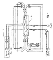
- FIG. 7 shows the preferred interconnection of the elements of FIG. 6 .
- the icon labelled Correlator_ 1 [101] ( 70 ) is taken to represent a set of 101 instances of the circuit elements of FIG. 6 , labels on the periphery of the icon 70 representing the wires with similar labels in FIG. 6 .
- An electronic schematic “bus construct” has been used to clarify the connectivity of the preferred embodiment shown here. Those skilled in the art will be familiar with these bus constructs, however more details are given here. Specifically, connections shown as a single line represent a single wire, connections shown as narrow rectangles represent a collection of wires or a “bus”. Slashed oblique lines with adjacent integers are taken to indicate the number of wires within the bus so marked.
- Lines emerging at 45 degrees from within the narrow bus rectangle are taken to indicate the means to “tap” into the bus—that is to say, the means by which certain of the particular wires within the bus may be accessed.
- the integer or pair of integers delimited by the colon character (:), are indicative of the particular wires within the bus that are accessed by the tap.
- a single integer at the tap indicates one of the wires within the bus by number, starting from zero. For example, a bus indicated to contain 101 elements by use of the slashed oblique line and associated integer will contain 101 individual wires that may be specified by index numbers 0 through 100.
- a delimited pair of integers, for example 3:0 is taken to indicate, in order, the wires with index 3 , index 2 , index 1 and index 0 .
- Element 70 is the iconic representation of the 101 instances of the circuit of FIG. 6 .
- icon 70 is attached to a bus of 101 wires, as is the case, for example in the peripheral area marked “Sample”, this is taken to represent the connection of each of the 101 wires within the bus to each of the 101 separate instances of the FIG. 6 wire labelled “Sample”.
- the icon 70 is attached to a single wire, as is the case in the peripheral area labelled “Ain”, that single wire is taken to connect to all of the wires labelled “Ain” within the 101 instances of the circuit of FIG. 6 . Consequently, it is clear that the analog input connects to all SHA elements 60 within FIG. 6 .
- the busses and the indices on the taps complete the connectivity.
- Aleft bus element index 0 is connected to Aright bus element index 100
- Aleft bus index 1 is similarly connected to Aright bus index 99
- the other connections, namely Aleft bus indices 100 down though to 2 are connected to Aright bus indices 98 down though to 0.
- Similar consideration applied to the wires Din and Doutb will show that they are connected in sequence from the first (0 th ) through to the last (100 th ) iteration of the elements of FIG. 6 .
- the wires labelled Sample are connected such that the Sample input to iteration Nth of the circuit of FIG.
- the construct “DGnd#100” is taken to indicate a connection of each of the 100 wires within the associated bus to the DGnd (ground) terminal.
- the presence of the Start terminal connected as shown is to provided for the application of a pulse, initially at a logical high level, which when taken to a logic low level, begins the sequence of delays generated in the circular connection of elements 62 .
- the collection of output wires shown in 71 is merged into a common pair of output wires to be considered output and inverse output. These wires provide for the function of a addition of the signals emerging on the Aout and Aoutb wires. The exact connection being made as Aout to output terminal, Aoutb to inverse output terminal; or as Aoutb to output terminal and Aout to inverse output terminal as required by the sign of the coefficient value as described above.
- FIG. 8 shows the results of a SPICE simulation of the circuit as described in FIGS. 6 and 7 .
- Coefficient values have been applied to the array such that 25 cycles of coefficient values occur within the 101 elements, the delay through the elements 62 is set to be 293.86 pS.
- the logically next output occurs in the gate 50 steps ahead in the sequence since that gate has just passed the inverse logic signal when compared to this example gate, hence it is the output of the gate 50 steps ahead in the chain that constitutes the logically next output in time. Therefore, the connection of the coefficients indexed by C n to the instances of the circuit in FIG. 6 is as follows. I n is taken to indicate the n instance in the chain as connected by Din and Doutb:
- Plot 80 is the time domain result in terms of the current difference between the current in the output terminal and the inverse output terminal.
- Plot 81 is a Fourier analysis of this signal showing the expected approximately 10 Mhz difference signal present at the output. [Other resonances shown, namely those at higher frequencies and below ⁇ 120 dB axis marker, are created due to non-linearities in the multiplier elements which are not the subject of this disclosure].
- the invention is therefore a system of interconnected analog components that continuously evaluates at least one sum of products.
- This sum of products represents the correlation of an apparent signal generated by the deliberate avoidance of advancing the coefficient weight with the signal pipeline.
- the process therefore differs from the prior art approaches to the discrete time approximation of a continuous integral because of the lack of advancing the coefficient pipeline.
- the invention is not limited to such applications.
- the invention would be implemented as parallel sets of arrays for the normal and quadrature channels with an RMS evaluation.
- the description herein includes the disclosure of a correlator wherein at least one of the signals to be correlated is created as a result of the sequential sampling adjacent to differing coefficients in the array. Such a correlator may be useful in a large number of applications.
Abstract
Description
R=√{square root over (S s ·S s +S c ·S c)}
where S s=Σn=0 m X n·sin(f·k·n),S c=Σn=0 m X n·cos(f·k·n)
H(ω)=∫−∞ ∞ X(t)·e j·ω·t dt
R=√{square root over (S s ·S s +S c ·S c)}
where S s=Σn=0 m X·sin(f·k·n),S c=Σn=0 m X n·cos(f·k·n)
. . . +Xn·sn+Xn+1·sn+1+Xn+2·sn+2+Xn+3·sn+3+ . . .
where the sn are the fixed (invariant for a particular receiver frequency) sine and cosine terms and the Xn are the samples of the input signal from the radio antenna.
Claims (13)
Priority Applications (1)
| Application Number | Priority Date | Filing Date | Title |
|---|---|---|---|
| US11/340,933 US8001172B2 (en) | 2001-01-29 | 2006-01-27 | High speed filter |
Applications Claiming Priority (4)
| Application Number | Priority Date | Filing Date | Title |
|---|---|---|---|
| CA2,332,609 | 2001-01-29 | ||
| CA002332609A CA2332609A1 (en) | 2001-01-29 | 2001-01-29 | High speed filter |
| US10/057,087 US7028070B2 (en) | 2001-01-29 | 2002-01-26 | High speed filter |
| US11/340,933 US8001172B2 (en) | 2001-01-29 | 2006-01-27 | High speed filter |
Related Parent Applications (1)
| Application Number | Title | Priority Date | Filing Date |
|---|---|---|---|
| US10/057,087 Continuation US7028070B2 (en) | 2001-01-29 | 2002-01-26 | High speed filter |
Publications (2)
| Publication Number | Publication Date |
|---|---|
| US20060123075A1 US20060123075A1 (en) | 2006-06-08 |
| US8001172B2 true US8001172B2 (en) | 2011-08-16 |
Family
ID=4168189
Family Applications (2)
| Application Number | Title | Priority Date | Filing Date |
|---|---|---|---|
| US10/057,087 Expired - Lifetime US7028070B2 (en) | 2001-01-29 | 2002-01-26 | High speed filter |
| US11/340,933 Expired - Fee Related US8001172B2 (en) | 2001-01-29 | 2006-01-27 | High speed filter |
Family Applications Before (1)
| Application Number | Title | Priority Date | Filing Date |
|---|---|---|---|
| US10/057,087 Expired - Lifetime US7028070B2 (en) | 2001-01-29 | 2002-01-26 | High speed filter |
Country Status (10)
| Country | Link |
|---|---|
| US (2) | US7028070B2 (en) |
| EP (1) | EP1356313B1 (en) |
| JP (1) | JP2004528742A (en) |
| CN (1) | CN100353179C (en) |
| AT (1) | ATE489771T1 (en) |
| AU (1) | AU2002243664A1 (en) |
| CA (1) | CA2332609A1 (en) |
| DE (1) | DE60238387D1 (en) |
| TW (1) | TW546919B (en) |
| WO (1) | WO2002060261A2 (en) |
Cited By (4)
| Publication number | Priority date | Publication date | Assignee | Title |
|---|---|---|---|---|
| WO2013067465A1 (en) | 2011-11-04 | 2013-05-10 | Ess Technology, Inc. | Down-conversion of multiple rf channels |
| EP2709282A2 (en) | 2012-09-12 | 2014-03-19 | Ess Technology, Inc. | Minimizing bandwidth in down-conversion of multiple RF channels |
| US20160006416A1 (en) * | 2014-07-03 | 2016-01-07 | Ess Technology, Inc. | Semi-Analog FIR Filter With High Impedance State |
| US20170111029A1 (en) * | 2015-10-14 | 2017-04-20 | Witricity Corporation | Phase and amplitude detection in wireless energy transfer systems |
Families Citing this family (13)
| Publication number | Priority date | Publication date | Assignee | Title |
|---|---|---|---|---|
| US6768372B2 (en) * | 2002-12-20 | 2004-07-27 | Intel Corporation | Analog filter architecture |
| US7680173B2 (en) * | 2005-07-06 | 2010-03-16 | Ess Technology, Inc. | Spread spectrum clock generator having an adjustable delay line |
| US7724805B1 (en) * | 2006-09-06 | 2010-05-25 | Rf Micro Devices, Inc. | Fast RMS measurement of input I/Q signals in a W-CDMA system |
| WO2010088293A2 (en) | 2009-01-28 | 2010-08-05 | Ess Technology, Inc. | Channel select filter apparatus and method |
| WO2011069229A1 (en) * | 2009-12-11 | 2011-06-16 | Ess Technology, Inc. | Virtual weaver architecture filter |
| WO2011071547A1 (en) * | 2009-12-11 | 2011-06-16 | Ess Technology, Inc. | Analog processing elements in a sum of products |
| CN102185587B (en) * | 2011-03-21 | 2013-07-24 | 浙江大学 | Low-power-consumption multi-order interpolation half-band filter with two-phase structure |
| US8504601B2 (en) | 2011-03-22 | 2013-08-06 | Ess Technology, Inc. | FIR filter with reduced element count |
| US9287851B2 (en) * | 2011-03-22 | 2016-03-15 | Ess Technology, Inc. | Finite impulse response filter for producing outputs having different phases |
| US9235499B2 (en) * | 2011-12-16 | 2016-01-12 | General Electric Company | System and method for identifying a character-of-interest |
| KR101878400B1 (en) * | 2017-02-06 | 2018-07-13 | 울산과학기술원 | FIR filter calculation method using approximate synthesis |
| CN110518894B (en) * | 2019-08-23 | 2023-01-03 | 极芯通讯技术(南京)有限公司 | High-speed low-complexity second-order all-pass filter |
| RU2735488C1 (en) * | 2020-04-03 | 2020-11-03 | Федеральное государственное бюджетное образовательное учреждение высшего образования "Майкопский государственный технологический университет" | Digital correlator |
Citations (31)
| Publication number | Priority date | Publication date | Assignee | Title |
|---|---|---|---|---|
| JPS5294051A (en) | 1976-01-30 | 1977-08-08 | Thomson Csf | Electric charge coupling type correlator |
| US4161033A (en) | 1977-12-22 | 1979-07-10 | Rca Corporation | Correlator/convolver using a second shift register to rotate sample values |
| US4318080A (en) | 1976-12-16 | 1982-03-02 | Hajime Industries, Ltd. | Data processing system utilizing analog memories having different data processing characteristics |
| EP0078674A2 (en) | 1981-10-29 | 1983-05-11 | American Microsystems, Incorporated | Programmable transversal filter and method of filtering a signal |
| US4403331A (en) | 1981-05-01 | 1983-09-06 | Microdyne Corporation | Method and apparatus for transmitting data over limited bandwidth channels |
| US4550415A (en) | 1983-11-16 | 1985-10-29 | At&T Bell Laboratories | Fractionally spaced equalization using nyquist-rate coefficient updating |
| US4580224A (en) | 1983-08-10 | 1986-04-01 | E. W. Bliss Company, Inc. | Method and system for generating an eccentricity compensation signal for gauge control of position control of a rolling mill |
| US4667203A (en) | 1982-03-01 | 1987-05-19 | Aero Service Div, Western Geophysical | Method and system for determining position using signals from satellites |
| US4860018A (en) | 1982-03-01 | 1989-08-22 | Western Atlas International, Inc. | Continuous wave interference rejection for reconstructed carrier receivers |
| US4870422A (en) | 1982-03-01 | 1989-09-26 | Western Atlas International, Inc. | Method and system for determining position from signals from satellites |
| US5014327A (en) | 1987-06-15 | 1991-05-07 | Digital Equipment Corporation | Parallel associative memory having improved selection and decision mechanisms for recognizing and sorting relevant patterns |
| US5021793A (en) | 1989-10-18 | 1991-06-04 | Unisys Corporation | Phased array antenna method and system for adaptively positioning nulls |
| US5027116A (en) | 1987-02-24 | 1991-06-25 | Micro Linear Corporation | Self-calibrating analog to digital converter |
| US5168213A (en) | 1990-03-13 | 1992-12-01 | Hewlett-Packard Company | Swept signal analysis instrument and method |
| US5194871A (en) | 1982-03-01 | 1993-03-16 | Western Atlas International, Inc. | System for simultaneously deriving position information from a plurality of satellite transmissions |
| US5353026A (en) | 1992-12-15 | 1994-10-04 | Analog Devices, Inc. | Fir filter with quantized coefficients and coefficient quantization method |
| US5438532A (en) | 1993-01-20 | 1995-08-01 | Sanyo Electric Co., Ltd. | Digital filter for use in synthesizing filter or a separation filter |
| US5463657A (en) | 1994-02-15 | 1995-10-31 | Lockheed Missiles & Space Company, Inc. | Detection of a multi-sequence spread spectrum signal |
| US5469469A (en) | 1993-12-07 | 1995-11-21 | University Of Massachusetts Lowell Research Foundation | Composite spread spectrum signal including modulator demodulator |
| US5537435A (en) | 1994-04-08 | 1996-07-16 | Carney; Ronald | Transceiver apparatus employing wideband FFT channelizer with output sample timing adjustment and inverse FFT combiner for multichannel communication network |
| US5563819A (en) | 1994-03-31 | 1996-10-08 | Cirrus Logic, Inc. | Fast high precision discrete-time analog finite impulse response filter |
| US5754603A (en) | 1995-08-03 | 1998-05-19 | Northern Telecom Limited | Pseudo random number sequence synchronization in communications systems |
| EP0903863A1 (en) | 1997-09-19 | 1999-03-24 | Motorola, Inc. | One-bit analog-to-digital converter |
| US5901075A (en) | 1995-12-22 | 1999-05-04 | Lucent Technologies Inc. | Performance of an adaptive weight FIR filter having a timeshared tap weight processor |
| US5914983A (en) | 1994-09-06 | 1999-06-22 | Matsushita Electric Industrial Co., Ltd. | Digital signal error reduction apparatus |
| US5999561A (en) | 1997-05-20 | 1999-12-07 | Sanconix, Inc. | Direct sequence spread spectrum method, computer-based product, apparatus and system tolerant to frequency reference offset |
| US6032171A (en) | 1995-01-04 | 2000-02-29 | Texas Instruments Incorporated | Fir filter architecture with precise timing acquisition |
| US6111911A (en) | 1995-06-07 | 2000-08-29 | Sanconix, Inc | Direct sequence frequency ambiguity resolving receiver |
| US6141373A (en) | 1996-11-15 | 2000-10-31 | Omnipoint Corporation | Preamble code structure and detection method and apparatus |
| US6154486A (en) | 1995-06-05 | 2000-11-28 | Omnipoint Corporation | Preamble code structure and detection method and apparatus |
| US6718355B2 (en) | 2001-02-05 | 2004-04-06 | Conexant Systems, Inc. | Systems and methods for a partial sum digital fir filter |
Family Cites Families (2)
| Publication number | Priority date | Publication date | Assignee | Title |
|---|---|---|---|---|
| US5414729A (en) * | 1992-01-24 | 1995-05-09 | Novatel Communications Ltd. | Pseudorandom noise ranging receiver which compensates for multipath distortion by making use of multiple correlator time delay spacing |
| JP3092828B2 (en) * | 1992-04-30 | 2000-09-25 | 株式会社日立製作所 | Soldering inspection method and apparatus by X-ray transmission image detection |
-
2001
- 2001-01-29 CA CA002332609A patent/CA2332609A1/en not_active Abandoned
-
2002
- 2002-01-26 US US10/057,087 patent/US7028070B2/en not_active Expired - Lifetime
- 2002-01-26 WO PCT/US2002/002172 patent/WO2002060261A2/en active Application Filing
- 2002-01-26 EP EP02709164A patent/EP1356313B1/en not_active Expired - Lifetime
- 2002-01-26 AT AT02709164T patent/ATE489771T1/en not_active IP Right Cessation
- 2002-01-26 JP JP2002560465A patent/JP2004528742A/en active Pending
- 2002-01-26 DE DE60238387T patent/DE60238387D1/en not_active Expired - Lifetime
- 2002-01-26 AU AU2002243664A patent/AU2002243664A1/en not_active Abandoned
- 2002-01-26 CN CNB028042506A patent/CN100353179C/en not_active Expired - Fee Related
- 2002-01-29 TW TW091101417A patent/TW546919B/en not_active IP Right Cessation
-
2006
- 2006-01-27 US US11/340,933 patent/US8001172B2/en not_active Expired - Fee Related
Patent Citations (34)
| Publication number | Priority date | Publication date | Assignee | Title |
|---|---|---|---|---|
| US4103333A (en) | 1976-01-30 | 1978-07-25 | Thomson-Csf | Charge coupled correlator device |
| JPS5294051A (en) | 1976-01-30 | 1977-08-08 | Thomson Csf | Electric charge coupling type correlator |
| US4318080A (en) | 1976-12-16 | 1982-03-02 | Hajime Industries, Ltd. | Data processing system utilizing analog memories having different data processing characteristics |
| US4161033A (en) | 1977-12-22 | 1979-07-10 | Rca Corporation | Correlator/convolver using a second shift register to rotate sample values |
| US4403331A (en) | 1981-05-01 | 1983-09-06 | Microdyne Corporation | Method and apparatus for transmitting data over limited bandwidth channels |
| EP0078674A2 (en) | 1981-10-29 | 1983-05-11 | American Microsystems, Incorporated | Programmable transversal filter and method of filtering a signal |
| US4475170A (en) | 1981-10-29 | 1984-10-02 | American Microsystems, Inc. | Programmable transversal filter |
| US5194871A (en) | 1982-03-01 | 1993-03-16 | Western Atlas International, Inc. | System for simultaneously deriving position information from a plurality of satellite transmissions |
| US5384574A (en) | 1982-03-01 | 1995-01-24 | Western Atlas International, Inc. | System for determining position from suppressed carrier radio waves |
| US4667203A (en) | 1982-03-01 | 1987-05-19 | Aero Service Div, Western Geophysical | Method and system for determining position using signals from satellites |
| US4860018A (en) | 1982-03-01 | 1989-08-22 | Western Atlas International, Inc. | Continuous wave interference rejection for reconstructed carrier receivers |
| US4870422A (en) | 1982-03-01 | 1989-09-26 | Western Atlas International, Inc. | Method and system for determining position from signals from satellites |
| US4580224A (en) | 1983-08-10 | 1986-04-01 | E. W. Bliss Company, Inc. | Method and system for generating an eccentricity compensation signal for gauge control of position control of a rolling mill |
| US4550415A (en) | 1983-11-16 | 1985-10-29 | At&T Bell Laboratories | Fractionally spaced equalization using nyquist-rate coefficient updating |
| US5027116A (en) | 1987-02-24 | 1991-06-25 | Micro Linear Corporation | Self-calibrating analog to digital converter |
| US5014327A (en) | 1987-06-15 | 1991-05-07 | Digital Equipment Corporation | Parallel associative memory having improved selection and decision mechanisms for recognizing and sorting relevant patterns |
| US5021793A (en) | 1989-10-18 | 1991-06-04 | Unisys Corporation | Phased array antenna method and system for adaptively positioning nulls |
| US5168213A (en) | 1990-03-13 | 1992-12-01 | Hewlett-Packard Company | Swept signal analysis instrument and method |
| US5353026A (en) | 1992-12-15 | 1994-10-04 | Analog Devices, Inc. | Fir filter with quantized coefficients and coefficient quantization method |
| US5438532A (en) | 1993-01-20 | 1995-08-01 | Sanyo Electric Co., Ltd. | Digital filter for use in synthesizing filter or a separation filter |
| US5469469A (en) | 1993-12-07 | 1995-11-21 | University Of Massachusetts Lowell Research Foundation | Composite spread spectrum signal including modulator demodulator |
| US5463657A (en) | 1994-02-15 | 1995-10-31 | Lockheed Missiles & Space Company, Inc. | Detection of a multi-sequence spread spectrum signal |
| US5563819A (en) | 1994-03-31 | 1996-10-08 | Cirrus Logic, Inc. | Fast high precision discrete-time analog finite impulse response filter |
| US5537435A (en) | 1994-04-08 | 1996-07-16 | Carney; Ronald | Transceiver apparatus employing wideband FFT channelizer with output sample timing adjustment and inverse FFT combiner for multichannel communication network |
| US5914983A (en) | 1994-09-06 | 1999-06-22 | Matsushita Electric Industrial Co., Ltd. | Digital signal error reduction apparatus |
| US6032171A (en) | 1995-01-04 | 2000-02-29 | Texas Instruments Incorporated | Fir filter architecture with precise timing acquisition |
| US6154486A (en) | 1995-06-05 | 2000-11-28 | Omnipoint Corporation | Preamble code structure and detection method and apparatus |
| US6111911A (en) | 1995-06-07 | 2000-08-29 | Sanconix, Inc | Direct sequence frequency ambiguity resolving receiver |
| US5754603A (en) | 1995-08-03 | 1998-05-19 | Northern Telecom Limited | Pseudo random number sequence synchronization in communications systems |
| US5901075A (en) | 1995-12-22 | 1999-05-04 | Lucent Technologies Inc. | Performance of an adaptive weight FIR filter having a timeshared tap weight processor |
| US6141373A (en) | 1996-11-15 | 2000-10-31 | Omnipoint Corporation | Preamble code structure and detection method and apparatus |
| US5999561A (en) | 1997-05-20 | 1999-12-07 | Sanconix, Inc. | Direct sequence spread spectrum method, computer-based product, apparatus and system tolerant to frequency reference offset |
| EP0903863A1 (en) | 1997-09-19 | 1999-03-24 | Motorola, Inc. | One-bit analog-to-digital converter |
| US6718355B2 (en) | 2001-02-05 | 2004-04-06 | Conexant Systems, Inc. | Systems and methods for a partial sum digital fir filter |
Non-Patent Citations (3)
| Title |
|---|
| European Search Report dated Mar. 24, 2009 for a corresponding European Application No. 02709164.4. |
| K. Muhammed, et. al., A Discrete-Time Bluetooth Receiver in a 0.13 m Digitial CMOS Process, 2004 ISSCC, Session 15, Wireless Consumer ICs Texas Instruments, Dallas TX. |
| N.I. Kaushanskiy "Synthesis of Frequency Characteristics by Means of a Tapped Delay Line" Telecommunications and Radio Engineering, Sep. 1967, pp. 80-86. |
Cited By (7)
| Publication number | Priority date | Publication date | Assignee | Title |
|---|---|---|---|---|
| WO2013067465A1 (en) | 2011-11-04 | 2013-05-10 | Ess Technology, Inc. | Down-conversion of multiple rf channels |
| US8693972B2 (en) | 2011-11-04 | 2014-04-08 | Ess Technology, Inc. | Down-conversion of multiple RF channels |
| EP2709282A2 (en) | 2012-09-12 | 2014-03-19 | Ess Technology, Inc. | Minimizing bandwidth in down-conversion of multiple RF channels |
| US20160006416A1 (en) * | 2014-07-03 | 2016-01-07 | Ess Technology, Inc. | Semi-Analog FIR Filter With High Impedance State |
| US9647640B2 (en) * | 2014-07-03 | 2017-05-09 | Ess Technology, Inc. | Semi-analog FIR filter with high impedance state |
| US20170111029A1 (en) * | 2015-10-14 | 2017-04-20 | Witricity Corporation | Phase and amplitude detection in wireless energy transfer systems |
| US9929721B2 (en) * | 2015-10-14 | 2018-03-27 | Witricity Corporation | Phase and amplitude detection in wireless energy transfer systems |
Also Published As
| Publication number | Publication date |
|---|---|
| TW546919B (en) | 2003-08-11 |
| WO2002060261A3 (en) | 2002-10-17 |
| AU2002243664A1 (en) | 2002-08-12 |
| CA2332609A1 (en) | 2002-07-29 |
| ATE489771T1 (en) | 2010-12-15 |
| EP1356313A2 (en) | 2003-10-29 |
| US7028070B2 (en) | 2006-04-11 |
| CN1489701A (en) | 2004-04-14 |
| EP1356313B1 (en) | 2010-11-24 |
| US20020129070A1 (en) | 2002-09-12 |
| DE60238387D1 (en) | 2011-01-05 |
| WO2002060261A2 (en) | 2002-08-08 |
| US20060123075A1 (en) | 2006-06-08 |
| CN100353179C (en) | 2007-12-05 |
| JP2004528742A (en) | 2004-09-16 |
| EP1356313A4 (en) | 2009-04-22 |
Similar Documents
| Publication | Publication Date | Title |
|---|---|---|
| US8001172B2 (en) | High speed filter | |
| US5523758A (en) | Sliding correlator for nanosecond pulses | |
| Rice et al. | Quadrature sampling with high dynamic range | |
| EP0254844B1 (en) | Digital pipelined heterodyne circuit | |
| US8548100B2 (en) | Method and system for performing complex sampling of signals by using two or more sampling channels and for calculating time delays between these channels | |
| EP1789810B1 (en) | Method and apparatus for measuring the frequency of a received signal | |
| EP0131260A2 (en) | An arrangement to provide an accurate time-of-arrival indication for a received signal | |
| JP2008271530A (en) | Analog-to-digital converter system | |
| WO2008118343A1 (en) | Analog-to-digital converter system with increased sampling frequency | |
| Eklund et al. | A multiple sampling, single A/D conversion technique for I/Q demodulation in CMOS | |
| US4947408A (en) | Digital carrier demodulator employing components working beyond normal limits | |
| JP3122104B2 (en) | Variable rate square matched filter | |
| JPH0588571B2 (en) | ||
| US6738435B1 (en) | Matched-filter frequency-shift-keyed receiver using degenerate digital signal processing techniques | |
| US6518908B2 (en) | Method and device for analog-to-digital conversion of a signal | |
| US4016567A (en) | CCD range-doppler processor | |
| Kwentus et al. | A 250 Msample/sec programmable cascaded integrator-comb decimation filter | |
| JPH0865107A (en) | Digital interpolation filter circuit | |
| AU2011241819A1 (en) | Implementation of complex sampling and time delays calculation | |
| Gopen | Telecommunication Applications for CTD Devices | |
| GB2073979A (en) | Digital-to-analog converter deglitching circuit | |
| US6801605B1 (en) | Telephone network signal conversion system | |
| JPH0697775A (en) | Digital matched filter | |
| JP3300806B2 (en) | Matched filter | |
| Wang | Switched-current circuit design techniques for signal processing |
Legal Events
| Date | Code | Title | Description |
|---|---|---|---|
| AS | Assignment |
Owner name: THE PRIVATE BANK OF THE PENINSULA, CALIFORNIA Free format text: SECURITY AGREEMENT;ASSIGNOR:ESS TECHNOLOGY, INC.;REEL/FRAME:021212/0413 Effective date: 20080703 Owner name: THE PRIVATE BANK OF THE PENINSULA,CALIFORNIA Free format text: SECURITY AGREEMENT;ASSIGNOR:ESS TECHNOLOGY, INC.;REEL/FRAME:021212/0413 Effective date: 20080703 |
|
| ZAAA | Notice of allowance and fees due |
Free format text: ORIGINAL CODE: NOA |
|
| ZAAB | Notice of allowance mailed |
Free format text: ORIGINAL CODE: MN/=. |
|
| STCF | Information on status: patent grant |
Free format text: PATENTED CASE |
|
| REMI | Maintenance fee reminder mailed | ||
| FPAY | Fee payment |
Year of fee payment: 4 |
|
| SULP | Surcharge for late payment | ||
| FEPP | Fee payment procedure |
Free format text: MAINTENANCE FEE REMINDER MAILED (ORIGINAL EVENT CODE: REM.); ENTITY STATUS OF PATENT OWNER: LARGE ENTITY |
|
| FEPP | Fee payment procedure |
Free format text: 7.5 YR SURCHARGE - LATE PMT W/IN 6 MO, LARGE ENTITY (ORIGINAL EVENT CODE: M1555); ENTITY STATUS OF PATENT OWNER: LARGE ENTITY |
|
| MAFP | Maintenance fee payment |
Free format text: PAYMENT OF MAINTENANCE FEE, 8TH YEAR, LARGE ENTITY (ORIGINAL EVENT CODE: M1552); ENTITY STATUS OF PATENT OWNER: LARGE ENTITY Year of fee payment: 8 |
|
| FEPP | Fee payment procedure |
Free format text: MAINTENANCE FEE REMINDER MAILED (ORIGINAL EVENT CODE: REM.); ENTITY STATUS OF PATENT OWNER: LARGE ENTITY |
|
| LAPS | Lapse for failure to pay maintenance fees |
Free format text: PATENT EXPIRED FOR FAILURE TO PAY MAINTENANCE FEES (ORIGINAL EVENT CODE: EXP.); ENTITY STATUS OF PATENT OWNER: LARGE ENTITY |
|
| STCH | Information on status: patent discontinuation |
Free format text: PATENT EXPIRED DUE TO NONPAYMENT OF MAINTENANCE FEES UNDER 37 CFR 1.362 |
|
| FP | Lapsed due to failure to pay maintenance fee |
Effective date: 20230816 |