US8098707B2 - Ultra wideband receiver - Google Patents
Ultra wideband receiver Download PDFInfo
- Publication number
- US8098707B2 US8098707B2 US11/669,938 US66993807A US8098707B2 US 8098707 B2 US8098707 B2 US 8098707B2 US 66993807 A US66993807 A US 66993807A US 8098707 B2 US8098707 B2 US 8098707B2
- Authority
- US
- United States
- Prior art keywords
- block
- signal
- coupled
- ultra wideband
- wideband receiver
- Prior art date
- Legal status (The legal status is an assumption and is not a legal conclusion. Google has not performed a legal analysis and makes no representation as to the accuracy of the status listed.)
- Active, expires
Links
Images


Classifications
-
- H—ELECTRICITY
- H04—ELECTRIC COMMUNICATION TECHNIQUE
- H04B—TRANSMISSION
- H04B1/00—Details of transmission systems, not covered by a single one of groups H04B3/00 - H04B13/00; Details of transmission systems not characterised by the medium used for transmission
- H04B1/69—Spread spectrum techniques
- H04B1/7163—Spread spectrum techniques using impulse radio
- H04B1/71637—Receiver aspects
Definitions
- the embodiments relate generally to data transmission and reception and more particularly to a non-coherent ultra wideband receiver.
- the transmitted signal comes to antenna and pass through band pass filter (BPF).
- BPF band pass filter
- the signal is fed into X n (n>1) device.
- the output signal from the X n (n>1) device is fed into integration/dump block.
- the output from the integration/dump block is fed into decision block.
- Single or multiple short pulse(s), impulse(s) or ultra-wideband signal(s) represent a data.
- the transmitted short pulse(s), impulse(s) or ultra-wideband signal(s) representing a data is (are) confined in a fixed time period (Tb).
- the integration time (Tin) for the integration/dump block may be equal to or smaller than Tb, and greater than or equal to each pulse, impulse or ultra-wideband signal duration time.
- Some embodiments use a non-coherent type receiver that makes the system simple and easy to implement.
- Some embodiments use an X n (n>1) device.
- a simple multiplier can be used as a X2 device.
- a simple comparator can be used as a decision making device for the receiver in some embodiments.
- another embodiment of this invention uses integration/dump block to further improve the decision accuracy and provide system versatility.
- Another feature of some embodiments is the use of a short integration time as described below to implement receiver performance.
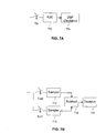
- FIGS. 1A and 1B show pulse, impulse or ultra-wide-band signal receiver architectures according to embodiments of the invention.
- FIGS. 2A and 2B show pulse, impulse or ultra-wide-band signal receiver architectures according to alternative embodiments of the invention.
- FIGS. 3A and 3B show pulse, impulse or ultra-wide-band signal receiver architectures according to further alternative embodiments of the invention.
- FIGS. 4A and 4B provided further details of an X n block used in some embodiments of the invention.
- FIG. 5 shows an example multiplier circuit designed using CMOS technology that may be used in some embodiments.
- FIGS. 6A and 6B show example signal timing diagrams for a binary PPM (pulse position modulation) case
- FIGS. 7A and 7B provide further details of example dump switch and decision blocks according to embodiments of the invention.
- FIGS. 8A-8D show a simulation example of signals at various stages of the operation of receiver architectures according to embodiments of the invention.
- FIG. 9 illustrates a signal decision boundary for transmitted and received signals.
- FIGS. 10A-10D shows a BER (bit error rate) for the simulation results according to a particular embodiment.
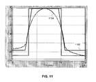
- FIG. 11 shows the frequency domain transfer function of the BPFs used in the simulation and according to a particular embodiment.
- the functions or algorithms described herein are implemented in hardware, and/or software in embodiments.
- the software comprises computer executable instructions stored on computer readable media such as memory or other types of storage devices.
- computer readable media is also used to represent software-transmitted carrier waves.
- modules which are software, hardware, firmware, or any combination thereof Multiple functions are performed in one or more modules as desired, and the embodiments described are merely examples.
- a digital signal processor, ASIC, microprocessor, or any other type of processor operating on a system, such as a personal computer, server, a router, or any other device capable of processing data including network interconnection devices executes the software.
- a block or module as described below may be implemented as logic, circuitry, or software that implements the functionality described for the block
- Some embodiments implement functions in two or more specific interconnected hardware modules or devices with related control and data signals communicated between and through the modules, or as portions of an application-specific integrated circuit.
- the example process flow is applicable to software, firmware, and hardware implementations.
- FIGS. 1A and 1B show pulse, impulse or ultra-wide-band signal receiver architectures 100 and 150 according to embodiments of the invention.
- a receiver 102 has band pass filter (BPF) 108 that passes signal spectrum.
- the BPF 108 may be further optimized by making the magnitude response of the filter to be similar with that of the power spectrum density of the incoming signal in the frequency domain.
- the BPF 108 can be located before ( FIG. 1B ) or after ( FIG. 1A ) a Transmit/Receive Switch (“T/R SW”) block 106 .
- the T/R SW block 106 may be omitted for frequency division (or hopping) multiplexing embodiments.
- the signal may be passed through an optional amplifier block 110 .
- the amplifier block 110 may be integrated with a following X n or e X block 112 (also referred to as a multiplier block).
- An e X block 112 is a device that receives an input and provides an output such that when the input is X, the output is approximately ⁇ Be X , where B is constant.
- An integration and dump block integrates the input signal for a certain time period (T in ) and dumps (sends) the integrated results to the following block.
- a decision block 116 receives the signal from integration and dump block 114 and makes decision as to whether the data is 0 or 1 using the dumped signals from the previous block.
- Transmitter 118 may optionally be used to provide for bi-directional communications with other wireless devices.
- FIGS. 2A and 2B show signal receiver architectures according to alternative embodiments of the invention.
- the receiver may be a pulse, impulse or ultra-wide-band signal receiver architecture.
- the receiver architectures 200 and 250 illustrated in FIGS. 2A and 2B respectively are similar to the architecture illustrated in FIGS. 1A and 1B .
- Receiver architectures 200 and 250 include a rectifier or envelope detector 202 inserted at the front of the X n or e X block 112 .
- the amplifier and rectifier (or envelope detector) location may be switched.
- the amplifier 110 may be combined with rectifier (or envelope detector) 202 or X n (or e X ) block 112 .
- n can be any number bigger than 1.
- FIGS. 3A and 3B show pulse, impulse or ultra-wide-band signal receiver architectures 300 and 350 according to further alternative embodiments of the invention.
- the receiver architectures 300 and 350 illustrated in FIGS. 3A and 3B are similar to those illustrated in FIGS. 1A and 1B .
- a comparator 302 is used instead of integration/dump block 114 .
- the comparator 302 compares the output from X n (or e X ) block 112 with a reference voltage Vref, and generates a detected output signal.
- n can be any number bigger than 1.
- FIGS. 4A and 4B provided further details of an X n block 112 used in some embodiments of the invention.
- the X n block 112 is an X 2 device.
- FIG. 4A shows one example of an X 2 block.
- a signal divider 404 splits the input signal and the multiplier 402 multiplies the divided signals. Instead of using a signal divider, the signal can be directly connected to both of the two inputs of a multiplier as illustrated in FIG. 4B .
- FIG. 5 shows an example multiplier circuit designed using CMOS technology that may be used in some embodiments.
- M 1 and M 2 may be nMOS transistors.
- the output from the multiplier (X 2 ) can be multiplied with the input signal (X) again to get X 3 .
- the X 2 device can be cascaded to get higher order outputs (X 4 , X 6 , . . . ). Further, it should be noted that The X n device and e X device can be combined in any sequence to get higher order outputs.
- FIGS. 6A and 6B show example signal timing diagrams for a binary PPM (pulse position modulation) case.
- the symbol time (Ts) is divided by two.
- the pulse(s) When the pulse(s) is located in the left half (Tb), the pulse represents a binary 0.
- the pulse(s) is located in the right half (Tb), the pulse represents a binary 1.
- the signal After passing X n or e X block 112 , the signal is integrated for time interval Tin.
- Tin may be equal to Tb or smaller than Tb.
- the integrated values for the left half (INT 0 ) and the right half (INT 0 ) are sent to the following stage. The following stage subtracts them and determines whether the pulse represents a 1 or 0.
- FIGS. 6A and 6B show binary PPM (pulse position modulation) case, but in varying embodiments the modulation can be PPM, PAM (pulse amplitude modulation) or OOK (on off keying). Further, in the interest of clarity and brevity, the example has only one bit per symbol. Those of skill in the art will appreciate that there can be any number of bits per symbol (M-ary system) and within the scope of the inventive subject matter. Still further, the example illustrated in FIGS. 6A and 6B shows a single pulse per binary time. Those of skill in the art will appreciate that multiple pulses per binary (or M-Ary) time is possible and within the scope of the inventive subject matter.
- FIGS. 7A and 7B provide further details of example dump switch and decision blocks according to embodiments of the invention.
- an ADC 702 converts the dumped signals into digital signals
- the digital signal-processing block 704 makes decision based on the dumped and AD converted signals.
- the left half (Tin 0 ) integrated signal (INT 0 ) and the right half (Tin 1 ) integrated signal (INT 1 ) are sampled separately by samplers 710 and subtracted at the following stage 712 to make decision 714 .
- FIGS. 8A-8D show a simulation example of signals at various stages of the operation of the above-described architectures.
- FIG. 8A shows an example input signal to the receiver 102 that has pulse position modulated signal and noise.
- FIG. 8B shows the signal after passing BPF 108 . Any kind of BPF 108 may be used. In some embodiments, a BPF whose magnitude response is close to that of the power spectrum density of an input signal is desirable and may improve the system performance.
- FIG. 8C shows the signal after passing an X 2 block 112 . The example signal becomes peakier and this peaky signal may improve the receiver performance.
- FIG. 8D shows the example signal at the integration and dump block 114 . In the example shown, the integration time (Tin) is half of the binary time (Tb). The dumped signal is sent to ADC 702 , and the left half integrated signal (INT 0 ) and the right half integrated signal (INT 1 ) are subtracted (INT 0 -INT 1 ).
- FIG. 9 illustrates a signal decision boundary for transmitted and received signals.
- the decision boundary is 0. If “INT 0 -INT 1 ” is above the decision boundary the recovered data is 1. If “INT 0 -INT 1 ” is below the decision boundary the recovered data is 0.
- the dashed line 902 is the data sent at the transmitter side, and solid line 904 is the data recovered at the receiver side.
- FIGS. 10A-10D shows a BER (bit error rate) for the simulation results according to a particular embodiment.
- FIG. 10A compares the performance of a simple rectifier based non-coherent detector and that of the X n block based non-coherent receiver 102 (X 2 case).
- the X-axis is SNR (signal to noise ratio) and Y-axis is BER (bit error rate).
- SNR signal to noise ratio
- BER bit error rate
- FIG. 10B compares the performance of a coherent detector and that of the novel X n block based non-coherent receiver (X 2 case) that has a typical BPF and integration time (Tin) equal to binary time (Tb) according to a particular embodiment.
- X 2 case the novel X n block based non-coherent receiver
- Tin binary time
- Tb binary time
- the input signal is multiplied with a template signal.
- the template signal When the template signal is ideal, it shows better performance than X 2 based non-coherent receiver. But the template signal generally can't be ideal.
- a synchronization error between input signal and template signal, non-ideal template signal shape and noise in the template signal break down the performance of a coherent receiver.
- the novel receiver of the embodiments of the invention doesn't use a template signal, and therefore doesn't suffer those problems.
- FIG. 10B compares the performance of a coherent detector and that of the novel X n block based non-coherent receiver (
- Template generation circuit design is not trivial. Usually it requires expensive high performance technology like BiCMOS or GaAs, and it consumes lots of power. Because the novel receiver of various embodiment doesn't need to generate a template signal, the design of some embodiments may be less expensive and easier-to-implement and further may make a low power design possible.
- FIG. 10C shows that reducing the integration time improves the receiver performance further.
- FIG. 10D compares the performance of a coherent detector and that of the novel X n block based non-coherent receiver (X 2 case) that has optimized BPF and integration time (Tin) equal to binary time (Tb) according to a particular embodiment. Making the magnitude response of a BPF close to the power spectrum density of incoming signal may optimize the BPF. FIG. 10D shows that using such and optimized BPF improves the receiver performance further.
- FIG. 11 shows the frequency domain transfer function of the BPFs used in the simulation and according to a particular embodiment.
- the line 1102 is for a typical BPF 108 and the line 1 104 is for a BPF 108 that has same magnitude response with the incoming signals power spectrum density.
- the receiver including an X n device and integrator described above provides a method that does not require exact timing. Because the exact pulse position may not be known, the receiver of the various embodiments obtains the approximate peak based on the average by using the X n device and Integrator instead of sampling the signal at the exact peak. Thus some embodiments may provide for the elimination of the template signal generator and timing control blocks that consume a significant portion of the power used in conventional receivers. Further, in some embodiments, the degradation in performance is limited in comparison to a conventional coherent receiver that includes the effect of jitter.
- Apps that may include the apparatus and systems of various embodiments broadly include a variety of electronic and computer systems.
- the elements, materials, geometries, dimensions, and sequence of operations can all be varied to suit particular packaging requirements.
Abstract
Description
Claims (16)
Priority Applications (1)
| Application Number | Priority Date | Filing Date | Title |
|---|---|---|---|
| US11/669,938 US8098707B2 (en) | 2006-01-31 | 2007-01-31 | Ultra wideband receiver |
Applications Claiming Priority (2)
| Application Number | Priority Date | Filing Date | Title |
|---|---|---|---|
| US74319806P | 2006-01-31 | 2006-01-31 | |
| US11/669,938 US8098707B2 (en) | 2006-01-31 | 2007-01-31 | Ultra wideband receiver |
Publications (2)
| Publication Number | Publication Date |
|---|---|
| US20070242735A1 US20070242735A1 (en) | 2007-10-18 |
| US8098707B2 true US8098707B2 (en) | 2012-01-17 |
Family
ID=38604814
Family Applications (1)
| Application Number | Title | Priority Date | Filing Date |
|---|---|---|---|
| US11/669,938 Active 2030-04-11 US8098707B2 (en) | 2006-01-31 | 2007-01-31 | Ultra wideband receiver |
Country Status (1)
| Country | Link |
|---|---|
| US (1) | US8098707B2 (en) |
Cited By (4)
| Publication number | Priority date | Publication date | Assignee | Title |
|---|---|---|---|---|
| US20140050252A1 (en) * | 2012-08-14 | 2014-02-20 | Tsinghua University | Apparatus and method for ultra wideband communication using dual band pass filter |
| WO2014177572A1 (en) | 2013-05-02 | 2014-11-06 | Ihp Gmbh - Innovations For High Performance Microelectronics / Leibniz-Institut Für Innovative Mikroelektronik | Receiver, arrangement, and method for ultra-broadband transmission |
| US10396849B1 (en) * | 2018-05-15 | 2019-08-27 | Qatar University | Non-coherent ultra-wideband receiver |
| WO2023239205A1 (en) * | 2022-06-10 | 2023-12-14 | Samsung Electronics Co., Ltd. | Method and device for inference in ultra-wide band system (uwb) |
Families Citing this family (4)
| Publication number | Priority date | Publication date | Assignee | Title |
|---|---|---|---|---|
| FI20115959A0 (en) * | 2011-09-30 | 2011-09-30 | Oulun Yliopisto | Information on modulation method |
| FI20115956A0 (en) * | 2011-09-30 | 2011-09-30 | Oulun Yliopisto | Transmission of data by ultra-wideband technology |
| KR101658933B1 (en) * | 2015-02-27 | 2016-09-22 | 전자부품연구원 | Impulse carrier recovery and uwb receiver included the recovery |
| US11502716B2 (en) * | 2020-12-16 | 2022-11-15 | Texas Instruments Incorporated | On-off keying receivers |
Citations (99)
| Publication number | Priority date | Publication date | Assignee | Title |
|---|---|---|---|---|
| US2671896A (en) | 1942-12-18 | 1954-03-09 | Itt | Random impulse system |
| US3587107A (en) | 1969-06-11 | 1971-06-22 | Sperry Rand Corp | Time limited impulse response antenna |
| US3612899A (en) | 1970-08-20 | 1971-10-12 | Sperry Rand Corp | Generator for short-duration high-frequency pulse signals |
| US3662316A (en) | 1971-03-12 | 1972-05-09 | Sperry Rand Corp | Short base-band pulse receiver |
| US3668639A (en) | 1971-05-07 | 1972-06-06 | Itt | Sequency filters based on walsh functions for signals with three space variables |
| US3678204A (en) | 1970-10-26 | 1972-07-18 | Itt | Signal processing and transmission by means of walsh functions |
| US3705981A (en) | 1970-10-05 | 1972-12-12 | Itt | Sequency filters based on walsh functions for signals with two space variables |
| US3728632A (en) | 1971-03-12 | 1973-04-17 | Sperry Rand Corp | Transmission and reception system for generating and receiving base-band pulse duration pulse signals without distortion for short base-band communication system |
| US3739392A (en) | 1971-07-29 | 1973-06-12 | Sperry Rand Corp | Base-band radiation and reception system |
| US3772697A (en) | 1971-04-19 | 1973-11-13 | Sperry Rand Corp | Base-band pulse object sensor system |
| US3806795A (en) | 1972-01-03 | 1974-04-23 | Geophysical Survey Sys Inc | Geophysical surveying system employing electromagnetic impulses |
| US3878749A (en) | 1972-12-12 | 1975-04-22 | Allen Organ Co | Walsh function tone generator and system |
| US3934252A (en) | 1974-04-08 | 1976-01-20 | Sperry Rand Corporation | Closed loop tunnel diode receiver for operation with a base band semiconductor transmitter |
| US4008469A (en) | 1974-08-06 | 1977-02-15 | Terrestrial Systems, Incorporated | Signal processing in short-pulse geophysical radar system |
| US4017854A (en) | 1975-08-21 | 1977-04-12 | Sperry Rand Corporation | Apparatus for angular measurement and beam forming with baseband radar systems |
| US4072942A (en) | 1976-02-20 | 1978-02-07 | Calspan Corporation | Apparatus for the detection of buried objects |
| US4099118A (en) | 1977-07-25 | 1978-07-04 | Franklin Robert C | Electronic wall stud sensor |
| US4152701A (en) | 1978-04-20 | 1979-05-01 | Sperry Rand Corporation | Base band speed sensor |
| US4254418A (en) | 1978-08-23 | 1981-03-03 | Sperry Corporation | Collision avoidance system using short pulse signal reflectometry |
| US4344705A (en) | 1979-03-07 | 1982-08-17 | Endress U. Hauser Gmbh U. Co. | Distance measuring apparatus based on the pulse travel time method |
| US4641317A (en) | 1984-12-03 | 1987-02-03 | Charles A. Phillips | Spread spectrum radio transmission system |
| US4651152A (en) | 1983-09-26 | 1987-03-17 | Geophysical Survey Systems, Inc. | Large relative bandwidth radar |
| US4688041A (en) | 1981-10-08 | 1987-08-18 | Sperry Corporation | Baseband detector with anti-jam capability |
| US4695752A (en) | 1982-01-11 | 1987-09-22 | Sperry Corporation | Narrow range gate baseband receiver |
| US4743906A (en) | 1984-12-03 | 1988-05-10 | Charles A. Phillips | Time domain radio transmission system |
| US4751515A (en) | 1980-07-09 | 1988-06-14 | Corum James F | Electromagnetic structure and method |
| US4813057A (en) | 1984-12-03 | 1989-03-14 | Charles A. Phillips | Time domain radio transmission system |
| US4862174A (en) | 1986-11-19 | 1989-08-29 | Natio Yoshiyuki | Electromagnetic wave absorber |
| US4907001A (en) | 1987-08-21 | 1990-03-06 | Geophysical Survey Systems, Inc. | Extraction of radar targets from clutter |
| US5057846A (en) | 1990-03-26 | 1991-10-15 | Geophysical Survey Systems, Inc. | Efficient operation of probing radar in absorbing media |
| US5095312A (en) | 1991-04-12 | 1992-03-10 | The United States Of America As Represented By The Secretary Of The Navy | Impulse transmitter and quantum detection radar system |
| US5134408A (en) | 1991-01-30 | 1992-07-28 | Geophysical Survey Systems, Inc. | Detection of radar signals with large radar signatures |
| US5146616A (en) | 1991-06-27 | 1992-09-08 | Hughes Aircraft Company | Ultra wideband radar transmitter employing synthesized short pulses |
| US5148175A (en) | 1991-07-05 | 1992-09-15 | Sperry Marine Inc. | High resolution variable range gate generator with programmable timing |
| US5148174A (en) | 1991-02-13 | 1992-09-15 | Geophysical Survey Systems, Inc. | Selective reception of carrier-free radar signals with large relative bandwidth |
| US5153595A (en) | 1990-03-26 | 1992-10-06 | Geophysical Survey Systems, Inc. | Range information from signal distortions |
| US5159343A (en) | 1990-03-26 | 1992-10-27 | Geophysical Survey Systems, Inc. | Range information from signal distortions |
| US5177486A (en) | 1991-11-25 | 1993-01-05 | The United States Of America As Represented By The Secretary Of The Army | Optically activated hybrid pulser with patterned radiating element |
| US5216695A (en) | 1991-06-14 | 1993-06-01 | Anro Engineering, Inc. | Short pulse microwave source with a high prf and low power drain |
| US5216429A (en) | 1991-04-17 | 1993-06-01 | Ricoh Company, Ltd. | Position measuring system using pseudo-noise signal transmission and reception |
| US5223838A (en) | 1992-04-07 | 1993-06-29 | Hughes Aircraft Company | Radar cross section enhancement using phase conjugated impulse signals |
| US5227621A (en) | 1992-09-18 | 1993-07-13 | The United States Of America As Represented By The Secretary Of The Army | Ultra-wideband high power photon triggered frequency independent radiator |
| US5239309A (en) | 1991-06-27 | 1993-08-24 | Hughes Aircraft Company | Ultra wideband radar employing synthesized short pulses |
| US5248975A (en) | 1991-06-26 | 1993-09-28 | Geophysical Survey Systems, Inc. | Ground probing radar with multiple antenna capability |
| US5274271A (en) | 1991-07-12 | 1993-12-28 | Regents Of The University Of California | Ultra-short pulse generator |
| US5307081A (en) | 1990-11-27 | 1994-04-26 | Geophysical Survey Systems, Inc. | Radiator for slowly varying electromagnetic waves |
| US5313056A (en) | 1993-08-06 | 1994-05-17 | The United States Of America As Represented By The Secretary Of The Army | Electronically controlled frequency agile impulse device |
| US5319218A (en) | 1993-05-06 | 1994-06-07 | The United States Of America As Represented By The Secretary Of The Army | Pulse sharpening using an optical pulse |
| US5323169A (en) | 1993-01-11 | 1994-06-21 | Voss Scientific | Compact, high-gain, ultra-wide band (UWB) transverse electromagnetic (TEM) planar transmission-line-array horn antenna |
| US5332938A (en) | 1992-04-06 | 1994-07-26 | Regents Of The University Of California | High voltage MOSFET switching circuit |
| US5337054A (en) | 1992-05-18 | 1994-08-09 | Anro Engineering, Inc. | Coherent processing tunnel diode ultra wideband receiver |
| US5345471A (en) | 1993-04-12 | 1994-09-06 | The Regents Of The University Of California | Ultra-wideband receiver |
| US5351053A (en) | 1993-07-30 | 1994-09-27 | The United States Of America As Represented By The Secretary Of The Air Force | Ultra wideband radar signal processor for electronically scanned arrays |
| US5361070A (en) | 1993-04-12 | 1994-11-01 | Regents Of The University Of California | Ultra-wideband radar motion sensor |
| US5363108A (en) | 1984-12-03 | 1994-11-08 | Charles A. Phillips | Time domain radio transmission system |
| US5365240A (en) | 1992-11-04 | 1994-11-15 | Geophysical Survey Systems, Inc. | Efficient driving circuit for large-current radiator |
| US5381151A (en) | 1994-02-02 | 1995-01-10 | Grumman Aerospace Corporation | Signal processing for ultra-wideband impulse radar |
| US5422607A (en) | 1994-02-09 | 1995-06-06 | The Regents Of The University Of California | Linear phase compressive filter |
| US5455593A (en) | 1994-07-18 | 1995-10-03 | Anro Engineering, Inc. | Efficiently decreasing the bandwidth and increasing the radiated energy of an UWB radar or data link transmission |
| US5457394A (en) | 1993-04-12 | 1995-10-10 | The Regents Of The University Of California | Impulse radar studfinder |
| US5465094A (en) | 1994-01-14 | 1995-11-07 | The Regents Of The University Of California | Two terminal micropower radar sensor |
| US5471162A (en) | 1992-09-08 | 1995-11-28 | The Regents Of The University Of California | High speed transient sampler |
| US5486833A (en) | 1993-04-02 | 1996-01-23 | Barrett; Terence W. | Active signalling systems |
| US5493691A (en) | 1993-12-23 | 1996-02-20 | Barrett; Terence W. | Oscillator-shuttle-circuit (OSC) networks for conditioning energy in higher-order symmetry algebraic topological forms and RF phase conjugation |
| US5510800A (en) | 1993-04-12 | 1996-04-23 | The Regents Of The University Of California | Time-of-flight radio location system |
| US5517198A (en) | 1993-04-12 | 1996-05-14 | The Regents Of The University Of California | Ultra-wideband directional sampler |
| US5519400A (en) | 1993-04-12 | 1996-05-21 | The Regents Of The University Of California | Phase coded, micro-power impulse radar motion sensor |
| US5521600A (en) | 1994-09-06 | 1996-05-28 | The Regents Of The University Of California | Range-gated field disturbance sensor with range-sensitivity compensation |
| US5523760A (en) | 1993-04-12 | 1996-06-04 | The Regents Of The University Of California | Ultra-wideband receiver |
| US5523758A (en) | 1990-01-25 | 1996-06-04 | Geophysical Survey Systems, Inc. | Sliding correlator for nanosecond pulses |
| US5543799A (en) | 1994-09-02 | 1996-08-06 | Zircon Corporation | Swept range gate radar system for detection of nearby objects |
| US5563605A (en) | 1995-08-02 | 1996-10-08 | The Regents Of The University Of California | Precision digital pulse phase generator |
| US5573012A (en) | 1994-08-09 | 1996-11-12 | The Regents Of The University Of California | Body monitoring and imaging apparatus and method |
| US5576627A (en) | 1994-09-06 | 1996-11-19 | The Regents Of The University Of California | Narrow field electromagnetic sensor system and method |
| US5581256A (en) | 1994-09-06 | 1996-12-03 | The Regents Of The University Of California | Range gated strip proximity sensor |
| US5586145A (en) | 1993-01-11 | 1996-12-17 | Morgan; Harry C. | Transmission of electronic information by pulse position modulation utilizing low average power |
| US5589838A (en) | 1994-09-06 | 1996-12-31 | The Regents Of The University Of California | Short range radio locator system |
| US5592177A (en) | 1993-06-11 | 1997-01-07 | Autometric, Incorporated | Polarization-rotation modulated, spread polarization-rotation, wide-bandwidth radio-wave communications system |
| US5602964A (en) | 1993-05-21 | 1997-02-11 | Autometric, Incorporated | Automata networks and methods for obtaining optimized dynamically reconfigurable computational architectures and controls |
| US5610611A (en) | 1994-12-19 | 1997-03-11 | The Regents Of The University Of California | High accuracy electronic material level sensor |
| US5609059A (en) | 1994-12-19 | 1997-03-11 | The Regents Of The University Of California | Electronic multi-purpose material level sensor |
| US5610907A (en) | 1994-07-29 | 1997-03-11 | Barrett; Terence W. | Ultrafast time hopping CDMA-RF communications: code-as-carrier, multichannel operation, high data rate operation and data rate on demand |
| US5630216A (en) | 1994-09-06 | 1997-05-13 | The Regents Of The University Of California | Micropower RF transponder with superregenerative receiver and RF receiver with sampling mixer |
| US5661385A (en) | 1994-12-19 | 1997-08-26 | The Regents Of The University Of California | Window-closing safety system |
| US5661490A (en) | 1993-04-12 | 1997-08-26 | The Regents Of The University Of California | Time-of-flight radio location system |
| US5673050A (en) | 1996-06-14 | 1997-09-30 | Moussally; George | Three-dimensional underground imaging radar system |
| US5677927A (en) | 1994-09-20 | 1997-10-14 | Pulson Communications Corporation | Ultrawide-band communication system and method |
| US5682164A (en) | 1994-09-06 | 1997-10-28 | The Regents Of The University Of California | Pulse homodyne field disturbance sensor |
| US5687169A (en) | 1995-04-27 | 1997-11-11 | Time Domain Systems, Inc. | Full duplex ultrawide-band communication system and method |
| US5748891A (en) | 1994-07-22 | 1998-05-05 | Aether Wire & Location | Spread spectrum localizers |
| US5901172A (en) | 1997-06-11 | 1999-05-04 | Multispectral Solutions, Inc. | Ultra wideband receiver with high speed noise and interference tracking threshold |
| US20040029609A1 (en) * | 2002-04-29 | 2004-02-12 | Interdigital Technology Corporation | Simple and robust digital code tracking loop for wireless communication systems |
| US6810087B2 (en) * | 2000-01-04 | 2004-10-26 | General Electric Company | Ultra-wideband communications system |
| US20040235499A1 (en) * | 2003-02-28 | 2004-11-25 | Sony Corporation | Ranging and positioning system, ranging and positioning method, and radio communication apparatus |
| US20040247062A1 (en) * | 2003-06-04 | 2004-12-09 | Dimsdle Jeffrey William | Method of differential-phase/absolute-amplitude QAM |
| US20050175076A1 (en) * | 2000-05-26 | 2005-08-11 | Miller Timothy R. | System and method for tracking an ultrawide bandwidth signal |
| US20050206446A1 (en) * | 2004-03-05 | 2005-09-22 | Oki Electric Industry Co., Ltd. | Demodulator for demodulating pulse position modulated signal |
| US20060126768A1 (en) * | 2004-12-14 | 2006-06-15 | Nicolas Constantinidis | Offset QPSK filter for reducing adjacent channel interference |
| US20070096873A1 (en) * | 2005-10-28 | 2007-05-03 | Ramin Sadr | Rfid receiver |
Family Cites Families (1)
| Publication number | Priority date | Publication date | Assignee | Title |
|---|---|---|---|---|
| JPH0677787A (en) * | 1992-08-26 | 1994-03-18 | Takayama:Kk | Minimum valve circuit |
-
2007
- 2007-01-31 US US11/669,938 patent/US8098707B2/en active Active
Patent Citations (106)
| Publication number | Priority date | Publication date | Assignee | Title |
|---|---|---|---|---|
| US2671896A (en) | 1942-12-18 | 1954-03-09 | Itt | Random impulse system |
| US3587107A (en) | 1969-06-11 | 1971-06-22 | Sperry Rand Corp | Time limited impulse response antenna |
| US3612899A (en) | 1970-08-20 | 1971-10-12 | Sperry Rand Corp | Generator for short-duration high-frequency pulse signals |
| US3705981A (en) | 1970-10-05 | 1972-12-12 | Itt | Sequency filters based on walsh functions for signals with two space variables |
| US3678204A (en) | 1970-10-26 | 1972-07-18 | Itt | Signal processing and transmission by means of walsh functions |
| US3662316A (en) | 1971-03-12 | 1972-05-09 | Sperry Rand Corp | Short base-band pulse receiver |
| US3728632A (en) | 1971-03-12 | 1973-04-17 | Sperry Rand Corp | Transmission and reception system for generating and receiving base-band pulse duration pulse signals without distortion for short base-band communication system |
| US3772697A (en) | 1971-04-19 | 1973-11-13 | Sperry Rand Corp | Base-band pulse object sensor system |
| US3668639A (en) | 1971-05-07 | 1972-06-06 | Itt | Sequency filters based on walsh functions for signals with three space variables |
| US3739392A (en) | 1971-07-29 | 1973-06-12 | Sperry Rand Corp | Base-band radiation and reception system |
| US3806795A (en) | 1972-01-03 | 1974-04-23 | Geophysical Survey Sys Inc | Geophysical surveying system employing electromagnetic impulses |
| US3878749A (en) | 1972-12-12 | 1975-04-22 | Allen Organ Co | Walsh function tone generator and system |
| US3934252A (en) | 1974-04-08 | 1976-01-20 | Sperry Rand Corporation | Closed loop tunnel diode receiver for operation with a base band semiconductor transmitter |
| US4008469A (en) | 1974-08-06 | 1977-02-15 | Terrestrial Systems, Incorporated | Signal processing in short-pulse geophysical radar system |
| US4017854A (en) | 1975-08-21 | 1977-04-12 | Sperry Rand Corporation | Apparatus for angular measurement and beam forming with baseband radar systems |
| US4072942A (en) | 1976-02-20 | 1978-02-07 | Calspan Corporation | Apparatus for the detection of buried objects |
| US4099118A (en) | 1977-07-25 | 1978-07-04 | Franklin Robert C | Electronic wall stud sensor |
| US4152701A (en) | 1978-04-20 | 1979-05-01 | Sperry Rand Corporation | Base band speed sensor |
| US4254418A (en) | 1978-08-23 | 1981-03-03 | Sperry Corporation | Collision avoidance system using short pulse signal reflectometry |
| US4344705A (en) | 1979-03-07 | 1982-08-17 | Endress U. Hauser Gmbh U. Co. | Distance measuring apparatus based on the pulse travel time method |
| US4751515A (en) | 1980-07-09 | 1988-06-14 | Corum James F | Electromagnetic structure and method |
| US4688041A (en) | 1981-10-08 | 1987-08-18 | Sperry Corporation | Baseband detector with anti-jam capability |
| US4695752A (en) | 1982-01-11 | 1987-09-22 | Sperry Corporation | Narrow range gate baseband receiver |
| US4651152A (en) | 1983-09-26 | 1987-03-17 | Geophysical Survey Systems, Inc. | Large relative bandwidth radar |
| US4641317A (en) | 1984-12-03 | 1987-02-03 | Charles A. Phillips | Spread spectrum radio transmission system |
| US4743906A (en) | 1984-12-03 | 1988-05-10 | Charles A. Phillips | Time domain radio transmission system |
| US4813057A (en) | 1984-12-03 | 1989-03-14 | Charles A. Phillips | Time domain radio transmission system |
| US5363108A (en) | 1984-12-03 | 1994-11-08 | Charles A. Phillips | Time domain radio transmission system |
| US4979186A (en) | 1984-12-03 | 1990-12-18 | Charles A. Phillips | Time domain radio transmission system |
| US4862174A (en) | 1986-11-19 | 1989-08-29 | Natio Yoshiyuki | Electromagnetic wave absorber |
| US4907001A (en) | 1987-08-21 | 1990-03-06 | Geophysical Survey Systems, Inc. | Extraction of radar targets from clutter |
| US5523758A (en) | 1990-01-25 | 1996-06-04 | Geophysical Survey Systems, Inc. | Sliding correlator for nanosecond pulses |
| US5057846A (en) | 1990-03-26 | 1991-10-15 | Geophysical Survey Systems, Inc. | Efficient operation of probing radar in absorbing media |
| US5153595A (en) | 1990-03-26 | 1992-10-06 | Geophysical Survey Systems, Inc. | Range information from signal distortions |
| US5159343A (en) | 1990-03-26 | 1992-10-27 | Geophysical Survey Systems, Inc. | Range information from signal distortions |
| US5307081A (en) | 1990-11-27 | 1994-04-26 | Geophysical Survey Systems, Inc. | Radiator for slowly varying electromagnetic waves |
| US5134408A (en) | 1991-01-30 | 1992-07-28 | Geophysical Survey Systems, Inc. | Detection of radar signals with large radar signatures |
| US5148174A (en) | 1991-02-13 | 1992-09-15 | Geophysical Survey Systems, Inc. | Selective reception of carrier-free radar signals with large relative bandwidth |
| US5095312A (en) | 1991-04-12 | 1992-03-10 | The United States Of America As Represented By The Secretary Of The Navy | Impulse transmitter and quantum detection radar system |
| US5216429A (en) | 1991-04-17 | 1993-06-01 | Ricoh Company, Ltd. | Position measuring system using pseudo-noise signal transmission and reception |
| US5216695A (en) | 1991-06-14 | 1993-06-01 | Anro Engineering, Inc. | Short pulse microwave source with a high prf and low power drain |
| US5307079A (en) | 1991-06-14 | 1994-04-26 | Anro Engineering, Inc. | Short pulse microwave source with a high PRF and low power drain |
| US5248975A (en) | 1991-06-26 | 1993-09-28 | Geophysical Survey Systems, Inc. | Ground probing radar with multiple antenna capability |
| US5239309A (en) | 1991-06-27 | 1993-08-24 | Hughes Aircraft Company | Ultra wideband radar employing synthesized short pulses |
| US5146616A (en) | 1991-06-27 | 1992-09-08 | Hughes Aircraft Company | Ultra wideband radar transmitter employing synthesized short pulses |
| US5148175A (en) | 1991-07-05 | 1992-09-15 | Sperry Marine Inc. | High resolution variable range gate generator with programmable timing |
| US5274271A (en) | 1991-07-12 | 1993-12-28 | Regents Of The University Of California | Ultra-short pulse generator |
| US5177486A (en) | 1991-11-25 | 1993-01-05 | The United States Of America As Represented By The Secretary Of The Army | Optically activated hybrid pulser with patterned radiating element |
| US5332938A (en) | 1992-04-06 | 1994-07-26 | Regents Of The University Of California | High voltage MOSFET switching circuit |
| US5223838A (en) | 1992-04-07 | 1993-06-29 | Hughes Aircraft Company | Radar cross section enhancement using phase conjugated impulse signals |
| US5337054A (en) | 1992-05-18 | 1994-08-09 | Anro Engineering, Inc. | Coherent processing tunnel diode ultra wideband receiver |
| US5471162A (en) | 1992-09-08 | 1995-11-28 | The Regents Of The University Of California | High speed transient sampler |
| US5519342A (en) | 1992-09-08 | 1996-05-21 | The Regents Of The University Of California | Transient digitizer with displacement current samplers |
| US5479120A (en) | 1992-09-08 | 1995-12-26 | The Regents Of The University Of California | High speed sampler and demultiplexer |
| US5227621A (en) | 1992-09-18 | 1993-07-13 | The United States Of America As Represented By The Secretary Of The Army | Ultra-wideband high power photon triggered frequency independent radiator |
| US5365240A (en) | 1992-11-04 | 1994-11-15 | Geophysical Survey Systems, Inc. | Efficient driving circuit for large-current radiator |
| US5323169A (en) | 1993-01-11 | 1994-06-21 | Voss Scientific | Compact, high-gain, ultra-wide band (UWB) transverse electromagnetic (TEM) planar transmission-line-array horn antenna |
| US5586145A (en) | 1993-01-11 | 1996-12-17 | Morgan; Harry C. | Transmission of electronic information by pulse position modulation utilizing low average power |
| US5486833A (en) | 1993-04-02 | 1996-01-23 | Barrett; Terence W. | Active signalling systems |
| US5519400A (en) | 1993-04-12 | 1996-05-21 | The Regents Of The University Of California | Phase coded, micro-power impulse radar motion sensor |
| US5517198A (en) | 1993-04-12 | 1996-05-14 | The Regents Of The University Of California | Ultra-wideband directional sampler |
| US5457394A (en) | 1993-04-12 | 1995-10-10 | The Regents Of The University Of California | Impulse radar studfinder |
| US5661490A (en) | 1993-04-12 | 1997-08-26 | The Regents Of The University Of California | Time-of-flight radio location system |
| US5361070A (en) | 1993-04-12 | 1994-11-01 | Regents Of The University Of California | Ultra-wideband radar motion sensor |
| US5523760A (en) | 1993-04-12 | 1996-06-04 | The Regents Of The University Of California | Ultra-wideband receiver |
| US5361070B1 (en) | 1993-04-12 | 2000-05-16 | Univ California | Ultra-wideband radar motion sensor |
| US5510800A (en) | 1993-04-12 | 1996-04-23 | The Regents Of The University Of California | Time-of-flight radio location system |
| US5345471A (en) | 1993-04-12 | 1994-09-06 | The Regents Of The University Of California | Ultra-wideband receiver |
| US5319218A (en) | 1993-05-06 | 1994-06-07 | The United States Of America As Represented By The Secretary Of The Army | Pulse sharpening using an optical pulse |
| US5512834A (en) | 1993-05-07 | 1996-04-30 | The Regents Of The University Of California | Homodyne impulse radar hidden object locator |
| US5602964A (en) | 1993-05-21 | 1997-02-11 | Autometric, Incorporated | Automata networks and methods for obtaining optimized dynamically reconfigurable computational architectures and controls |
| US5592177A (en) | 1993-06-11 | 1997-01-07 | Autometric, Incorporated | Polarization-rotation modulated, spread polarization-rotation, wide-bandwidth radio-wave communications system |
| US5351053A (en) | 1993-07-30 | 1994-09-27 | The United States Of America As Represented By The Secretary Of The Air Force | Ultra wideband radar signal processor for electronically scanned arrays |
| US5313056A (en) | 1993-08-06 | 1994-05-17 | The United States Of America As Represented By The Secretary Of The Army | Electronically controlled frequency agile impulse device |
| US5493691A (en) | 1993-12-23 | 1996-02-20 | Barrett; Terence W. | Oscillator-shuttle-circuit (OSC) networks for conditioning energy in higher-order symmetry algebraic topological forms and RF phase conjugation |
| US5465094A (en) | 1994-01-14 | 1995-11-07 | The Regents Of The University Of California | Two terminal micropower radar sensor |
| US5381151A (en) | 1994-02-02 | 1995-01-10 | Grumman Aerospace Corporation | Signal processing for ultra-wideband impulse radar |
| US5422607A (en) | 1994-02-09 | 1995-06-06 | The Regents Of The University Of California | Linear phase compressive filter |
| US5455593A (en) | 1994-07-18 | 1995-10-03 | Anro Engineering, Inc. | Efficiently decreasing the bandwidth and increasing the radiated energy of an UWB radar or data link transmission |
| US5748891A (en) | 1994-07-22 | 1998-05-05 | Aether Wire & Location | Spread spectrum localizers |
| US6002708A (en) | 1994-07-22 | 1999-12-14 | Aether Wire & Location, Inc. | Spread spectrum localizers |
| US5610907A (en) | 1994-07-29 | 1997-03-11 | Barrett; Terence W. | Ultrafast time hopping CDMA-RF communications: code-as-carrier, multichannel operation, high data rate operation and data rate on demand |
| US5573012A (en) | 1994-08-09 | 1996-11-12 | The Regents Of The University Of California | Body monitoring and imaging apparatus and method |
| US5543799A (en) | 1994-09-02 | 1996-08-06 | Zircon Corporation | Swept range gate radar system for detection of nearby objects |
| US5576627A (en) | 1994-09-06 | 1996-11-19 | The Regents Of The University Of California | Narrow field electromagnetic sensor system and method |
| US5521600A (en) | 1994-09-06 | 1996-05-28 | The Regents Of The University Of California | Range-gated field disturbance sensor with range-sensitivity compensation |
| US5630216A (en) | 1994-09-06 | 1997-05-13 | The Regents Of The University Of California | Micropower RF transponder with superregenerative receiver and RF receiver with sampling mixer |
| US5589838A (en) | 1994-09-06 | 1996-12-31 | The Regents Of The University Of California | Short range radio locator system |
| US5682164A (en) | 1994-09-06 | 1997-10-28 | The Regents Of The University Of California | Pulse homodyne field disturbance sensor |
| US5581256A (en) | 1994-09-06 | 1996-12-03 | The Regents Of The University Of California | Range gated strip proximity sensor |
| US5677927A (en) | 1994-09-20 | 1997-10-14 | Pulson Communications Corporation | Ultrawide-band communication system and method |
| US5610611A (en) | 1994-12-19 | 1997-03-11 | The Regents Of The University Of California | High accuracy electronic material level sensor |
| US5661385A (en) | 1994-12-19 | 1997-08-26 | The Regents Of The University Of California | Window-closing safety system |
| US5609059A (en) | 1994-12-19 | 1997-03-11 | The Regents Of The University Of California | Electronic multi-purpose material level sensor |
| US5687169A (en) | 1995-04-27 | 1997-11-11 | Time Domain Systems, Inc. | Full duplex ultrawide-band communication system and method |
| US5563605A (en) | 1995-08-02 | 1996-10-08 | The Regents Of The University Of California | Precision digital pulse phase generator |
| US5673050A (en) | 1996-06-14 | 1997-09-30 | Moussally; George | Three-dimensional underground imaging radar system |
| US5901172A (en) | 1997-06-11 | 1999-05-04 | Multispectral Solutions, Inc. | Ultra wideband receiver with high speed noise and interference tracking threshold |
| US6810087B2 (en) * | 2000-01-04 | 2004-10-26 | General Electric Company | Ultra-wideband communications system |
| US20050175076A1 (en) * | 2000-05-26 | 2005-08-11 | Miller Timothy R. | System and method for tracking an ultrawide bandwidth signal |
| US20040029609A1 (en) * | 2002-04-29 | 2004-02-12 | Interdigital Technology Corporation | Simple and robust digital code tracking loop for wireless communication systems |
| US20040235499A1 (en) * | 2003-02-28 | 2004-11-25 | Sony Corporation | Ranging and positioning system, ranging and positioning method, and radio communication apparatus |
| US20040247062A1 (en) * | 2003-06-04 | 2004-12-09 | Dimsdle Jeffrey William | Method of differential-phase/absolute-amplitude QAM |
| US20050206446A1 (en) * | 2004-03-05 | 2005-09-22 | Oki Electric Industry Co., Ltd. | Demodulator for demodulating pulse position modulated signal |
| US20060126768A1 (en) * | 2004-12-14 | 2006-06-15 | Nicolas Constantinidis | Offset QPSK filter for reducing adjacent channel interference |
| US20070096873A1 (en) * | 2005-10-28 | 2007-05-03 | Ramin Sadr | Rfid receiver |
Non-Patent Citations (4)
| Title |
|---|
| Lovelace, W. M., et al., "The Effects of Timing Jitter and Tracking on the Performance of Impulse Radio", IEEE Journal on Selected Areas in Communication, 20(9), (2003), 1646-1651. |
| Oh, M.-K., et al., "A New Noncoherent UWB Impulse Radio Receiver", IEEE Communications Letters, 9(2), (2005), 151-153. |
| Rowe, D., et al., "A Si/SiGe HBT Timing Generator IC for High-Bandwidth Impulse Radio Applications", Proceedings of the IEEE 1999 Custom Integrated Circuits Conference, (1999), 221-224. |
| Zhuang, W., et al., "Ultra-wideband wireless communications", Wireless Communications and Mobile Computing, 3, (2003), 663-685. |
Cited By (6)
| Publication number | Priority date | Publication date | Assignee | Title |
|---|---|---|---|---|
| US20140050252A1 (en) * | 2012-08-14 | 2014-02-20 | Tsinghua University | Apparatus and method for ultra wideband communication using dual band pass filter |
| US9172425B2 (en) * | 2012-08-14 | 2015-10-27 | Samsung Electronics Co., Ltd. | Apparatus and method for ultra wideband communication using dual band pass filter |
| WO2014177572A1 (en) | 2013-05-02 | 2014-11-06 | Ihp Gmbh - Innovations For High Performance Microelectronics / Leibniz-Institut Für Innovative Mikroelektronik | Receiver, arrangement, and method for ultra-broadband transmission |
| DE102013208080A1 (en) | 2013-05-02 | 2014-11-06 | Ihp Gmbh - Innovations For High Performance Microelectronics / Leibniz-Institut Für Innovative Mikroelektronik | Receiver, device and method for ultra-wideband transmission |
| US10396849B1 (en) * | 2018-05-15 | 2019-08-27 | Qatar University | Non-coherent ultra-wideband receiver |
| WO2023239205A1 (en) * | 2022-06-10 | 2023-12-14 | Samsung Electronics Co., Ltd. | Method and device for inference in ultra-wide band system (uwb) |
Also Published As
| Publication number | Publication date |
|---|---|
| US20070242735A1 (en) | 2007-10-18 |
Similar Documents
| Publication | Publication Date | Title |
|---|---|---|
| US8098707B2 (en) | Ultra wideband receiver | |
| US7869548B2 (en) | Ultra-wideband receiver | |
| US6980613B2 (en) | Ultra-wideband correlating receiver | |
| US7006583B2 (en) | Method and apparatus for receiving differential ultra wideband signals | |
| US20080084919A1 (en) | Multiprotocol wireless communication apparatus and methods | |
| JP2005198275A (en) | Pulse signal generator for ultra-wideband radio transception and radio transceiver having the same | |
| WO2002031986A2 (en) | Generation of wavelets for data transmission | |
| US20060198522A1 (en) | Wide band-DCSK modulation method, transmitting apparatus thereof, wide band-DCSK demodulation method, and receiving apparatus thereof | |
| Blazquez et al. | Digital architecture for an ultra-wideband radio receiver | |
| US8724677B1 (en) | Architecture for ultra-wideband radio | |
| US20060045177A1 (en) | Communication apparatus | |
| EP1592158B1 (en) | A radio receiver and a radio reception method | |
| US6931051B2 (en) | Frequency hopping wireless communication system with filtered adaptive slicer | |
| US20050069052A1 (en) | Ultra-wideband receiver | |
| US7366235B2 (en) | UWB demodulating apparatus | |
| JP4408092B2 (en) | Wireless communication method, wireless transmission method, wireless communication system, and wireless transmitter | |
| JP4408091B2 (en) | Wireless transmission method and wireless transmitter | |
| US20070140317A1 (en) | Differential phase modulated multi-band ultra-wideband communication system | |
| KR20060121840A (en) | System and method for energy efficient signal detection in a wireless network device | |
| JP4050679B2 (en) | Wireless communication receiver | |
| KR101658933B1 (en) | Impulse carrier recovery and uwb receiver included the recovery | |
| US20230261690A1 (en) | Dual Chirp Modulation Scheme | |
| JP4327695B2 (en) | Wireless transmission method and wireless transmitter | |
| US20090232227A1 (en) | Pulse communication device, pulse transmitting device, pulse receiving device, pulse transmitting/receiving device, electronic apparatus, and pulse communication method | |
| KR20050084298A (en) | Adaptive receiver and corresponding method |
Legal Events
| Date | Code | Title | Description |
|---|---|---|---|
| AS | Assignment |
Owner name: REGENTS OF THE UNIVERSITY OF MINNESOTA, MINNESOTA Free format text: ASSIGNMENT OF ASSIGNORS INTEREST;ASSIGNORS:HARJANI, RAMESH;JUNG, BYUNG-HOO;OH, MI KYUNG;REEL/FRAME:019475/0141;SIGNING DATES FROM 20070427 TO 20070620 Owner name: REGENTS OF THE UNIVERSITY OF MINNESOTA, MINNESOTA Free format text: ASSIGNMENT OF ASSIGNORS INTEREST;ASSIGNORS:HARJANI, RAMESH;JUNG, BYUNG-HOO;OH, MI KYUNG;SIGNING DATES FROM 20070427 TO 20070620;REEL/FRAME:019475/0141 |
|
| FEPP | Fee payment procedure |
Free format text: PAYOR NUMBER ASSIGNED (ORIGINAL EVENT CODE: ASPN); ENTITY STATUS OF PATENT OWNER: LARGE ENTITY |
|
| STCF | Information on status: patent grant |
Free format text: PATENTED CASE |
|
| FPAY | Fee payment |
Year of fee payment: 4 |
|
| MAFP | Maintenance fee payment |
Free format text: PAYMENT OF MAINTENANCE FEE, 8TH YEAR, LARGE ENTITY (ORIGINAL EVENT CODE: M1552); ENTITY STATUS OF PATENT OWNER: LARGE ENTITY Year of fee payment: 8 |
|
| MAFP | Maintenance fee payment |
Free format text: PAYMENT OF MAINTENANCE FEE, 12TH YEAR, LARGE ENTITY (ORIGINAL EVENT CODE: M1553); ENTITY STATUS OF PATENT OWNER: LARGE ENTITY Year of fee payment: 12 |