US9201461B2 - Flexible circuit routing of a touch sensitive display device comprising a set of drive lines and a set of sense lines - Google Patents
Flexible circuit routing of a touch sensitive display device comprising a set of drive lines and a set of sense lines Download PDFInfo
- Publication number
- US9201461B2 US9201461B2 US14/204,427 US201414204427A US9201461B2 US 9201461 B2 US9201461 B2 US 9201461B2 US 201414204427 A US201414204427 A US 201414204427A US 9201461 B2 US9201461 B2 US 9201461B2
- Authority
- US
- United States
- Prior art keywords
- display device
- touch sensitive
- traces
- sensitive display
- flex circuit
- Prior art date
- Legal status (The legal status is an assumption and is not a legal conclusion. Google has not performed a legal analysis and makes no representation as to the accuracy of the status listed.)
- Expired - Fee Related, expires
Links
- 230000008878 coupling Effects 0.000 claims description 13
- 238000010168 coupling process Methods 0.000 claims description 13
- 238000005859 coupling reaction Methods 0.000 claims description 13
- 239000003351 stiffener Substances 0.000 claims description 8
- 239000004020 conductor Substances 0.000 claims description 7
- 239000011521 glass Substances 0.000 claims description 7
- 229910052751 metal Inorganic materials 0.000 claims description 4
- 239000002184 metal Substances 0.000 claims description 4
- 229910052709 silver Inorganic materials 0.000 claims description 4
- 239000004332 silver Substances 0.000 claims description 4
- 239000010409 thin film Substances 0.000 claims description 4
- 239000010408 film Substances 0.000 claims description 2
- 239000000758 substrate Substances 0.000 claims 3
- BQCADISMDOOEFD-UHFFFAOYSA-N Silver Chemical compound [Ag] BQCADISMDOOEFD-UHFFFAOYSA-N 0.000 claims 1
- 229920001721 polyimide Polymers 0.000 claims 1
- 230000015572 biosynthetic process Effects 0.000 description 5
- 238000000034 method Methods 0.000 description 5
- 230000008569 process Effects 0.000 description 5
- 230000009977 dual effect Effects 0.000 description 3
- 230000000638 stimulation Effects 0.000 description 3
- 239000004642 Polyimide Substances 0.000 description 2
- 230000008859 change Effects 0.000 description 2
- 238000013461 design Methods 0.000 description 2
- 238000012986 modification Methods 0.000 description 2
- 230000004048 modification Effects 0.000 description 2
- 230000003071 parasitic effect Effects 0.000 description 2
- 238000012545 processing Methods 0.000 description 2
- 230000004044 response Effects 0.000 description 2
- RYGMFSIKBFXOCR-UHFFFAOYSA-N Copper Chemical compound [Cu] RYGMFSIKBFXOCR-UHFFFAOYSA-N 0.000 description 1
- 241000699670 Mus sp. Species 0.000 description 1
- 229910052802 copper Inorganic materials 0.000 description 1
- 239000010949 copper Substances 0.000 description 1
- 239000006059 cover glass Substances 0.000 description 1
- 230000000694 effects Effects 0.000 description 1
- 239000011810 insulating material Substances 0.000 description 1
- 230000002452 interceptive effect Effects 0.000 description 1
- 239000004973 liquid crystal related substance Substances 0.000 description 1
- 238000004519 manufacturing process Methods 0.000 description 1
- 239000000463 material Substances 0.000 description 1
- 238000005259 measurement Methods 0.000 description 1
- 150000003071 polychlorinated biphenyls Chemical class 0.000 description 1
- 238000003908 quality control method Methods 0.000 description 1
- 229910001220 stainless steel Inorganic materials 0.000 description 1
- 239000010935 stainless steel Substances 0.000 description 1
Images


Classifications
-
- G—PHYSICS
- G06—COMPUTING; CALCULATING OR COUNTING
- G06F—ELECTRIC DIGITAL DATA PROCESSING
- G06F3/00—Input arrangements for transferring data to be processed into a form capable of being handled by the computer; Output arrangements for transferring data from processing unit to output unit, e.g. interface arrangements
- G06F3/01—Input arrangements or combined input and output arrangements for interaction between user and computer
- G06F3/03—Arrangements for converting the position or the displacement of a member into a coded form
- G06F3/041—Digitisers, e.g. for touch screens or touch pads, characterised by the transducing means
- G06F3/0416—Control or interface arrangements specially adapted for digitisers
-
- G—PHYSICS
- G06—COMPUTING; CALCULATING OR COUNTING
- G06F—ELECTRIC DIGITAL DATA PROCESSING
- G06F3/00—Input arrangements for transferring data to be processed into a form capable of being handled by the computer; Output arrangements for transferring data from processing unit to output unit, e.g. interface arrangements
- G06F3/01—Input arrangements or combined input and output arrangements for interaction between user and computer
- G06F3/03—Arrangements for converting the position or the displacement of a member into a coded form
- G06F3/041—Digitisers, e.g. for touch screens or touch pads, characterised by the transducing means
- G06F3/0412—Digitisers structurally integrated in a display
-
- G—PHYSICS
- G06—COMPUTING; CALCULATING OR COUNTING
- G06F—ELECTRIC DIGITAL DATA PROCESSING
- G06F1/00—Details not covered by groups G06F3/00 - G06F13/00 and G06F21/00
- G06F1/16—Constructional details or arrangements
- G06F1/1613—Constructional details or arrangements for portable computers
- G06F1/1633—Constructional details or arrangements of portable computers not specific to the type of enclosures covered by groups G06F1/1615 - G06F1/1626
- G06F1/1637—Details related to the display arrangement, including those related to the mounting of the display in the housing
- G06F1/1643—Details related to the display arrangement, including those related to the mounting of the display in the housing the display being associated to a digitizer, e.g. laptops that can be used as penpads
-
- G—PHYSICS
- G02—OPTICS
- G02F—OPTICAL DEVICES OR ARRANGEMENTS FOR THE CONTROL OF LIGHT BY MODIFICATION OF THE OPTICAL PROPERTIES OF THE MEDIA OF THE ELEMENTS INVOLVED THEREIN; NON-LINEAR OPTICS; FREQUENCY-CHANGING OF LIGHT; OPTICAL LOGIC ELEMENTS; OPTICAL ANALOGUE/DIGITAL CONVERTERS
- G02F1/00—Devices or arrangements for the control of the intensity, colour, phase, polarisation or direction of light arriving from an independent light source, e.g. switching, gating or modulating; Non-linear optics
- G02F1/01—Devices or arrangements for the control of the intensity, colour, phase, polarisation or direction of light arriving from an independent light source, e.g. switching, gating or modulating; Non-linear optics for the control of the intensity, phase, polarisation or colour
- G02F1/13—Devices or arrangements for the control of the intensity, colour, phase, polarisation or direction of light arriving from an independent light source, e.g. switching, gating or modulating; Non-linear optics for the control of the intensity, phase, polarisation or colour based on liquid crystals, e.g. single liquid crystal display cells
- G02F1/133—Constructional arrangements; Operation of liquid crystal cells; Circuit arrangements
- G02F1/1333—Constructional arrangements; Manufacturing methods
- G02F1/13338—Input devices, e.g. touch panels
-
- G—PHYSICS
- G06—COMPUTING; CALCULATING OR COUNTING
- G06F—ELECTRIC DIGITAL DATA PROCESSING
- G06F1/00—Details not covered by groups G06F3/00 - G06F13/00 and G06F21/00
- G06F1/16—Constructional details or arrangements
- G06F1/1613—Constructional details or arrangements for portable computers
- G06F1/1633—Constructional details or arrangements of portable computers not specific to the type of enclosures covered by groups G06F1/1615 - G06F1/1626
- G06F1/1656—Details related to functional adaptations of the enclosure, e.g. to provide protection against EMI, shock, water, or to host detachable peripherals like a mouse or removable expansions units like PCMCIA cards, or to provide access to internal components for maintenance or to removable storage supports like CDs or DVDs, or to mechanically mount accessories
- G06F1/1658—Details related to functional adaptations of the enclosure, e.g. to provide protection against EMI, shock, water, or to host detachable peripherals like a mouse or removable expansions units like PCMCIA cards, or to provide access to internal components for maintenance or to removable storage supports like CDs or DVDs, or to mechanically mount accessories related to the mounting of internal components, e.g. disc drive or any other functional module
-
- H01L27/323—
-
- H—ELECTRICITY
- H05—ELECTRIC TECHNIQUES NOT OTHERWISE PROVIDED FOR
- H05K—PRINTED CIRCUITS; CASINGS OR CONSTRUCTIONAL DETAILS OF ELECTRIC APPARATUS; MANUFACTURE OF ASSEMBLAGES OF ELECTRICAL COMPONENTS
- H05K1/00—Printed circuits
- H05K1/02—Details
- H05K1/0277—Bendability or stretchability details
- H05K1/028—Bending or folding regions of flexible printed circuits
-
- H—ELECTRICITY
- H10—SEMICONDUCTOR DEVICES; ELECTRIC SOLID-STATE DEVICES NOT OTHERWISE PROVIDED FOR
- H10K—ORGANIC ELECTRIC SOLID-STATE DEVICES
- H10K59/00—Integrated devices, or assemblies of multiple devices, comprising at least one organic light-emitting element covered by group H10K50/00
- H10K59/40—OLEDs integrated with touch screens
-
- G—PHYSICS
- G06—COMPUTING; CALCULATING OR COUNTING
- G06F—ELECTRIC DIGITAL DATA PROCESSING
- G06F2203/00—Indexing scheme relating to G06F3/00 - G06F3/048
- G06F2203/041—Indexing scheme relating to G06F3/041 - G06F3/045
- G06F2203/04111—Cross over in capacitive digitiser, i.e. details of structures for connecting electrodes of the sensing pattern where the connections cross each other, e.g. bridge structures comprising an insulating layer, or vias through substrate
-
- H—ELECTRICITY
- H05—ELECTRIC TECHNIQUES NOT OTHERWISE PROVIDED FOR
- H05K—PRINTED CIRCUITS; CASINGS OR CONSTRUCTIONAL DETAILS OF ELECTRIC APPARATUS; MANUFACTURE OF ASSEMBLAGES OF ELECTRICAL COMPONENTS
- H05K1/00—Printed circuits
- H05K1/02—Details
- H05K1/14—Structural association of two or more printed circuits
- H05K1/147—Structural association of two or more printed circuits at least one of the printed circuits being bent or folded, e.g. by using a flexible printed circuit
Definitions
- This relates generally to flexible printed circuits (FPCs), and, more specifically, to routing signals using an FPC.
- a touch sensitive device can include a touch sensor panel, which can be a clear panel with a touch-sensitive surface, and a display device, such as a liquid crystal display (LCD), that can be positioned partially or fully behind the panel so that the touch-sensitive surface can cover at least a portion of the viewable area of the display device.
- a touch sensor panel which can be a clear panel with a touch-sensitive surface
- a display device such as a liquid crystal display (LCD)
- LCD liquid crystal display
- the touch sensitive device can allow a user to perform various functions by touching the touch sensor panel using a finger, stylus, or other object at a location often dictated by a user interface (UI) being displayed by the display device.
- UI user interface
- the touch sensitive device can recognize a touch event and the position of the touch event on the touch sensor panel, and the computing system can then interpret the touch event in accordance with the display appearing at the time of the touch event, and thereafter can perform one or more actions based on the touch event.
- Some touch sensitive devices that incorporate touch sensor panels can include FPCs for routing signals indicative of a touch event to and from the touch sensor panel.
- Other devices such as LCDs, organic light-emitting diode (OLED) displays, printed circuit boards, and the like, can also include FPCs for routing signals. While relatively small, the FPCs can still add to the size of the device and block critical areas that could otherwise be used for other device components, such as receivers, cameras, and the like. Thus, compact FPCs are desired.
- the flexible circuit can include a first set of traces for routing a first set of lines (e.g., drive lines of the touch sensor panel to stimulate the panel) and a second set of traces for routing a second set of lines (e.g., sense lines of the touch sensor panel to sense a touch event).
- the first set of traces can couple together the ends of at least a portion of the first set of lines (e.g., drive lines). Additionally, the first set of traces can be non-intersecting or non-overlapping with the second set of traces.
- the flexible circuit can include two layers on which the first and second set of traces can be located.
- the flexible circuit can have a T-shape configuration and can be incorporated within a touch sensitive device, display device, printed circuit board (PCB), or the like.
- the flexible circuit can be placed over another flexible circuit, and can extend onto the device, for example, onto a thin film transistor glass of a touch sensitive device.
- the flexible circuit can advantageously reduce the capacitive coupling between the first set of lines (e.g., drive lines) and the second set of lines (e.g., sense lines), reduce the impedance of the first set of lines (e.g., drive lines), and limit the size of the flexible circuit.
- Processes for routing signals of a device are also disclosed, including routing first and second sets of traces on a flexible circuit so that the traces are non-overlapping.
- FIG. 1 illustrates an exemplary touch sensor panel according to various embodiments.
- FIG. 2 illustrates a top view of an exemplary T-shaped FPC according to various embodiments.
- FIG. 3 illustrates a top view of an exemplary touch sensitive device having a T-shaped FPC according to various embodiments.
- FIG. 4 illustrates a cross-sectional view of an exemplary touch sensitive device having a T-shaped FPC according to various embodiments.
- FIG. 5 illustrates a top view of an exemplary T-shaped FPC according to various embodiments.
- FIG. 6 illustrates a top view of another exemplary T-shaped FPC according to various embodiments.
- FIG. 7 illustrates a cross-sectional view of an exemplary touch sensitive device having a T-shaped FPC according to various embodiments.
- FIG. 8 illustrates an exemplary process for routing drive lines and sense lines of a touch sensor panel according to various embodiments.
- the flexible circuit can include a first set of traces for routing a first set of lines (e.g., drive lines of the touch sensor panel to stimulate the panel) and a second set of traces for routing a second set of lines (e.g., sense lines of the touch sensor panel to sense a touch event).
- the first set of traces can couple together the ends of at least a portion of the first set of lines (e.g., drive lines). Additionally, the first set of traces can be non-intersecting or non-overlapping with the second set of traces.
- the flexible circuit can include two layers on which the first and second set of traces can be located.
- the flexible circuit can have a T-shape configuration and can be incorporated within a touch sensitive device, display device, PCB, or the like.
- the flexible circuit can be included within a device, such as a touch sensitive device, display device, PCB, or the like, and placed over another flexible circuit. These will be described in more detail below.
- the flexible circuit can advantageously reduce the capacitive coupling between the first set of lines (e.g., drive lines) and the second set of lines (e.g., sense lines), reduce the impedance of the first set of lines (e.g., drive lines), and limit the size of the flexible circuit.
- Processes for routing signals of a device such as a touch sensitive device, display device, PCB, or the like, are also disclosed.
- FIG. 1 illustrates a portion of an exemplary touch sensor panel 100 according to various embodiments.
- Touch sensor panel 100 can include an array of pixels 105 that can be formed at the crossing points between rows of drive lines 101 (D 0 -D 3 ) and columns of sense lines 103 (S 0 -S 4 ). Each pixel 105 can have an associated mutual capacitance Csig 111 formed between the crossing drive lines 101 and sense lines 103 when the drive lines are stimulated.
- the drive lines 101 can be stimulated by stimulation signals 107 provided by drive circuitry (not shown) and can include an alternating current (AC) waveform.
- the sense lines 103 can transmit touch or sense signals 109 indicative of a touch at the panel 100 to sense circuitry (not shown), which can include a sense amplifier for each sense line.
- drive lines 101 can be stimulated by the stimulation signals 107 to capacitively couple with the crossing sense lines 103 , thereby forming a capacitive path for coupling charge from the drive lines 101 to the sense lines 103 .
- the crossing sense lines 103 can output touch signals 109 , representing the coupled charge or current.
- the finger can cause the capacitance Csig 111 to reduce by an amount ⁇ Csig at the touch location.
- This capacitance change ⁇ Csig can be caused by charge or current from the stimulated drive line 101 being shunted through the touching finger to ground rather than being coupled to the crossing sense line 103 at the touch location.
- the touch signals 109 representative of the capacitance change ⁇ Csig can be transmitted by the sense lines 103 to the sense circuitry for processing.
- the touch signals 109 can indicate the pixel where the touch occurred and the amount of touch that occurred at that pixel location.
- touch sensor panel 100 can include any number of drive lines 101 and any number of sense lines 103 to form the desired number and pattern of pixels 105 .
- the panel 100 can also sense a hovering object and generate hover signals therefrom.
- drive lines 101 can be dual gated, meaning that they can be driven from both sides of the row.
- the ends of each row of drive line 101 can be coupled together to reduce the impedance of the drive lines 101 and to balance the panel.
- an FPC can be used to couple the ends of drive lines 101 together.
- sense lines 103 may not be dual gated, and thus, the ends of sense lines 103 may not be coupled together.
- the wires or traces used to route sense lines 103 can be desirable to avoid intersecting or overlapping the wires or traces used to route sense lines 103 with the wires or traces used to route drive lines 101 outside of the active area (i.e., the pixel area) of the panel 100 .
- the active area i.e., the pixel area
- These unwanted pixels can generate false touch events and/or “negative touch events” on the panel 100 , in some instances when the user touches the device near the additional pixels and in other instances when no touch is occurring.
- FIG. 2 illustrates an exemplary T-shaped FPC 201 that can be used to route drive lines and sense lines of a touch sensor panel that are similar or identical to drive lines 101 and sense lines 103 of touch sensor panel 100 .
- FIG. 3 illustrates a top-view of an exemplary device 300 , such as a mobile phone, touchpad, portable computer, portable media player, or the like.
- Device 300 can include a touch sensor panel 100 for detecting touch events on the display of the device.
- touch sensor panel 100 can include eight drive lines 101 and six sense lines 103 .
- a touch sensor panel 100 having any number of drive lines 101 and sense lines 103 can be used.
- one end of the drive lines 101 can be routed along an edge of device 300 to a first drive line output pad or contact portion 301 , while the other end of the drive lines 101 can be routed along an opposite edge of device 300 to a second drive line output pad or contact portion 303 .
- the first drive line contact portion 301 and second drive line contact portion 303 can include exposed segments of each of the drive lines 101 and can be used by an external device or connector, such as a flat cable or FPC (also referred to herein as a “flex circuit”), to couple to each end of the drive lines 101 .
- one end of a portion of the sense lines 103 can be routed to a first sense line output pad or contact portion 305 , while the remaining sense lines 103 can be routed to a second sense line output pad or contact portion 307 .
- sense line contact portions 305 and 307 can include exposed segments of the sense lines 103 and can be used by an external device or connector, such as a flat cable or FPC, to couple to an end of the sense lines 103 . While the example shown in FIG.
- device 300 includes three sense lines 103 routed to first sense line contact portion 305 and three sense lines 103 routed to the second sense line contact portion 307 , it should be appreciated that any number of sense lines 103 can be routed to any number of sense line contact portions.
- device 300 can include ten sense lines with all ten sense lines 103 being routed to a single sense line contact portion, while in other embodiments, device 300 can include nine sense lines with three sense lines being routed to each of three sense line contact portions.
- Device 300 can further include an integrated circuit (IC) 309 for performing processing functions relating to device 300 .
- IC 309 can be used to control the display of device 300 .
- the drive lines 101 and sense lines 103 can be routed around IC 309 to contact portions 301 , 303 , 305 , and 307 .
- contact portions 301 , 303 , 305 , and 307 can be located in different areas of device 300 depending on the location of IC 309 , with the drive lines 101 and sense lines 103 being appropriately routed around IC 309 to their corresponding contact portions.
- Device 300 can further include IC FPC 311 (shown in FIG. 3 as the grey strip connected to IC 309 and beneath T-shaped FPC 201 ) for coupling IC 309 to other components within device 300 .
- IC FPC 311 can couple IC 309 to a printed circuit board located within device 300 .
- IC FPC 311 can have a width that is smaller than the width of IC 309 , thereby allowing a more compact design of device 300 .
- Device 300 can further include T-shaped FPC 201 for routing drive lines 101 and sense lines 103 of touch sensor panel 100 .
- T-shaped FPC 201 can include traces for coupling together the ends of drive lines 101 without intersecting or overlapping with traces coupled to sense lines 103 .
- T-shaped FPC 201 can be attached to device 300 such that the crossbar of T-shaped FPC 201 extends beyond the contact portions 301 , 303 , 305 , and 307 towards touch sensor panel 100 . As will be discussed in greater detail below, this can allow the traces for drive lines 101 and the traces for sense lines 103 to be routed down towards touch sensor panel 100 before being routed through the neck of T-shaped FPC 201 .
- This FPC design can avoid intersections between traces for drive lines 101 and sense lines 103 within the FPC.
- an insulating material can be placed between the glass of device 300 and T-shaped FPC 201 to reduce or prevent electrical shorts between the conductive material formed on the glass of device 300 and T-shaped FPC 201 .
- T-shaped FPC 201 can be placed at least partially on IC FPC 311 .
- FIG. 4 shows a cross-sectional view of device 300 cut along line 313 .
- T-shaped FPC 201 can be placed above IC FPC 311 and IC 309 .
- T-shaped FPC 201 can couple to drive lines 101 and sense lines 103 at contact portions 301 , 303 , 305 , and 307 , without interfering with the coupling between IC 309 and IC FPC 311 .
- device 300 can include a grounded conductive material 401 placed between IC FPC 311 and T-shaped FPC 201 to reduce noise in T-shaped FPC 201 caused by the high frequency signals transmitted through IC FPC 311 .
- Grounded conductive material 401 can include a film of conductive material, such as silver or another metal.
- device 300 can further include stiffener 403 positioned on T-shaped FPC 201 above IC FPC 311 and IC 309 .
- Stiffener 403 can be used to limit the height of T-shaped FPC 201 by reducing the amount of bowing that can occur due to misalignment of the FPC on device 300 .
- misalignment of T-shaped FPC 201 in the lateral direction can cause an increase in height of T-shaped FPC 201 . This can be undesirable since this can add to the thickness of device 300 or can cause pressure on an object, such as a touch panel or cover glass, placed above T-shaped FPC 201 .
- Stiffener 403 can be used to flatten T-shaped FPC 201 and reduce the effects of the lateral misalignment of the FPC.
- Stiffener 403 can include any rigid material, such as poly-imide (PI), stainless steel, copper, silver, or the like.
- stiffener 403 can include a metal plate coupled to ground.
- T-shaped FPC 201 can include pre-bend sections 405 to further reduce the amount of bowing caused by misalignment of the FPC.
- Pre-bend sections 405 can include portions of T-shaped FPC 201 that are intentionally weakened in order to make the FPC more likely to bend at these locations.
- Pre-bend sections 405 can be positioned on portions of T-shaped FPC 201 to cause the FPC to conform to the shape of IC FPC 311 and IC 309 (or any other object positioned below T-shaped FPC 201 ).
- pre-bend sections 405 can allow each end of T-shaped FPC 201 to be independently positioned during bonding, thereby preventing manufacturing tolerances from making one side of the bond successful while forcing the other to be misaligned.
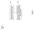
- FIG. 5 illustrates a more detailed view of T-shaped FPC 201 showing the traces for routing drive lines 101 and sense lines 103 of device 300 to an output of the FPC.
- the drive lines 101 and sense lines 103 are being routed to a connector pin 503 of, for example, a printed circuit board coupled to the output of T-shaped FPC 201 .
- the output of T-shaped FPC 201 can include exposed traces, connector pins, or any other appropriate coupling device.
- T-shaped FPC 201 can include two layers of traces with vias 501 for routing the traces between the layers. In FIG.
- the un-bolded solid lines represent traces located on the bottom layer of T-shaped FPC 201
- the dotted lines represent traces located on the top layer of T-shaped FPC 201
- the large dots represent vias 501 connecting the bottom layer to the top layer.
- T-shaped FPC 201 can include drive line traces 509 for routing drive lines 101 from first drive line contact portion 301 , drive line traces 511 for routing drive lines 101 from second drive line contact portion 303 , sense line traces 513 for routing sense lines 103 from first sense line contact portion 305 , and sense line traces 515 for routing sense lines 103 from second sense line contact portion 307 .
- T-shaped FPC 201 can include contact portions on the bottom side of the FPC to allow the traces 509 , 511 , 513 , and 515 to couple to the exposed segments of drive lines 101 and sense lines 103 at contact portions 301 , 303 , 305 , and 307 of device 300 .
- sense line traces 513 and 515 can be routed to connector pin 503 through the bottom layer and along the outer portion of the neck of T-shaped FPC 201 . Routing the sense line traces 513 and 515 in this way can leave open a channel at the crossbar portion of T-shaped FPC 201 (bottom of FIG. 5 ) through which the drive line traces 509 and 511 can couple together the drive lines 101 from first drive line contact portion 301 and second drive line contact portion 303 . Additionally, a channel can be left open at the center of T-shaped FPC 201 through which the coupled drive line traces 509 / 511 can be routed to connector pin 503 .
- a portion of the drive line traces 509 and 511 located at the outer ends of T-shaped FPC 201 (left and right sides of FIG. 5 ) can be routed towards the touch sensor panel 100 of device 300 (bottom of FIG. 5 ) where they can be routed up to the top layer of T-shaped FPC 201 through vias 501 .
- the outer drive line traces 509 and 511 can be routed together towards the center of T-shaped FPC 201 where all but one pair of drive line traces 509 and 511 can be coupled together by a second set of vias 501 .
- FIG. 5 In the embodiment shown in FIG.
- the vias 501 coupling together the outer drive line traces 509 and 511 can be arranged in a linear fashion.
- the vias 501 can be arranged in a staggered fashion, as illustrated by the vias 501 located at the left-middle portion of FIG. 5 .
- the combined outer drive line traces 509 / 511 from the second set of vias 501 can then be routed through the bottom layer at the center of T-shaped FPC 201 to connector pin 503 , while the remaining pair of drive line traces 509 and 511 can be coupled together near the second set of vias 501 and routed through the top layer at the center of T-shaped FPC 201 to connector pin 503 where they can be routed to the bottom layer through a via 501 and coupled to connector pin 503 .
- all but one pair of outer drive line traces 509 and 511 are shown as being coupled together by the second set of vias 501 , in some embodiments, all pairs of outer drive line traces 509 and 511 can be coupled together by vias 501 at the second set of vias 501 in a manner similar to that shown in FIG. 5 .
- the remaining drive line traces 509 and 511 located at the inner portion of T-shaped FPC 201 can be routed towards the touch sensor panel 100 of device 300 (bottom of FIG. 5 ). From there, the inner drive line traces 509 and 511 can be routed towards the center of T-shaped FPC 201 through the bottom layer where all but one pair of drive line traces 509 and 511 can be coupled together by a third set of vias 501 .
- the vias 501 coupling together the inner drive line traces 509 and 511 can be arranged in a staggered fashion.
- the vias 501 can be arranged in a linear fashion, as illustrated by the vias 501 located at the right-middle middle portion of FIG. 5 .
- the combined inner drive line traces 509 / 511 from the third set of vias 501 can then be routed through the top layer at the center of T-shaped FPC 201 towards connector pin 503 , where the combined inner drive line traces 509 / 511 can then be routed down to the bottom layer of T-shaped FPC 201 through another set of vias 501 .
- the remaining pair of drive line traces 509 and 511 can be coupled together near the third set of vias 501 and routed through the bottom layer at the center of T-shaped FPC 201 to couple to connector pin 503 .
- all but one pair of inner drive line traces 509 and 511 are shown as being coupled together by the third set of vias 501 , in some embodiments, all pairs of inner drive line traces 509 and 511 can be coupled together by vias 501 at the third set of vias 501 in a manner similar to that shown in FIG. 5 .
- drive lines 101 and sense lines 103 can be coupled to connector pin 503 using T-shaped FPC 201 without the traces for drive lines 101 and sense lines 103 intersecting or overlapping.
- drive line traces 509 and 511 may not cross paths with sense line traces 513 or 515 on the same or different layer of T-shaped FPC 201 . This can reduce or prevent the formation of unwanted parasitic capacitance between drive line traces 509 and 511 and sense line traces 513 or 515 that can result in false touch events and/or negative touch events due to the formation of additional pixels away from the active area of the panel 100 .
- drive line traces 509 or 511 may overlap with other drive line traces 509 or 511 , the formation of parasitic capacitance between drive line traces 509 or 511 may not result in the formation of additional pixels away from the active area of the panel 100 in the same way. Additionally, the ends of drive lines 101 can be coupled together by drive line traces 509 and 511 using relatively short trace lengths, thereby reducing the overall impedance of the drive lines 101 .
- T-shaped FPC 201 can further include guard traces 505 positioned between the drive line traces and sense line traces for reducing the capacitances between the sense line traces 513 and drive line traces 509 , and between sense line traces 515 and drive line traces 511 .
- guard traces 505 can be coupled to ground and can include a conductive material, such as silver or other metal.
- T-shaped FPC 201 was described above as having traces for eight drive lines 101 and six sense lines 103 , it should be appreciated that the configuration shown in FIG. 5 can be extended to any number of drive lines 101 and sense lines 103 .
- any number of sense line traces 513 and 515 can be routed along the outer edge of T-shaped FPC 201 to allow coupling between any number of drive line traces 509 and 511 and to allow the coupled drive line traces 509 / 511 to be routed through the center of the T-shaped FPC 201 to connector pin 503 .
- the outer drive line traces 509 and 511 can be coupled together on one of the layers (e.g., the top layer) of T-shaped FPC 201 , while the remaining inner drive line traces 509 and 511 can be coupled together on the other layer (e.g., the bottom layer) of T-shaped FPC 201 .
- the coupled inner and outer drive line traces 509 / 511 can then be routed to the opposite layer through a set of vias 501 arranged in either a staggered fashion or a linear fashion. From there, the drive lines 501 can be routed towards connector pin 503 where they can be routed to the bottom layer of T-shaped FPC 201 and coupled to the corresponding pins of connector pin 503 .
- FIG. 6 illustrates another embodiment of T-shaped FPC 201 in which one or more pairs (e.g., the outermost drive line traces 509 and 511 corresponding to the bottom drive line 101 row of panel 100 ) of drive line traces 509 and 511 may not be coupled together, thereby leaving a corresponding row of drive lines 101 uncoupled within T-shaped FPC 201 .
- This can be done to allow measurement of the impedance of the one or more uncoupled drive lines 101 for quality control purposes. For example, if the measured impedance is high, this can indicate that the touch response of touch sensor panel 100 may be poor, while a low impedance can indicate that an electrical short may be present in the device. While problems associated with other drive lines 101 may not be detected by measuring the impedance of the one or more uncoupled drive lines 101 , the one or more uncoupled drive lines 101 can provide a way to quickly compare touch sensor panels 100 that would not otherwise be available.
- the one or more uncoupled drive lines 101 can be coupled together in a location other than in the T-shaped FPC 201 .
- the ends of the one or more uncoupled drive lines 101 can be coupled together on a printed circuit board coupled to the output end of T-shaped FPC 201 .
- FIG. 7 shows another exemplary embodiment of device 300 in which T-shaped FPC 201 can be incorporated into the LCD FPC 705 .
- LCD FPC 705 can be coupled to the TFT glass 703 of device 300 and LCD backlight assembly 707 .
- LCD FPC 705 can include the already existing traces used for the LCD display, as well as the components of T-shaped FPC 201 with the exemplary trace routing described above.
- FIG. 8 shows an exemplary process 800 for routing rows of drive lines and columns of sense lines.
- a set of drive lines can be routed to an output using a first set of traces.
- the drive lines can be part of a touch sensor panel and can be operable to receive an AC stimulation signal for detecting touch events on the panel.
- the drive lines can be similar or identical to drive lines 101 of touch sensor panel 100 .
- the first set of traces can be included within a T-shaped FPC that is similar or identical to T-shaped FPC 201 .
- the ends of the drive lines can be coupled together by the first set of traces before reaching the output.
- the drive lines can be coupled together by a first set of traces that is similar or identical to drive line traces 509 and 511 .
- a set of sense lines can be routed to an output using a second set of traces.
- the sense lines can be part of a touch sensor panel and can intersect or overlap with the drive lines to form pixels within the touch sensor panel.
- the sense lines can further be operable to transmit touch or sense signals indicative of a touch event occurring on the panel.
- the sense lines can be similar or identical to sense lines 103 of touch sensor panel 100 .
- the second set of traces can be included within a T-shaped FPC that is similar or identical to T-shaped FPC 201 .
- the sense lines can be routed to the output without overlapping or intersecting with the first set of traces used to route the drive lines.
- the sense lines can be routed by a second set of traces that is similar or identical to sense line traces 513 and 515 .
- a T-shaped FPC as described above with respect to in FIGS. 2-8 can be incorporated into a mobile phone, a digital media player, a portable computer, touch pad, display device, PCB, and other suitable devices.
Abstract
Description
Claims (17)
Priority Applications (2)
| Application Number | Priority Date | Filing Date | Title |
|---|---|---|---|
| US14/204,427 US9201461B2 (en) | 2011-06-21 | 2014-03-11 | Flexible circuit routing of a touch sensitive display device comprising a set of drive lines and a set of sense lines |
| US14/952,664 US9600113B2 (en) | 2011-06-21 | 2015-11-25 | Touch sensitive display device comprising a flexible circuit routing having a set of drive lines and a set of sense lines wherein drive line traces and sense line traces are non-overlapping |
Applications Claiming Priority (2)
| Application Number | Priority Date | Filing Date | Title |
|---|---|---|---|
| US13/165,748 US8711570B2 (en) | 2011-06-21 | 2011-06-21 | Flexible circuit routing |
| US14/204,427 US9201461B2 (en) | 2011-06-21 | 2014-03-11 | Flexible circuit routing of a touch sensitive display device comprising a set of drive lines and a set of sense lines |
Related Parent Applications (1)
| Application Number | Title | Priority Date | Filing Date |
|---|---|---|---|
| US13/165,748 Division US8711570B2 (en) | 2011-06-21 | 2011-06-21 | Flexible circuit routing |
Related Child Applications (1)
| Application Number | Title | Priority Date | Filing Date |
|---|---|---|---|
| US14/952,664 Continuation US9600113B2 (en) | 2011-06-21 | 2015-11-25 | Touch sensitive display device comprising a flexible circuit routing having a set of drive lines and a set of sense lines wherein drive line traces and sense line traces are non-overlapping |
Publications (2)
| Publication Number | Publication Date |
|---|---|
| US20140192276A1 US20140192276A1 (en) | 2014-07-10 |
| US9201461B2 true US9201461B2 (en) | 2015-12-01 |
Family
ID=46545241
Family Applications (3)
| Application Number | Title | Priority Date | Filing Date |
|---|---|---|---|
| US13/165,748 Expired - Fee Related US8711570B2 (en) | 2011-06-21 | 2011-06-21 | Flexible circuit routing |
| US14/204,427 Expired - Fee Related US9201461B2 (en) | 2011-06-21 | 2014-03-11 | Flexible circuit routing of a touch sensitive display device comprising a set of drive lines and a set of sense lines |
| US14/952,664 Active US9600113B2 (en) | 2011-06-21 | 2015-11-25 | Touch sensitive display device comprising a flexible circuit routing having a set of drive lines and a set of sense lines wherein drive line traces and sense line traces are non-overlapping |
Family Applications Before (1)
| Application Number | Title | Priority Date | Filing Date |
|---|---|---|---|
| US13/165,748 Expired - Fee Related US8711570B2 (en) | 2011-06-21 | 2011-06-21 | Flexible circuit routing |
Family Applications After (1)
| Application Number | Title | Priority Date | Filing Date |
|---|---|---|---|
| US14/952,664 Active US9600113B2 (en) | 2011-06-21 | 2015-11-25 | Touch sensitive display device comprising a flexible circuit routing having a set of drive lines and a set of sense lines wherein drive line traces and sense line traces are non-overlapping |
Country Status (6)
| Country | Link |
|---|---|
| US (3) | US8711570B2 (en) |
| EP (1) | EP2538301A1 (en) |
| KR (1) | KR101563796B1 (en) |
| CN (1) | CN103765355B (en) |
| TW (1) | TWI462663B (en) |
| WO (1) | WO2012177351A1 (en) |
Cited By (6)
| Publication number | Priority date | Publication date | Assignee | Title |
|---|---|---|---|---|
| US20160077647A1 (en) * | 2011-06-21 | 2016-03-17 | Apple Inc. | Flexible circuit routing |
| US20170090650A1 (en) * | 2015-09-30 | 2017-03-30 | Samsung Display Co., Ltd. | Display device |
| US10216335B1 (en) * | 2016-10-18 | 2019-02-26 | Google Llc | Reducing false sensing of touchscreen inputs |
| US10680055B2 (en) | 2013-03-07 | 2020-06-09 | Semiconductor Energy Laboratory Co., Ltd. | Display device |
| US10990222B2 (en) | 2019-04-29 | 2021-04-27 | Google Llc | Calibration of trackpad |
| US11500489B2 (en) | 2019-01-30 | 2022-11-15 | Chengdu Boe Optoelectronics Technology Co., Ltd. | Flexible circuit board and manufacturing method, display device, circuit board structure and display panel thereof |
Families Citing this family (25)
| Publication number | Priority date | Publication date | Assignee | Title |
|---|---|---|---|---|
| KR20120137873A (en) * | 2011-06-13 | 2012-12-24 | 삼성전자주식회사 | Photographing appartus and electronic device |
| KR101871667B1 (en) * | 2012-03-16 | 2018-06-27 | 엘지디스플레이 주식회사 | Flexible printed circuit for connecting touch screen and liquid crystal display using the same |
| JP5819003B2 (en) * | 2012-09-27 | 2015-11-18 | シャープ株式会社 | Touch panel |
| TW201419061A (en) * | 2012-11-06 | 2014-05-16 | Wintek China Technology Ltd | Touch panel module and touch device therewith |
| US9618981B2 (en) | 2013-02-13 | 2017-04-11 | Synaptics Incorporated | Guarding and shielding routing traces in proximity sensors |
| TWI549025B (en) * | 2013-05-08 | 2016-09-11 | 廣達電腦股份有限公司 | Touch panel |
| TWI514228B (en) * | 2013-07-10 | 2015-12-21 | Innolux Corp | Display apparatus with touch sensor and method for manufacturing the same |
| US9658722B2 (en) * | 2013-09-26 | 2017-05-23 | Synaptics Incorporated | Using a printed circuit to offset charge during capacitive sensing |
| KR102181550B1 (en) | 2013-12-06 | 2020-11-23 | 삼성전자주식회사 | Electronic device having noise decrease means |
| CN103744564B (en) * | 2013-12-31 | 2016-08-17 | 深圳市华星光电技术有限公司 | A kind of single-layer capacitive touch module |
| TWM509378U (en) * | 2014-12-03 | 2015-09-21 | Futurelabs Entpr Co Ltd | Touch display device |
| US9535522B2 (en) * | 2014-12-22 | 2017-01-03 | Lg Display Co., Ltd. | Flexible organic light emitting diode display device |
| US10055040B2 (en) * | 2015-04-01 | 2018-08-21 | Shanghai Tianma Micro-electronics Co., Ltd. | Array substrate, touch display panel and touch display device |
| US10558309B2 (en) * | 2015-04-01 | 2020-02-11 | Shanghai Tianma Micro-electronics Co., Ltd. | Array substrate, touch display panel and touch display device |
| CN108541319B (en) * | 2015-11-20 | 2022-11-01 | 傲迪司威生物识别公司 | Electronic sensor supported on rigid substrate |
| US10120514B2 (en) * | 2016-06-24 | 2018-11-06 | Stmicroelectronics Asia Pacific Pte Ltd | Capacitive touch pressure sensor constructed from flexible substrate |
| KR102623575B1 (en) * | 2016-08-31 | 2024-01-11 | 엘지디스플레이 주식회사 | Driving chip, circuit film, chip on film typed driving circuit, and display device with a built-in touch screen |
| CN108803909A (en) * | 2017-04-27 | 2018-11-13 | 北京小米移动软件有限公司 | Display module, screen assembly and electronic equipment |
| WO2020156595A2 (en) * | 2019-01-30 | 2020-08-06 | 京东方科技集团股份有限公司 | Flexible circuit board and manufacturing method, display device, circuit board structure and display panel thereof |
| CN111511109B (en) | 2019-01-30 | 2021-11-23 | 京东方科技集团股份有限公司 | Flexible circuit board and manufacturing method thereof, electronic device module and electronic device |
| CN109976050B (en) * | 2019-04-15 | 2024-01-26 | 武汉华星光电技术有限公司 | Display panel and chip suitable for same |
| KR20210010733A (en) * | 2019-07-18 | 2021-01-28 | 삼성디스플레이 주식회사 | Display device |
| US11552344B2 (en) * | 2020-02-28 | 2023-01-10 | Gentherm Gmbh | Flex foil substrate connector for sensing battery voltage and temperature |
| KR20220152469A (en) * | 2021-05-07 | 2022-11-16 | 삼성디스플레이 주식회사 | Display device |
| JP7142755B1 (en) * | 2021-08-27 | 2022-09-27 | 株式会社ワコム | Position detector and sensor panel |
Citations (89)
| Publication number | Priority date | Publication date | Assignee | Title |
|---|---|---|---|---|
| US4116517A (en) | 1976-04-15 | 1978-09-26 | International Telephone And Telegraph Corporation | Flexible printed circuit and electrical connection therefor |
| US4687695A (en) | 1985-09-27 | 1987-08-18 | Hamby Bill L | Flexible printed circuits and methods of fabricating and forming plated thru-holes therein |
| US5483261A (en) | 1992-02-14 | 1996-01-09 | Itu Research, Inc. | Graphical input controller and method with rear screen image detection |
| US5488204A (en) | 1992-06-08 | 1996-01-30 | Synaptics, Incorporated | Paintbrush stylus for capacitive touch sensor pad |
| US5670994A (en) | 1993-01-27 | 1997-09-23 | Sharp Kabushiki Kaisha | Assembly structure of a flat type device including a panel having electrode terminals disposed on a peripheral portion |
| US5737053A (en) | 1995-06-05 | 1998-04-07 | Kabushiki Kaisha Toshiba | Wire substrate having branch lines perpendicular to the main lines in which the branch lines connect to driving circuits on a display device |
| US5771158A (en) | 1995-09-21 | 1998-06-23 | Mitsubishi Denki Kabushiki Kaisha | Printed circuit board, printed circuit board used for flat panel display drive circuit, and flat panel display device |
| US5825352A (en) | 1996-01-04 | 1998-10-20 | Logitech, Inc. | Multiple fingers contact sensing method for emulating mouse buttons and mouse operations on a touch sensor pad |
| US5835079A (en) | 1996-06-13 | 1998-11-10 | International Business Machines Corporation | Virtual pointing device for touchscreens |
| US5880411A (en) | 1992-06-08 | 1999-03-09 | Synaptics, Incorporated | Object position detector with edge motion feature and gesture recognition |
| US5920309A (en) | 1996-01-04 | 1999-07-06 | Logitech, Inc. | Touch sensing method and apparatus |
| US6061246A (en) | 1997-09-13 | 2000-05-09 | Samsung Electronics Co., Ltd. | Microelectric packages including flexible layers and flexible extensions, and liquid crystal display modules using the same |
| JP2000163031A (en) | 1998-11-25 | 2000-06-16 | Seiko Epson Corp | Portable information equipment and information storage medium |
| US6157541A (en) | 1997-12-30 | 2000-12-05 | Siemens Aktiengesellschaft | Stack arrangement for two semiconductor memory chips and printed board for accepting a plurality of such stack arrangements |
| US6188391B1 (en) | 1998-07-09 | 2001-02-13 | Synaptics, Inc. | Two-layer capacitive touchpad and method of making same |
| US6310610B1 (en) | 1997-12-04 | 2001-10-30 | Nortel Networks Limited | Intelligent touch display |
| US6323846B1 (en) | 1998-01-26 | 2001-11-27 | University Of Delaware | Method and apparatus for integrating manual input |
| US6471415B1 (en) | 2000-07-18 | 2002-10-29 | Hewlett-Packard Company | Multiconductor interconnect |
| US20020167494A1 (en) | 2001-02-15 | 2002-11-14 | Sherman Nathan C. | Keyboard key discrimination employing drive line/sense line combinations and accomodating simultaneous key press conditions |
| JP2002342033A (en) | 2001-05-21 | 2002-11-29 | Sony Corp | Non-contact type user input device |
| US6519021B1 (en) | 1999-01-18 | 2003-02-11 | Seiko Epson Corporation | Wiring board for connection of electro-optical panel, electro-optical device and electronic apparatus |
| US6690387B2 (en) | 2001-12-28 | 2004-02-10 | Koninklijke Philips Electronics N.V. | Touch-screen image scrolling system and method |
| US20050040504A1 (en) | 2003-08-05 | 2005-02-24 | Sa-Yoon Kang | Low-cost flexible film package module and method of manufacturing the same |
| US6870590B2 (en) | 2000-08-10 | 2005-03-22 | Seiko Epson Corporation | Electrooptical unit with a flexible board and electronic apparatus |
| US6952870B2 (en) | 2001-07-31 | 2005-10-11 | Koninklijke Philips Electronics | Integrated circuit wiring method |
| US7015894B2 (en) | 2001-09-28 | 2006-03-21 | Ricoh Company, Ltd. | Information input and output system, method, storage medium, and carrier wave |
| US7095476B2 (en) | 2004-10-15 | 2006-08-22 | Wintek Corporation | Liquid crystal module |
| US20060197753A1 (en) | 2005-03-04 | 2006-09-07 | Hotelling Steven P | Multi-functional hand-held device |
| US7119801B1 (en) | 1999-03-26 | 2006-10-10 | Seiko Epson Corporation | Display device and electronic apparatus |
| US20060256099A1 (en) | 2005-05-16 | 2006-11-16 | Mitsubishi Denki Kabushiki Kaisha | Display and timing controller |
| US20070035473A1 (en) | 2005-08-12 | 2007-02-15 | Semiconductor Energy Laboratory Co., Ltd. | Display module, and cellular phone and electronic device provided with display module |
| WO2007146785A2 (en) | 2006-06-09 | 2007-12-21 | Apple Inc. | Touch screen liquid crystal display |
| US20080006453A1 (en) | 2006-07-06 | 2008-01-10 | Apple Computer, Inc., A California Corporation | Mutual capacitance touch sensing device |
| US20080018849A1 (en) | 2006-07-11 | 2008-01-24 | Toshiba Matsushita Display Technology Co., Ltd. | Display element |
| US7349054B2 (en) | 2001-11-22 | 2008-03-25 | Advanced Display, Inc. | Method of mounting flexible circuit boards, and display device |
| US20080074398A1 (en) | 2006-09-26 | 2008-03-27 | David Gordon Wright | Single-layer capacitive sensing device |
| US20080074853A1 (en) | 2006-09-22 | 2008-03-27 | Jang Jin-Seok | Flexible printed circuit board |
| US20080158181A1 (en) | 2007-01-03 | 2008-07-03 | Apple Computer, Inc. | Double-sided touch sensitive panel and flex circuit bonding |
| US20080158167A1 (en) | 2007-01-03 | 2008-07-03 | Apple Computer, Inc. | Simultaneous sensing arrangement |
| US20080158183A1 (en) | 2007-01-03 | 2008-07-03 | Apple Computer, Inc. | Double-sided touch-sensitive panel with shield and drive combined layer |
| US20080164056A1 (en) | 2007-01-05 | 2008-07-10 | Apple Computer, Inc. | Compact display flex and driver sub-assemblies |
| US20080232047A1 (en) | 2007-03-19 | 2008-09-25 | Epson Imaging Devices Corporation | Mounting structure, electro-optical device, input device, method of manufacturing mounting structure, and electronic apparatus |
| US7432451B2 (en) | 2005-01-24 | 2008-10-07 | Seiko Epson Corporation | Electro-optical device, circuit board, mounting structure, and electronic apparatus |
| US20080309633A1 (en) | 2007-06-13 | 2008-12-18 | Apple Inc. | Touch-sensitive display |
| US7518691B2 (en) | 2004-07-13 | 2009-04-14 | Seiko Epson Corporation | Electrooptical device, mounting structure, and electronic apparatus having wiring formed on and protruding from a base material to directly under an input bump on a semiconductor device |
| US20090135364A1 (en) | 2007-11-28 | 2009-05-28 | Samsung Electronics Co., Ltd. | Single-sided printed circuit board and liquid crystal display having the same |
| US20090207336A1 (en) | 2008-02-18 | 2009-08-20 | Lee Jung-Sun | Flexible printed circuit board and display device having the same |
| US20090266621A1 (en) | 2008-04-25 | 2009-10-29 | Apple Inc. | Reliability Metal Traces |
| US20090273570A1 (en) | 2008-04-30 | 2009-11-05 | Apple Inc. | Multi-touch sensor patterns and stack-ups |
| US20090283300A1 (en) | 2008-05-16 | 2009-11-19 | Apple Inc. | Flex Circuit with Single Sided Routing and Double Sided Attach |
| US20090303189A1 (en) | 2008-06-06 | 2009-12-10 | Grunthaner Martin Paul | High Resistivity Metal Fan Out |
| US20090314621A1 (en) | 2008-04-25 | 2009-12-24 | Apple Inc. | Brick Layout and Stackup for a Touch Screen |
| US7663607B2 (en) | 2004-05-06 | 2010-02-16 | Apple Inc. | Multipoint touchscreen |
| US20100059294A1 (en) | 2008-09-08 | 2010-03-11 | Apple Inc. | Bandwidth enhancement for a touch sensor panel |
| US20100079387A1 (en) | 2008-09-30 | 2010-04-01 | Michael Nathaniel Rosenblatt | Integrated touch sensor and solar assembly |
| US20100085326A1 (en) | 2008-10-03 | 2010-04-08 | Hitachi Displays, Ltd. | Display device |
| US20100110040A1 (en) | 2008-10-30 | 2010-05-06 | Samsung Electronics Co., Ltd. | Touch controller having increased sensing sensitivity, and display driving circuit and display device and system having the touch controller |
| US20100149108A1 (en) | 2008-12-11 | 2010-06-17 | Steve Porter Hotelling | Single layer touch panel with segmented drive and sense electrodes |
| US20100315399A1 (en) | 2009-06-10 | 2010-12-16 | Jacobson Joseph M | Flexible Electronic Device and Method of Manufacture |
| US20100321326A1 (en) | 2009-06-19 | 2010-12-23 | Grunthaner Martin Paul | Direct Connect Single Layer Touch Panel |
| US20110001706A1 (en) | 2009-07-02 | 2011-01-06 | Emery Sanford | Electronic device touch screen display module |
| US20110012845A1 (en) | 2009-07-20 | 2011-01-20 | Rothkopf Fletcher R | Touch sensor structures for displays |
| US20110025660A1 (en) | 2009-07-30 | 2011-02-03 | Yoojin Song | Plasma display device |
| US20110050617A1 (en) | 2009-08-25 | 2011-03-03 | Avago Technologies Ecbu (Singapore) Pte. Ltd. | Method and Apparatus for Detecting Defective Traces in a Mutual Capacitance Touch Sensing Device |
| US20110074705A1 (en) | 2009-09-30 | 2011-03-31 | Marduke Yousefpor | Touch Screen Border Regions |
| KR20110042585A (en) | 2009-10-19 | 2011-04-27 | 삼성전자주식회사 | Touch controller increasing sensitivity, display driving circuit and display device and system having the same |
| US20110102729A1 (en) | 2008-07-08 | 2011-05-05 | Sharp Kabushiki Kaisha | Flexible printed circuit and electric circuit structure |
| US20110134075A1 (en) | 2008-08-07 | 2011-06-09 | Sharp Kabushiki Kaisha | Touch panel, display, and electronic device |
| US7965367B2 (en) | 2008-02-15 | 2011-06-21 | Hitachi Displays, Ltd. | Display device having flexible printed circuit board with particular differential signal lines connection |
| US20110199738A1 (en) | 2008-12-05 | 2011-08-18 | Hiroyuki Moriwaki | Substrate for display device and display device |
| US8031150B2 (en) | 1999-04-16 | 2011-10-04 | Samsung Electronics Co., Ltd. | Liquid crystal display panel with signal transmission patterns |
| US20110254830A1 (en) | 2010-04-20 | 2011-10-20 | Chia-Hsien Chang | Scan signal transmission system and method thereof |
| US20110254758A1 (en) | 2010-04-19 | 2011-10-20 | Qualcomm Mems Technologies, Inc. | Flex Design and Attach Method for Reducing Display Panel Periphery |
| US20110267562A1 (en) * | 2009-04-17 | 2011-11-03 | Yuji Yashiro | Liquid crystal panel |
| US20110279400A1 (en) | 2010-05-14 | 2011-11-17 | Atmel Corporation | Panel for position sensors |
| US20110285640A1 (en) * | 2010-05-21 | 2011-11-24 | Park Young-Bae | Electric field shielding for in-cell touch type thin-film-transistor liquid crystal displays |
| US20110310054A1 (en) | 2010-06-21 | 2011-12-22 | Avago Technologies Ecbu Ip (Singapore) Pte. Ltd. | Capacitive Touchscreen Signal Acquisition without Panel Reset |
| US20120057312A1 (en) | 2010-09-07 | 2012-03-08 | Young-Seok Yoo | Flexible printed circuit board and touch screen panel apparatus having the same |
| US20120162090A1 (en) | 2010-12-22 | 2012-06-28 | Shih Chang Chang | Relay driving of displays |
| US20120162584A1 (en) | 2010-12-22 | 2012-06-28 | Shih Chang Chang | Integrated touch screens |
| US8217913B2 (en) | 2009-02-02 | 2012-07-10 | Apple Inc. | Integrated touch screen |
| US8217924B2 (en) | 2007-12-28 | 2012-07-10 | Samsung Electronics Co., Ltd. | Display apparatus and method of driving the same |
| WO2012177351A1 (en) | 2011-06-21 | 2012-12-27 | Apple Inc. | Flexible circuit routing |
| US20130044443A1 (en) | 2011-08-17 | 2013-02-21 | Fujitsu Component Limited | Flexible printed circuit and touchscreen |
| US20130141912A1 (en) | 2011-12-06 | 2013-06-06 | Hun Tae KIM | Circuit board for display device and display device having the same |
| USRE44314E1 (en) | 1998-12-02 | 2013-06-25 | Hitachi Displays, Ltd. | Liquid crystal display device |
| US8479122B2 (en) | 2004-07-30 | 2013-07-02 | Apple Inc. | Gestures for touch sensitive input devices |
| US20130201620A1 (en) | 2012-02-06 | 2013-08-08 | Alexander D. Schlaupitz | Flexible Circuit Connectors with Reduced Profiles |
| US8564550B2 (en) | 2008-08-06 | 2013-10-22 | Hitachi Displays, Ltd. | Display device with X and Y electrodes having both ends of a respective electrode supplied with a signal form a branched signal line |
Family Cites Families (3)
| Publication number | Priority date | Publication date | Assignee | Title |
|---|---|---|---|---|
| KR100898930B1 (en) * | 2007-09-04 | 2009-05-26 | 엘지전자 주식회사 | Temperature and humidity controlling apparatus of dryer |
| US8563983B2 (en) * | 2009-08-25 | 2013-10-22 | Sharp Kabushiki Kaisha | Display panel, display device, and method manufacturing same |
| US20130265282A1 (en) * | 2010-12-08 | 2013-10-10 | Sharp Kabushiki Kaisha | Touch panel and display device with touch panel |
-
2011
- 2011-06-21 US US13/165,748 patent/US8711570B2/en not_active Expired - Fee Related
-
2012
- 2012-05-23 CN CN201280028060.3A patent/CN103765355B/en active Active
- 2012-05-23 WO PCT/US2012/039072 patent/WO2012177351A1/en active Application Filing
- 2012-05-23 KR KR1020137031189A patent/KR101563796B1/en active IP Right Grant
- 2012-05-31 EP EP12170190A patent/EP2538301A1/en not_active Withdrawn
- 2012-06-18 TW TW101121800A patent/TWI462663B/en not_active IP Right Cessation
-
2014
- 2014-03-11 US US14/204,427 patent/US9201461B2/en not_active Expired - Fee Related
-
2015
- 2015-11-25 US US14/952,664 patent/US9600113B2/en active Active
Patent Citations (99)
| Publication number | Priority date | Publication date | Assignee | Title |
|---|---|---|---|---|
| US4116517A (en) | 1976-04-15 | 1978-09-26 | International Telephone And Telegraph Corporation | Flexible printed circuit and electrical connection therefor |
| US4687695A (en) | 1985-09-27 | 1987-08-18 | Hamby Bill L | Flexible printed circuits and methods of fabricating and forming plated thru-holes therein |
| US5483261A (en) | 1992-02-14 | 1996-01-09 | Itu Research, Inc. | Graphical input controller and method with rear screen image detection |
| US5488204A (en) | 1992-06-08 | 1996-01-30 | Synaptics, Incorporated | Paintbrush stylus for capacitive touch sensor pad |
| US5880411A (en) | 1992-06-08 | 1999-03-09 | Synaptics, Incorporated | Object position detector with edge motion feature and gesture recognition |
| US5670994A (en) | 1993-01-27 | 1997-09-23 | Sharp Kabushiki Kaisha | Assembly structure of a flat type device including a panel having electrode terminals disposed on a peripheral portion |
| US5737053A (en) | 1995-06-05 | 1998-04-07 | Kabushiki Kaisha Toshiba | Wire substrate having branch lines perpendicular to the main lines in which the branch lines connect to driving circuits on a display device |
| US5771158A (en) | 1995-09-21 | 1998-06-23 | Mitsubishi Denki Kabushiki Kaisha | Printed circuit board, printed circuit board used for flat panel display drive circuit, and flat panel display device |
| US5825352A (en) | 1996-01-04 | 1998-10-20 | Logitech, Inc. | Multiple fingers contact sensing method for emulating mouse buttons and mouse operations on a touch sensor pad |
| US5920309A (en) | 1996-01-04 | 1999-07-06 | Logitech, Inc. | Touch sensing method and apparatus |
| US5835079A (en) | 1996-06-13 | 1998-11-10 | International Business Machines Corporation | Virtual pointing device for touchscreens |
| US6061246A (en) | 1997-09-13 | 2000-05-09 | Samsung Electronics Co., Ltd. | Microelectric packages including flexible layers and flexible extensions, and liquid crystal display modules using the same |
| US6310610B1 (en) | 1997-12-04 | 2001-10-30 | Nortel Networks Limited | Intelligent touch display |
| US6157541A (en) | 1997-12-30 | 2000-12-05 | Siemens Aktiengesellschaft | Stack arrangement for two semiconductor memory chips and printed board for accepting a plurality of such stack arrangements |
| US6323846B1 (en) | 1998-01-26 | 2001-11-27 | University Of Delaware | Method and apparatus for integrating manual input |
| US6188391B1 (en) | 1998-07-09 | 2001-02-13 | Synaptics, Inc. | Two-layer capacitive touchpad and method of making same |
| JP2000163031A (en) | 1998-11-25 | 2000-06-16 | Seiko Epson Corp | Portable information equipment and information storage medium |
| USRE44314E1 (en) | 1998-12-02 | 2013-06-25 | Hitachi Displays, Ltd. | Liquid crystal display device |
| US6519021B1 (en) | 1999-01-18 | 2003-02-11 | Seiko Epson Corporation | Wiring board for connection of electro-optical panel, electro-optical device and electronic apparatus |
| US7119801B1 (en) | 1999-03-26 | 2006-10-10 | Seiko Epson Corporation | Display device and electronic apparatus |
| US8031150B2 (en) | 1999-04-16 | 2011-10-04 | Samsung Electronics Co., Ltd. | Liquid crystal display panel with signal transmission patterns |
| US6471415B1 (en) | 2000-07-18 | 2002-10-29 | Hewlett-Packard Company | Multiconductor interconnect |
| US6870590B2 (en) | 2000-08-10 | 2005-03-22 | Seiko Epson Corporation | Electrooptical unit with a flexible board and electronic apparatus |
| US20020167494A1 (en) | 2001-02-15 | 2002-11-14 | Sherman Nathan C. | Keyboard key discrimination employing drive line/sense line combinations and accomodating simultaneous key press conditions |
| JP2002342033A (en) | 2001-05-21 | 2002-11-29 | Sony Corp | Non-contact type user input device |
| US7715204B2 (en) | 2001-07-31 | 2010-05-11 | Koninklijke Philips Electronics N.V. | Ultrasound probe wiring apparatus |
| US6952870B2 (en) | 2001-07-31 | 2005-10-11 | Koninklijke Philips Electronics | Integrated circuit wiring method |
| US7015894B2 (en) | 2001-09-28 | 2006-03-21 | Ricoh Company, Ltd. | Information input and output system, method, storage medium, and carrier wave |
| US7349054B2 (en) | 2001-11-22 | 2008-03-25 | Advanced Display, Inc. | Method of mounting flexible circuit boards, and display device |
| US6690387B2 (en) | 2001-12-28 | 2004-02-10 | Koninklijke Philips Electronics N.V. | Touch-screen image scrolling system and method |
| US7184064B2 (en) | 2001-12-28 | 2007-02-27 | Koninklijke Philips Electronics N.V. | Touch-screen image scrolling system and method |
| US20050040504A1 (en) | 2003-08-05 | 2005-02-24 | Sa-Yoon Kang | Low-cost flexible film package module and method of manufacturing the same |
| US20060268213A1 (en) | 2003-08-05 | 2006-11-30 | Sa-Yoon Kang | Low-cost flexible film package module and method of manufacturing the same |
| US7663607B2 (en) | 2004-05-06 | 2010-02-16 | Apple Inc. | Multipoint touchscreen |
| US7518691B2 (en) | 2004-07-13 | 2009-04-14 | Seiko Epson Corporation | Electrooptical device, mounting structure, and electronic apparatus having wiring formed on and protruding from a base material to directly under an input bump on a semiconductor device |
| US8479122B2 (en) | 2004-07-30 | 2013-07-02 | Apple Inc. | Gestures for touch sensitive input devices |
| US7095476B2 (en) | 2004-10-15 | 2006-08-22 | Wintek Corporation | Liquid crystal module |
| US7432451B2 (en) | 2005-01-24 | 2008-10-07 | Seiko Epson Corporation | Electro-optical device, circuit board, mounting structure, and electronic apparatus |
| US20060197753A1 (en) | 2005-03-04 | 2006-09-07 | Hotelling Steven P | Multi-functional hand-held device |
| US20060256099A1 (en) | 2005-05-16 | 2006-11-16 | Mitsubishi Denki Kabushiki Kaisha | Display and timing controller |
| US20070035473A1 (en) | 2005-08-12 | 2007-02-15 | Semiconductor Energy Laboratory Co., Ltd. | Display module, and cellular phone and electronic device provided with display module |
| WO2007146785A2 (en) | 2006-06-09 | 2007-12-21 | Apple Inc. | Touch screen liquid crystal display |
| US20080006453A1 (en) | 2006-07-06 | 2008-01-10 | Apple Computer, Inc., A California Corporation | Mutual capacitance touch sensing device |
| US20080018849A1 (en) | 2006-07-11 | 2008-01-24 | Toshiba Matsushita Display Technology Co., Ltd. | Display element |
| US20080074853A1 (en) | 2006-09-22 | 2008-03-27 | Jang Jin-Seok | Flexible printed circuit board |
| US20080074398A1 (en) | 2006-09-26 | 2008-03-27 | David Gordon Wright | Single-layer capacitive sensing device |
| US20080158183A1 (en) | 2007-01-03 | 2008-07-03 | Apple Computer, Inc. | Double-sided touch-sensitive panel with shield and drive combined layer |
| TW200843220A (en) | 2007-01-03 | 2008-11-01 | Apple Inc | Double-sided touch-sensitive panel and flex circuit bonding |
| US20080158167A1 (en) | 2007-01-03 | 2008-07-03 | Apple Computer, Inc. | Simultaneous sensing arrangement |
| US8026903B2 (en) | 2007-01-03 | 2011-09-27 | Apple Inc. | Double-sided touch sensitive panel and flex circuit bonding |
| US20110094993A1 (en) | 2007-01-03 | 2011-04-28 | Mark Arthur Hamblin | Double-sided touch sensitive panel and flex circuit bonding |
| US20080158181A1 (en) | 2007-01-03 | 2008-07-03 | Apple Computer, Inc. | Double-sided touch sensitive panel and flex circuit bonding |
| US20080164056A1 (en) | 2007-01-05 | 2008-07-10 | Apple Computer, Inc. | Compact display flex and driver sub-assemblies |
| US20080232047A1 (en) | 2007-03-19 | 2008-09-25 | Epson Imaging Devices Corporation | Mounting structure, electro-optical device, input device, method of manufacturing mounting structure, and electronic apparatus |
| US20080309633A1 (en) | 2007-06-13 | 2008-12-18 | Apple Inc. | Touch-sensitive display |
| US20090135364A1 (en) | 2007-11-28 | 2009-05-28 | Samsung Electronics Co., Ltd. | Single-sided printed circuit board and liquid crystal display having the same |
| US8217924B2 (en) | 2007-12-28 | 2012-07-10 | Samsung Electronics Co., Ltd. | Display apparatus and method of driving the same |
| US7965367B2 (en) | 2008-02-15 | 2011-06-21 | Hitachi Displays, Ltd. | Display device having flexible printed circuit board with particular differential signal lines connection |
| US20090207336A1 (en) | 2008-02-18 | 2009-08-20 | Lee Jung-Sun | Flexible printed circuit board and display device having the same |
| US20090266621A1 (en) | 2008-04-25 | 2009-10-29 | Apple Inc. | Reliability Metal Traces |
| US20090314621A1 (en) | 2008-04-25 | 2009-12-24 | Apple Inc. | Brick Layout and Stackup for a Touch Screen |
| US20090273570A1 (en) | 2008-04-30 | 2009-11-05 | Apple Inc. | Multi-touch sensor patterns and stack-ups |
| US20090283300A1 (en) | 2008-05-16 | 2009-11-19 | Apple Inc. | Flex Circuit with Single Sided Routing and Double Sided Attach |
| US20090303189A1 (en) | 2008-06-06 | 2009-12-10 | Grunthaner Martin Paul | High Resistivity Metal Fan Out |
| US20110102729A1 (en) | 2008-07-08 | 2011-05-05 | Sharp Kabushiki Kaisha | Flexible printed circuit and electric circuit structure |
| US8564550B2 (en) | 2008-08-06 | 2013-10-22 | Hitachi Displays, Ltd. | Display device with X and Y electrodes having both ends of a respective electrode supplied with a signal form a branched signal line |
| US20110134075A1 (en) | 2008-08-07 | 2011-06-09 | Sharp Kabushiki Kaisha | Touch panel, display, and electronic device |
| US20100059294A1 (en) | 2008-09-08 | 2010-03-11 | Apple Inc. | Bandwidth enhancement for a touch sensor panel |
| US20100079387A1 (en) | 2008-09-30 | 2010-04-01 | Michael Nathaniel Rosenblatt | Integrated touch sensor and solar assembly |
| US8493345B2 (en) | 2008-10-03 | 2013-07-23 | Hitachi Displays, Ltd. | Display device |
| US20100085326A1 (en) | 2008-10-03 | 2010-04-08 | Hitachi Displays, Ltd. | Display device |
| TW201023129A (en) | 2008-10-30 | 2010-06-16 | Samsung Electronics Co Ltd | Touch controller having increased sensing sensitivity, and display driving circuit and display device and system having the touch controller |
| US20100110040A1 (en) | 2008-10-30 | 2010-05-06 | Samsung Electronics Co., Ltd. | Touch controller having increased sensing sensitivity, and display driving circuit and display device and system having the touch controller |
| US20110199738A1 (en) | 2008-12-05 | 2011-08-18 | Hiroyuki Moriwaki | Substrate for display device and display device |
| US20100149108A1 (en) | 2008-12-11 | 2010-06-17 | Steve Porter Hotelling | Single layer touch panel with segmented drive and sense electrodes |
| US8217913B2 (en) | 2009-02-02 | 2012-07-10 | Apple Inc. | Integrated touch screen |
| US20110267562A1 (en) * | 2009-04-17 | 2011-11-03 | Yuji Yashiro | Liquid crystal panel |
| US20100315399A1 (en) | 2009-06-10 | 2010-12-16 | Jacobson Joseph M | Flexible Electronic Device and Method of Manufacture |
| US20100321326A1 (en) | 2009-06-19 | 2010-12-23 | Grunthaner Martin Paul | Direct Connect Single Layer Touch Panel |
| US20110001706A1 (en) | 2009-07-02 | 2011-01-06 | Emery Sanford | Electronic device touch screen display module |
| US20110012845A1 (en) | 2009-07-20 | 2011-01-20 | Rothkopf Fletcher R | Touch sensor structures for displays |
| US20110025660A1 (en) | 2009-07-30 | 2011-02-03 | Yoojin Song | Plasma display device |
| US20110050617A1 (en) | 2009-08-25 | 2011-03-03 | Avago Technologies Ecbu (Singapore) Pte. Ltd. | Method and Apparatus for Detecting Defective Traces in a Mutual Capacitance Touch Sensing Device |
| US20110074705A1 (en) | 2009-09-30 | 2011-03-31 | Marduke Yousefpor | Touch Screen Border Regions |
| KR20110042585A (en) | 2009-10-19 | 2011-04-27 | 삼성전자주식회사 | Touch controller increasing sensitivity, display driving circuit and display device and system having the same |
| US20110254758A1 (en) | 2010-04-19 | 2011-10-20 | Qualcomm Mems Technologies, Inc. | Flex Design and Attach Method for Reducing Display Panel Periphery |
| US20110254830A1 (en) | 2010-04-20 | 2011-10-20 | Chia-Hsien Chang | Scan signal transmission system and method thereof |
| US20110279400A1 (en) | 2010-05-14 | 2011-11-17 | Atmel Corporation | Panel for position sensors |
| US20110285640A1 (en) * | 2010-05-21 | 2011-11-24 | Park Young-Bae | Electric field shielding for in-cell touch type thin-film-transistor liquid crystal displays |
| US20110310054A1 (en) | 2010-06-21 | 2011-12-22 | Avago Technologies Ecbu Ip (Singapore) Pte. Ltd. | Capacitive Touchscreen Signal Acquisition without Panel Reset |
| US20120057312A1 (en) | 2010-09-07 | 2012-03-08 | Young-Seok Yoo | Flexible printed circuit board and touch screen panel apparatus having the same |
| US20120162090A1 (en) | 2010-12-22 | 2012-06-28 | Shih Chang Chang | Relay driving of displays |
| US20120162584A1 (en) | 2010-12-22 | 2012-06-28 | Shih Chang Chang | Integrated touch screens |
| US20120326990A1 (en) | 2011-06-21 | 2012-12-27 | Wurzel Joshua G | Flexible circuit routing |
| WO2012177351A1 (en) | 2011-06-21 | 2012-12-27 | Apple Inc. | Flexible circuit routing |
| US8711570B2 (en) | 2011-06-21 | 2014-04-29 | Apple Inc. | Flexible circuit routing |
| US20130044443A1 (en) | 2011-08-17 | 2013-02-21 | Fujitsu Component Limited | Flexible printed circuit and touchscreen |
| US20130141912A1 (en) | 2011-12-06 | 2013-06-06 | Hun Tae KIM | Circuit board for display device and display device having the same |
| US20130201620A1 (en) | 2012-02-06 | 2013-08-08 | Alexander D. Schlaupitz | Flexible Circuit Connectors with Reduced Profiles |
Non-Patent Citations (10)
| Title |
|---|
| European Search Report mailed Oct. 26, 2012, for EP Appliction No. 12170190.8, seven pages. |
| International Search Report mailed Aug. 31, 2012, for PCT Application No. PCT/US12/39072, filed May 23, 2012, three pages. |
| Lee, S.K. et al. (Apr. 1985). "A Multi-Touch Three Dimensional Touch-Sensitive Tablet," Proceedings of CHI: ACM Conference on Human Factors in Computing Systems, pp. 21-25. |
| Non-Final Office Action mailed Jul. 30, 2013; for U.S. Appl. No. 13/165,748, filed Jun. 21, 2011, thirteen pages. |
| Notice of Allowance mailed Dec. 20, 2013; for U.S. Appl. No. 13/165,748, filed Jun. 21, 2011, ten pages. |
| Rubine, D.H. (Dec. 1991). "The Automatic Recognition of Gestures," CMU-CS-91-202, Submitted in Partial Fulfillment of the Requirements for the Degree of Doctor of Philosophy in Computer Science at Carnegie Mellon University, 285 pages. |
| Rubine, D.H. (May 1992). "Combining Gestures and Direct Manipulation," CHI '92, pp. 659-660. |
| Schoening, J. et al. (Oct. 2008). "Multi-Touch Surfaces: A Technical Guide," Technical Report TUM-10833, Technical Reports of the Technical University of Munich, located at http://ar.in.tum.de/pub/schoening2008multitouch/schoening2008multitouch.pdf, last visited Aug. 9, 2012, 19 pages. |
| Schoening, J. et al. (Oct. 2008). "Multi-Touch Surfaces: A Technical Guide," Technical Report TUM-10833, Technical Reports of the Technical University of Munich, located at http://www.citeulike.org/group/7653/article/3431399, last visited Aug. 11, 2012, one page. |
| Westerman, W. (Spring 1999). "Hand Tracking, Finger Identification, and Chordic Manipulation on a Multi-Touch Surface," A Dissertation Submitted to the Faculty of the University of Delaware in Partial Fulfillment of the Requirements for the Degree of Doctor of Philosophy in Electrical Engineering, 364 pages. |
Cited By (11)
| Publication number | Priority date | Publication date | Assignee | Title |
|---|---|---|---|---|
| US20160077647A1 (en) * | 2011-06-21 | 2016-03-17 | Apple Inc. | Flexible circuit routing |
| US9600113B2 (en) * | 2011-06-21 | 2017-03-21 | Apple Inc. | Touch sensitive display device comprising a flexible circuit routing having a set of drive lines and a set of sense lines wherein drive line traces and sense line traces are non-overlapping |
| US10680055B2 (en) | 2013-03-07 | 2020-06-09 | Semiconductor Energy Laboratory Co., Ltd. | Display device |
| US11271070B2 (en) | 2013-03-07 | 2022-03-08 | Semiconductor Energy Laboratory Co., Ltd. | Display device |
| US11678538B2 (en) | 2013-03-07 | 2023-06-13 | Semiconductor Energy Laboratory Co., Ltd. | Display device |
| US11950474B2 (en) | 2013-03-07 | 2024-04-02 | Semiconductor Energy Laboratory Co., Ltd. | Display device |
| US20170090650A1 (en) * | 2015-09-30 | 2017-03-30 | Samsung Display Co., Ltd. | Display device |
| US10216335B1 (en) * | 2016-10-18 | 2019-02-26 | Google Llc | Reducing false sensing of touchscreen inputs |
| US11500489B2 (en) | 2019-01-30 | 2022-11-15 | Chengdu Boe Optoelectronics Technology Co., Ltd. | Flexible circuit board and manufacturing method, display device, circuit board structure and display panel thereof |
| US11934606B2 (en) | 2019-01-30 | 2024-03-19 | Chengdu Boe Optoelectronics Technology Co., Ltd. | Flexible circuit board and manufacturing method, display device, circuit board structure and display panel thereof |
| US10990222B2 (en) | 2019-04-29 | 2021-04-27 | Google Llc | Calibration of trackpad |
Also Published As
| Publication number | Publication date |
|---|---|
| US9600113B2 (en) | 2017-03-21 |
| CN103765355A (en) | 2014-04-30 |
| US8711570B2 (en) | 2014-04-29 |
| US20160077647A1 (en) | 2016-03-17 |
| US20120326990A1 (en) | 2012-12-27 |
| TWI462663B (en) | 2014-11-21 |
| EP2538301A1 (en) | 2012-12-26 |
| US20140192276A1 (en) | 2014-07-10 |
| TW201309130A (en) | 2013-02-16 |
| CN103765355B (en) | 2016-10-12 |
| KR101563796B1 (en) | 2015-10-27 |
| WO2012177351A1 (en) | 2012-12-27 |
| KR20140005338A (en) | 2014-01-14 |
Similar Documents
| Publication | Publication Date | Title |
|---|---|---|
| US9600113B2 (en) | Touch sensitive display device comprising a flexible circuit routing having a set of drive lines and a set of sense lines wherein drive line traces and sense line traces are non-overlapping | |
| KR101309862B1 (en) | Liquid Crystal Display Device Including Touch Panel | |
| CN102760010B (en) | Touch display panel and touch liquid crystal display panel | |
| US9836161B2 (en) | Touch sensor built-in display device structure | |
| US10025413B2 (en) | Display panel with conductive lines under thin-film transistors | |
| US10013121B2 (en) | In-cell touch panel and display device with self-capacitance electrodes | |
| US8456851B2 (en) | Flex circuit with single sided routing and double sided attach | |
| KR101274649B1 (en) | Liquid Crystal Display Device including Touch Panel and Method for Manufacturing the Same | |
| JP6143587B2 (en) | Touch panel, display device with touch panel | |
| US8497430B2 (en) | Display device | |
| US11119616B2 (en) | Trace transfer techniques for touch sensor panels with flex circuits | |
| US9423918B2 (en) | Electrostatic capacitive touch screen panel | |
| US9989797B2 (en) | Touch recognition enabled display panel with asymmetric black matrix pattern | |
| US20140111707A1 (en) | Touch Screen Panel | |
| JP2014523575A (en) | Touch and display device with integrated sensor controller | |
| JP2008134975A (en) | Input device and its manufacturing method | |
| TWI656461B (en) | Touch display device | |
| KR20170003388A (en) | Touch sensor integrated display device and method of manufacturing the same | |
| US9798423B2 (en) | Touch sensor | |
| KR102388802B1 (en) | Display device | |
| KR20130024328A (en) | Electrostatic capacity type touch screen panel | |
| US20240045539A1 (en) | Systems and methods for flex circuit connections in touch screens | |
| KR20180059744A (en) | Electrostatic capacity type touch screen panel |
Legal Events
| Date | Code | Title | Description |
|---|---|---|---|
| FEPP | Fee payment procedure |
Free format text: PAYOR NUMBER ASSIGNED (ORIGINAL EVENT CODE: ASPN); ENTITY STATUS OF PATENT OWNER: LARGE ENTITY |
|
| STCF | Information on status: patent grant |
Free format text: PATENTED CASE |
|
| MAFP | Maintenance fee payment |
Free format text: PAYMENT OF MAINTENANCE FEE, 4TH YEAR, LARGE ENTITY (ORIGINAL EVENT CODE: M1551); ENTITY STATUS OF PATENT OWNER: LARGE ENTITY Year of fee payment: 4 |
|
| FEPP | Fee payment procedure |
Free format text: MAINTENANCE FEE REMINDER MAILED (ORIGINAL EVENT CODE: REM.); ENTITY STATUS OF PATENT OWNER: LARGE ENTITY |
|
| LAPS | Lapse for failure to pay maintenance fees |
Free format text: PATENT EXPIRED FOR FAILURE TO PAY MAINTENANCE FEES (ORIGINAL EVENT CODE: EXP.); ENTITY STATUS OF PATENT OWNER: LARGE ENTITY |
|
| STCH | Information on status: patent discontinuation |
Free format text: PATENT EXPIRED DUE TO NONPAYMENT OF MAINTENANCE FEES UNDER 37 CFR 1.362 |
|
| FP | Lapsed due to failure to pay maintenance fee |
Effective date: 20231201 |